Xilinx Project Navigator Reference Guide
|
|
|
- Godwin Jenkins
- 6 years ago
- Views:
Transcription

1 31 July 2003 Author: David M. Sendek Xilinx Project Navigator Reference Guide Background: This guide provides you with step-by-step procedures in using the Xilinx Project Navigator to perform the following: Synthesize your Very High speed Integrated Circuit Hardware Description Language (VHDL) code to a netlist Map, place and route your netlist onto a Spartan II FPGA (which is used on the XESS XSA-50 Field Programmable Gate Array (FPGA) protoboard Map Input/Output (I/O) pins to devices on the XESS XSA-50 FPGA protoboard. Generate a bit stream so the design can be downloaded onto the Spartan II FPGA residing on the XESS XSA-50 FPGA protoboard. Finally, although the downloading utility is NOT apart of the Xilinx Project Navigator, the steps to download the design are also provided here. Assumption: Students have a basic understanding of Windows Procedures: 1. To Start the Xilinx Project Navigator, Start > Engineering Applications > Xilinx ISE 5 > Project Navigator or using the following icon: 2. After starting the Xilinx Project Navigator, the following screen will be displayed: 1


2 3. You must create a new project, if you have not done this step before. From the Xilinx Project Navigator main menu select File > New Project. The window displayed below will be displayed. You must enter a new project name. In this case, test was used. The Device Family, Device, Package used for the XESS XSA-50 FPGA protoboard is provided. The speed grade characterizes the type of performance you require. You can opt for a speed grade of 5 (standard performance or speed grade 6 (higher performance). Speed grade 5 should suffice. For the Design Flow, if using VHDL as your source, select XST VHDL from the pull-down menu or if using Verilog as your source, select XST Verilog from the pull-down menu. Press OK. 4. After you have completed step 3, the following screen will be display with your device in the upper left hand corner of Sources in Project Window. 2
 is located to highlight that entry.")

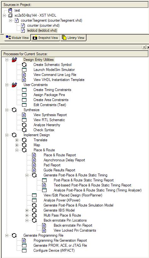
3 5. At this point you should make sure your already compiled and simulated VHDL source code is located in the directory you created in step 3. Next you need to add your source code to the project. In the Sources in Project window, left click on the line where XC2s50 5tq144-XST VHDL (or XC2s50 6tq144-XST) is located to highlight that entry. Using the pull-down menu (or alternatively the right mouse click) select Project > Add Source. Now enter your source code through the Add Existing Sources window by highlighting the desired source code and pressing Open. Note if you are using a hierarchical design, enter the high level module first. You may be asked to clarify what is the source via the Choose Source Type window. Make sure VHDL Module is highlighted and press OK. 6. Xilinx Project Navigator will load your design and the windows will look something similar to what is illustrated below. It should be noted that the example used in this tutorial is a hierarchical design. It has an ARCHITECTURE block with two components (counter & leddcd). The high-level ARCHITECTURE is defined in the file counter7segment.vhd. If using a hierarchical design, the other files must be added. Repeat step 5, but highlight each component to load its associated VHDL file. If you successfully complete this action, there will be check marks to the left of your design name(s) 3

4 7. Now you are ready to synthesize your design to make a netlist. To begin with the options of the Processes for Current Source Window is provided below. 4
5 5
.")
6 To synthesize your design, double left click on Synthesize in the Processes for Current Source: window or right click on Synthesize and select Run or Rerun (the latter instructions will depend on whether or not you have selected to synthesize your design on an earlier occasion). The following will result: 6

7 7. Now you are ready to route, place and map your netlist onto a Spartan II FPGA (which is used on the XESS XSA-50 FPGA protoboard). To route, place and map your design, double left click on Implement Design in the Processes for Current Source: window or right click on Implement Design and select Run or Rerun (the latter instructions will depend on whether or not you have selected to route, place and map your design on an earlier occasion). The following will result: 7

8 8. Before you generate your bit stream to download onto the FPGA, you must first define your I/O to be used on the XESS XSA-50 FPGA protoboard. The pin definitions for various I/O devices used in EE451 can be found in the EE451 website under Tips > XESS Corporation FPGA Protoboard > I/O Pin Mappings. In this particular example, we will define the clock input and outputs to a 7-segment display. First we must attach an implementation or user constraints file (or *.ucf file) to the XC2s50 5tq144-XST VHDL (or XC2s50 6tq144-XST) definition of the FPGA. To do this, highlight the XC2s50 5tq144-XST VHDL (or XC2s50 6tq144-XST) in the Sources in Project: window. Using the pull-down menu (or alternatively the right mouse click) select Project > New Source. A New window will be displayed as illustrated below. Highlight the Implementation Constraints File entry and enter a name of your implementation constraints file. Press Next. 8


9 In a hierarchical design, select you top-level source code filename as illustrated below and press Next. The following screen will be displayed. Simply press Finish. 9

10 In the Sources in Project: window the *.ucf file is now added to your design. Make sure you highlight your top-level design in the Sources in Project: window. In the Processes For Current Sources: window, double click on the following application: User Constraints > Create Timing Constraints. The Xilinx Constraints Editor Window will be displayed. Ensure you have the Ports tab selected. You can enter the I/O to/from your FPGA as being used on the XESS XSA-50 FPGA protoboard. Ensure you enter a P for pin before each pin number. The results are shown below. Make sure you save the mappings to the *.ucf file that you just created for possible future use. In the Xilinx Constraints Editor pull-down menu, select File > Save. If you use this file in the future, you do not need to create it as in step 8. All you do is add the *.ucf file to your design. Additionally, since the route, place and map procedures done in step 7 mapped I/O without a user constraints file, you may have to repeat step 7 with the user constraints file that you just created. 10

11 9. Now you are ready to create the bit stream to be downloaded to the XESS XSA-50 FPGA protoboard. Ensure your design is selected in the Sources in Project: window. In the Processes for Current Source: window, double left click on Generate Programming File or right click on Generate Programming File and select Run or Rerun (the latter instructions will depend on whether or not you have selected to create a bit stream on an earlier occasion). The following will result: 11
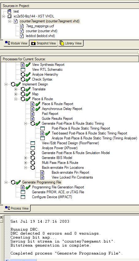
12 12

13 10. Now you are ready to download your bit stream onto the XESS XSA-50 FPGA protoboard. To accomplish this, we must use the XESS GXSLOAD utility. The utility can be found in Start > Engineering Applications > XESS > GXSLOAD or using the following icon: The following application will be started for download. Use the My Computer windows feature to go to the subdirectory where your subdirectory you created in step 3 is located. Simply drag the *.bit file into the FPGA/CPLD of the GXSLOAD utility. Now press Load. The bit stream will be downloaded onto the XESS XSA-50 FPGA protoboard. 11. Now you can demonstrate that your design is properly working. Helpful Tools Associated with Xilinx Project Navigator: In the Processes for Current Source: window there are some utilities and reports that can help you with your design. 1. To observe where your signals were mapped onto the FPGA, your can look at the PAD Report. This can be found at Implement Design > Place & Route > Pad Report 2. Once your constraints file is created, instead of using the Xilinx Constraints Editor, you can simply edit the results. This can be done by executing User Constraints > Edit Constraints (Text) or you can go back to the Xilinx Constraints Editor by executing User Constraints > Create Timing Constraints 13
5 January ModelSim v5.7 Quick Reference Guide
 5 January 2004 ModelSim v5.7 Quick Reference Guide Author: David M. Sendek Background: This guide provides you with step-by-step procedures in using ModelSim to compile, link and simulate your VHDL or
Introduction to WebPACK 6.3. Using Xilinx WebPACK Software to Create FPGA Designs for the XSA Board
 Introduction to WebPACK 6.3 Using Xilinx WebPACK Software to Create FPGA Designs for the XSA Board Release date: 1/1/2005 2005 by XESS Corp. All XS-prefix product designations are trademarks of XESS Corp.
Physics 623. FPGA I Construction of a Synchronous Counter Aug. 4, 2008
 Physics 623 FPGA I onstruction of a Synchronous ounter Aug. 4, 2008 1 The Goal of This Experiment You will design a small digital circuit, download the design to a Field Programmable Gate Array (FPGA)
Tutorial: Working with Verilog and the Xilinx FPGA in ISE 9.2i
 Tutorial: Working with Verilog and the Xilinx FPGA in ISE 9.2i This tutorial will show you how to: Use Verilog to specify a design Simulate that Verilog design Define pin constraints for the FPGA (.ucf
Programming Xilinx SPARTAN 3 Board (Simulation through Implementation)
") Programming Xilinx SPARTAN 3 Board (Simulation through Implementation) September 2008 Prepared by: Oluwayomi Adamo Class: Project IV University of North Texas FPGA Physical Description 4 1. VGA (HD-15)
Programming Xilinx SPARTAN 3 Board (Simulation through Implementation) September 2008 Prepared by: Oluwayomi Adamo Class: Project IV University of North Texas FPGA Physical Description 4 1. VGA (HD-15)
Xilinx ISE8.1 and Spartan-3 Tutorial EE3810
 Xilinx ISE8.1 and Spartan-3 Tutorial EE3810 1 Part1) Starting a new project Simple 3-to-8 Decoder Start the Xilinx ISE 8.1i Project Navigator: Select File > New Project in the opened window 2 Select a
Introduction to WebPACK 8.1. Using Xilinx WebPACK Software to Create FPGA Designs for the XSA Board
 Introduction to WebPACK 8.1 Using Xilinx WebPACK Software to Create FPGA Designs for the XSA Board Release date: 5/16/2005 2006 by XESS Corp. All XS-prefix product designations are trademarks of XESS
Introduction to WebPACK 6.1. Using Xilinx WebPACK Software to Create FPGA Designs for the XSA Board
 Introduction to WebPACK 6.1 Using Xilinx WebPACK Software to Create FPGA Designs for the XSA Board Release date: 10/30/2003 All XS-prefix product designations are trademarks of XESS Corp. All XC-prefix
Introduction to WebPACK 4.1 for FPGAs. Using Xilinx WebPACK Software to Create FPGA Designs for the XSA Board
 Introduction to WebPACK 4.1 for FPGAs Using Xilinx WebPACK Software to Create FPGA Designs for the XSA Board Release date: 10/29/2001 All XS-prefix product designations are trademarks of XESS Corp. All
MANUAL XILINX ISE PROJECT NAVIGATOR
 Hochschule für Angewandte Wissenschaften Hamburg University of Applied Sciences Department of Electrical Engineering and Computer Sciences MANUAL XILINX ISE PROJECT NAVIGATOR AND MODELSIM Design Flow for
EE 1315 DIGITAL LOGIC LAB EE Dept, UMD
 EE 1315 DIGITAL LOGIC LAB EE Dept, UMD EXPERIMENT # 1: Logic building blocks The main objective of this experiment is to let you familiarize with the lab equipment and learn about the operation of the
Using XILINX WebPACK Software to Create CPLD Designs
 Introduction to WebPACK Using XILINX WebPACK Software to Create CPLD Designs RELEASE DATE: 10/24/1999 All XS-prefix product designations are trademarks of XESS Corp. All XC-prefix product designations
Xilinx ISE8.1 and Spartan-3 Tutorial (Prepared by Kahraman Akdemir based on Professor Duckworth's Tutorials updated September 2006)
") Xilinx ISE8.1 and Spartan-3 Tutorial (Prepared by Kahraman Akdemir based on Professor Duckworth's Tutorials updated September 2006) 1 Part1) Starting a new project Simple 3-to-8 Decoder Start the Xilinx
Xilinx ISE8.1 and Spartan-3 Tutorial (Prepared by Kahraman Akdemir based on Professor Duckworth's Tutorials updated September 2006) 1 Part1) Starting a new project Simple 3-to-8 Decoder Start the Xilinx
Chapter 9: Integration of Full ASIP and its FPGA Implementation
 Chapter 9: Integration of Full ASIP and its FPGA Implementation 9.1 Introduction A top-level module has been created for the ASIP in VHDL in which all the blocks have been instantiated at the Register
ECT 224: Digital Computer Fundamentals Using Xilinx StateCAD
 ECT 224: Digital Computer Fundamentals Using Xilinx StateCAD 1) Sequential circuit design often starts with a problem statement tat can be realized in the form of a state diagram or state table a) Xilinx
Introduction to WebPACK 3.1. Using XILINX WebPACK Software to Create CPLD Designs
 Introduction to WebPACK 3.1 Using XILINX WebPACK Software to Create CPLD Designs RELEASE DATE: 8/28/2000 All XS-prefix product designations are trademarks of XESS Corp. All XC-prefix product designations
Getting started with the Xilinx Project Navigator and the Digilent BASYS 2 board.
 Getting started with the Xilinx Project Navigator and the Digilent BASYS 2 board. This lab is based on: Xilinx Project Navigator, Release Version 14.6 Digilent Adept System Rev 2.7, Runtime Rev 2.16 Digilent
Introduction to WebPACK 5.2 for FPGAs. Using Xilinx WebPACK Software to Create FPGA Designs for the XSB-300E Board
 Introduction to WebPACK 5.2 for FPGAs Using Xilinx WebPACK Software to Create FPGA Designs for the XSB-300E Board Release date: 10/27/2003 All XS-prefix product designations are trademarks of XESS Corp.
Logic Implementation on a Xilinx FPGA using VHDL WWU Linux platform assumed. rev 10/25/16
 1 Logic Implementation on a Xilinx FPGA using VHDL WWU Linux platform assumed. rev 10/25/16 The following is a general outline of steps (i.e. design flow) used to implement a digital system described with
Xilinx ISE Synthesis Tutorial
 Xilinx ISE Synthesis Tutorial The following tutorial provides a basic description of how to use Xilinx ISE to create a simple 2-input AND gate and synthesize the design onto the Spartan-3E Starter Board
Using Synplify Pro, ISE and ModelSim
 Using Synplify Pro, ISE and ModelSim VLSI Systems on Chip ET4 351 Rene van Leuken Huib Lincklaen Arriëns Rev. 1.2 The EDA programs that will be used are: For RTL synthesis: Synplicity Synplify Pro For
AccelDSP tutorial 2 (Matlab.m to HDL for Xilinx) Ronak Gandhi Syracuse University Fall
 Ronak Gandhi Syracuse University Fall") AccelDSP tutorial 2 (Matlab.m to HDL for Xilinx) Ronak Gandhi Syracuse University Fall 2009-10 AccelDSP Getting Started Tutorial Introduction This tutorial exercise will guide you through the process of
AccelDSP tutorial 2 (Matlab.m to HDL for Xilinx) Ronak Gandhi Syracuse University Fall 2009-10 AccelDSP Getting Started Tutorial Introduction This tutorial exercise will guide you through the process of
Physics 623. Programmable Gate Array Experiment Nov. 30, 2006
 Physics 623 Programmable Gate Array Experiment Nov. 30, 2006 1 The Goal of This Experiment You will design a small digital circuit, download the design to a Field Programmable Gate Array (FPGA) I, and
Xilinx Tutorial Basic Walk-through
 Introduction to Digital Logic Design with FPGA s: Digital logic circuits form the basis of all digital electronic devices. FPGAs (Field Programmable Gate Array) are large programmable digital electronic
Verilog Design Entry, Synthesis, and Behavioral Simulation
 ------------------------------------------------------------- PURPOSE - This lab will present a brief overview of a typical design flow and then will start to walk you through some typical tasks and familiarize
CPLD Experiment 4. XOR and XNOR Gates with Applications
 CPLD Experiment 4 XOR and XNOR Gates with Applications Based on Xilinx ISE Design Suit 10.1 Department of Electrical & Computer Engineering Florida International University Objectives Materials Examining
Logic Implementation on a Xilinx FPGA using VHDL WWU Linux platform assumed. rev 11/01/17
 1 Logic Implementation on a Xilinx FPGA using VHDL WWU Linux platform assumed. rev 11/01/17 The following is a general outline of steps (i.e. design flow) used to implement a digital system described with
Implementing a Verilog design into the UWEE CPLD Development Board Using Xilinx s ISE 7.1i Software: A Tutorial
 Implementing a Verilog design into the UWEE CPLD Development Board Using Xilinx s ISE 7.1i Software: A Tutorial Revision 0 By: Evan Gander Materials: The following are required in order to complete this
and 32 bit for 32 bit. If you don t pay attention to this, there will be unexpected behavior in the ISE software and thing may not work properly!
 This tutorial will show you how to: Part I: Set up a new project in ISE 14.7 Part II: Implement a function using Schematics Part III: Simulate the schematic circuit using ISim Part IV: Constraint, Synthesize,
Tutorial on FPGA Design Flow based on Xilinx ISE WebPack and ModelSim. ver. 2.0
 Tutorial on FPGA Design Flow based on Xilinx ISE WebPack and ModelSim ver. 2.0 Updated: Fall 2013 1 Preparing the Input: Download examples associated with this tutorial posted at http://ece.gmu.edu/tutorials-and-lab-manuals
University of Hawaii EE 361L. Getting Started with Spartan 3E Digilent Basys2 Board. Lab 4.1
 University of Hawaii EE 361L Getting Started with Spartan 3E Digilent Basys2 Board Lab 4.1 I. Test Basys2 Board Attach the Basys2 board to the PC or laptop with the USB connector. Make sure the blue jumper
Introduction to WebPACK 4.1 for CPLDs. Using Xilinx WebPACK Software to Create CPLD Designs for the XS95 Board
 Introduction to WebPACK 4.1 for CPLDs Using Xilinx WebPACK Software to Create CPLD Designs for the XS95 Board Release date: 10/29/2001 All XS-prefix product designations are trademarks of XESS Corp. All
Tutorial on FPGA Design Flow based on Aldec Active HDL. Ver 1.5
 Tutorial on FPGA Design Flow based on Aldec Active HDL Ver 1.5 1 Prepared by Ekawat (Ice) Homsirikamol, Marcin Rogawski, Jeremy Kelly, John Pham, and Dr. Kris Gaj This tutorial assumes that you have basic
Revision: February 27, E Main Suite D Pullman, WA (509) Voice and Fax
 Voice and Fax") Xilinx ISE WebPACK Schematic Capture Tutorial Revision: February 27, 2010 215 E Main Suite D Pullman, WA 99163 (509) 334 6306 Voice and Fax Overview This tutorial provides instruction for using the Xilinx
Xilinx ISE WebPACK Schematic Capture Tutorial Revision: February 27, 2010 215 E Main Suite D Pullman, WA 99163 (509) 334 6306 Voice and Fax Overview This tutorial provides instruction for using the Xilinx
Digital Circuit Design Using Xilinx ISE Tools
 Digital Circuit Design Using Xilinx ISE Tools Poras T. Balsara and Prashant Vallur Table of Contents 1. Introduction 2. Programmable logic devices: FPGA and CPLD 3. Creating a new project in Xilinx Foundation
ECE 4305 Computer Architecture Lab #1
 ECE 4305 Computer Architecture Lab #1 The objective of this lab is for students to familiarize with the FPGA prototyping system board (Nexys-2) and the Xilinx software development environment that will
Nexys 2/3 board tutorial (Decoder, ISE 13.2) Jim Duckworth, August 2011, WPI. (updated March 2012 to include Nexys2 board)
 Jim Duckworth, August 2011, WPI. (updated March 2012 to include Nexys2 board)") Nexys 2/3 board tutorial (Decoder, ISE 13.2) Jim Duckworth, August 2011, WPI. (updated March 2012 to include Nexys2 board) Note: you will need the Xilinx ISE Webpack installed on your computer (or you
Nexys 2/3 board tutorial (Decoder, ISE 13.2) Jim Duckworth, August 2011, WPI. (updated March 2012 to include Nexys2 board) Note: you will need the Xilinx ISE Webpack installed on your computer (or you
Altera Quartus II Tutorial ECE 552
 Altera Quartus II Tutorial ECE 552 Quartus II by Altera is a PLD Design Software which is suitable for high-density Field-Programmable Gate Array (FPGA) designs, low-cost FPGA designs, and Complex Programmable
Contents. Appendix B HDL Entry Tutorial 2 Page 1 of 14
 Appendix B HDL Entry Tutorial 2 Page 1 of 14 Contents Appendix B HDL Entry Tutorial 2...2 B.1 Getting Started...2 B.1.1 Preparing a Folder for the Project...2 B.1.2 Starting Quartus II...2 B.1.3 Creating
FPGA Design Flow 1. All About FPGA
 FPGA Design Flow 1 In this part of tutorial we are going to have a short intro on FPGA design flow. A simplified version of FPGA design flow is given in the flowing diagram. FPGA Design Flow 2 FPGA_Design_FLOW
Banks, Jasmine Elizabeth (2011) The Spartan 3E Tutorial 1 : Introduction to FPGA Programming, Version 1.0. [Tutorial Programme]
![Banks, Jasmine Elizabeth (2011) The Spartan 3E Tutorial 1 : Introduction to FPGA Programming, Version 1.0. [Tutorial Programme]](/thumbs/75/72381729.jpg "Banks, Jasmine Elizabeth (2011) The Spartan 3E Tutorial 1 : Introduction to FPGA Programming, Version 1.0. [Tutorial Programme]") QUT Digital Repository: http://eprints.qut.edu.au/ This is the author version published as: This is the accepted version of this article. To be published as : This is the author s version published as:
QUT Digital Repository: http://eprints.qut.edu.au/ This is the author version published as: This is the accepted version of this article. To be published as : This is the author s version published as:
Board-Data Processing. VHDL Exercises. Exercise 1: Basics of VHDL Programming. Stages of the Development process using FPGA s in Xilinx ISE.
 Board-Data Processing VHDL Exercises Exercise 1: Basics of VHDL Programming Stages of the Development process using FPGA s in Xilinx ISE. Basics of VHDL VHDL (Very High Speed IC Hardware description Language)
Tutorial on FPGA Design Flow based on Xilinx ISE Webpack andisim. ver. 1.0
 Tutorial on FPGA Design Flow based on Xilinx ISE Webpack andisim ver. 1.0 1 Prepared by Malik Umar Sharif and Dr. Kris Gaj The example codes used in this tutorial can be obtained from http://ece.gmu.edu/coursewebpages/ece/ece448/s11/labs/448_lab3.htm
EE 367 Logic Design Lab #1 Introduction to Xilinx ISE and the ML40X Eval Board Date: 1/21/09 Due: 1/28/09
 EE 367 Logic Design Lab #1 Introduction to Xilinx ISE and the ML40X Eval Board Date: 1/21/09 Due: 1/28/09 Lab Description Today s lab will introduce you to the Xilinx Integrated Software Environment (ISE)
PlanAhead Software Tutorial
 PlanAhead Software Tutorial RTL Design and IP Generation The information disclosed to you hereunder (the Information ) is provided AS-IS with no warranty of any kind, express or implied. Xilinx does not
Tutorial - Using Xilinx System Generator 14.6 for Co-Simulation on Digilent NEXYS3 (Spartan-6) Board
 Board") Tutorial - Using Xilinx System Generator 14.6 for Co-Simulation on Digilent NEXYS3 (Spartan-6) Board Shawki Areibi August 15, 2017 1 Introduction Xilinx System Generator provides a set of Simulink blocks
Tutorial - Using Xilinx System Generator 14.6 for Co-Simulation on Digilent NEXYS3 (Spartan-6) Board Shawki Areibi August 15, 2017 1 Introduction Xilinx System Generator provides a set of Simulink blocks
TLL5000 Electronic System Design Base Module. Getting Started Guide, Ver 3.4
 TLL5000 Electronic System Design Base Module Getting Started Guide, Ver 3.4 COPYRIGHT NOTICE The Learning Labs, Inc. ( TLL ) All rights reserved, 2008 Reproduction in any form without permission is prohibited.
ECE 491 Laboratory 1 Introducing FPGA Design with Verilog September 6, 2004
 Goals ECE 491 Laboratory 1 Introducing FPGA Design with Verilog September 6, 2004 1. To review the use of Verilog for combinational logic design. 2. To become familiar with using the Xilinx ISE software
Tutorial on FPGA Design Flow based on Aldec Active HDL. Ver 1.5
 Tutorial on FPGA Design Flow based on Aldec Active HDL Ver 1.5 1 Prepared by Ekawat (Ice) Homsirikamol, Marcin Rogawski, Jeremy Kelly, Kishore Kumar Surapathi and Dr. Kris Gaj This tutorial assumes that
Lab 6: Intro to FPGAs
 Lab 6: Intro to FPGAs UC Davis Physics 116B Rev 2/22/2018 There s a saying when dealing with complex electronic systems: If you can make the LED blink, you re 90% of the way there., so in this lab you
Tutorial on FPGA Design Flow based on Xilinx ISE Webpack and ModelSim. ver. 1.5
 Tutorial on FPGA Design Flow based on Xilinx ISE Webpack and ModelSim ver. 1.5 1 Prepared by Marcin Rogawski, Ekawat (Ice) Homsirikamol, Kishore Kumar Surapathi and Dr. Kris Gaj The example codes used
Lab 1: Introduction to Verilog HDL and the Xilinx ISE
 EE 231-1 - Fall 2016 Lab 1: Introduction to Verilog HDL and the Xilinx ISE Introduction In this lab simple circuits will be designed by programming the field-programmable gate array (FPGA). At the end
TLL5000 Electronic System Design Base Module
 TLL5000 Electronic System Design Base Module The Learning Labs, Inc. Copyright 2007 Manual Revision 2007.12.28 1 Copyright 2007 The Learning Labs, Inc. Copyright Notice The Learning Labs, Inc. ( TLL )
Xilinx Schematic Entry Tutorial
 Overview Xilinx Schematic Entry Tutorial Xilinx ISE Schematic Entry & Modelsim Simulation What is circuit simulation and why is it important? Complex designs, short design cycle Simultaneous system design
2001 by X Engineering Software Systems Corp., Apex, North Carolina 27502
 2001 by X Engineering Software Systems Corp., Apex, North Carolina 27502 All rights reserved. No part of this text may be reproduced, in any form or by any means, without permission in writing from the
Revision: February 27, E Main Suite D Pullman, WA (509) Voice and Fax
 Voice and Fax") Xilinx ISE WebPACK VHDL Tutorial Revision: February 27, 2010 215 E Main Suite D Pullman, WA 99163 (509) 334 6306 Voice and Fax Overview This tutorial provides simple instruction for using the Xilinx ISE
Xilinx ISE WebPACK VHDL Tutorial Revision: February 27, 2010 215 E Main Suite D Pullman, WA 99163 (509) 334 6306 Voice and Fax Overview This tutorial provides simple instruction for using the Xilinx ISE
Tutorial on FPGA Design Flow based on Xilinx ISE Webpack and ModelSim. ver. 1.3
 Tutorial on FPGA Design Flow based on Xilinx ISE Webpack and ModelSim ver. 1.3 1 Prepared by Marcin Rogawski, Ekawat (Ice) Homsirikamol, Kishorekum Surapathi, and Dr. Kris Gaj The example codes used in
Quick Front-to-Back Overview Tutorial
 Quick Front-to-Back Overview Tutorial PlanAhead Design Tool This tutorial document was last validated using the following software version: ISE Design Suite 14.5 If using a later software version, there
EE183 LAB TUTORIAL. Introduction. Projects. Design Entry
 EE183 LAB TUTORIAL Introduction You will be using several CAD tools to implement your designs in EE183. The purpose of this lab tutorial is to introduce you to the tools that you will be using, Xilinx
ISE Design Suite Software Manuals and Help
 ISE Design Suite Software Manuals and Help These documents support the Xilinx ISE Design Suite. Click a document title on the left to view a document, or click a design step in the following figure to
Circuit design with configurable devices (FPGA)
") 1 Material Circuit design with configurable devices (FPGA) Computer with Xilinx's ISE software installed. Digilent's Basys2 prototype board and documentation. Sample design files (lab kit). Files and documents
1 Material Circuit design with configurable devices (FPGA) Computer with Xilinx's ISE software installed. Digilent's Basys2 prototype board and documentation. Sample design files (lab kit). Files and documents
Building Combinatorial Circuit Using Behavioral Modeling Lab
 Building Combinatorial Circuit Using Behavioral Modeling Lab Overview: In this lab you will learn how to model a combinatorial circuit using behavioral modeling style of Verilog HDL. You will model a combinatorial
PlanAhead Release Notes
 PlanAhead Release Notes What s New in the 11.1 Release UG656(v 11.1.0) April 27, 2009 PlanAhead 11.1 Release Notes Page 1 Table of Contents What s New in the PlanAhead 11.1 Release... 4 Device Support...
EMT1250 LABORATORY EXPERIMENT. EXPERIMENT # 6: Quartus II Tutorial and Practice. Name: Date:
 EXPERIMENT # 6: Quartus II Tutorial and Practice Name: Date: Equipment/Parts Needed: Quartus II R Web Edition V9.1 SP2 software by Altera Corporation USB drive to save your files Objective: Learn how to
The board is powered by the USB connection, so to turn it on or off you plug it in or unplug it, respectively.
 Lab 1 You may work in pairs or individually on this lab Lab Objectives Learn about the equipment we will be using and how to handle it safely. Learn the basics of using Xilinx ISE to develop hardware designs
RTL and Technology Schematic Viewers Tutorial. UG685 (v13.1) March 1, 2011
 March 1, 2011") RTL and Technology Schematic Viewers Tutorial The information disclosed to you hereunder (the Information ) is provided AS-IS with no warranty of any kind, express or implied. Xilinx does not assume any
RTL and Technology Schematic Viewers Tutorial The information disclosed to you hereunder (the Information ) is provided AS-IS with no warranty of any kind, express or implied. Xilinx does not assume any
Tutorial: ISE 12.2 and the Spartan3e Board v August 2010
 Tutorial: ISE 12.2 and the Spartan3e Board v12.2.1 August 2010 This tutorial will show you how to: Use a combination of schematics and Verilog to specify a design Simulate that design Define pin constraints
RTL Design and IP Generation Tutorial. PlanAhead Design Tool
 RTL Design and IP Generation Tutorial PlanAhead Design Tool Notice of Disclaimer The information disclosed to you hereunder (the "Materials") is provided solely for the selection and use of Xilinx products.
XILINX WebPack -- testing with Nexys2 boards at USC (EE201L)
") XILINX WebPack -- testing with Nexys2 boards at USC (EE201L) Gandhi Puvvada 1 Before you start: 1.1 We assume that you have installed WebPACK on your desktop or laptop already. We assume that you have
XILINX WebPack -- testing with Nexys2 boards at USC (EE201L) Gandhi Puvvada 1 Before you start: 1.1 We assume that you have installed WebPACK on your desktop or laptop already. We assume that you have
Getting Started with Xilinx Design Tools and the XS 40 Prototyping Platform-- a User s Guide *
 Getting Started with Xilinx Design Tools and the XS 40 Prototyping Platform-- a User s Guide * B. Earl Wells Sin Ming Loo by Electrical and Computer Engineering Department University of Alabama in Huntsville
Laboratory #Intro to Xilinx ISE and CR-2 Kit ECE 332
 Name: G Number: 1 Introduction Laboratory #Intro to Xilinx ISE and CR-2 Kit ECE 332 The purpose of this laboratory is to introduce the design tools used in ECE 332 lab. In this lab you will learn about
FPGA Design Tutorial
 ECE 554 Digital Engineering Laboratory FPGA Design Tutorial Version 5.0 Fall 2006 Updated Tutorial: Jake Adriaens Original Tutorial: Matt King, Surin Kittitornkun and Charles R. Kime Table of Contents
ENGN 1630: CPLD Simulation Fall ENGN 1630 Fall Simulating XC9572XLs on the ENGN1630 CPLD-II Board Using Xilinx ISim
 ENGN 1630 Fall 2018 Simulating XC9572XLs on the ENGN1630 CPLD-II Board Using Xilinx ISim You will use the Xilinx ISim simulation software for the required timing simulation of the XC9572XL CPLD programmable
VIVADO TUTORIAL- TIMING AND POWER ANALYSIS
 VIVADO TUTORIAL- TIMING AND POWER ANALYSIS IMPORTING THE PROJECT FROM ISE TO VIVADO Initially for migrating the same project which we did in ISE 14.7 to Vivado 2016.1 you will need to follow the steps
Implementation of a Fail-Safe Design in the Spartan-6 Family Using ISE Design Suite XAPP1104 (v1.0.1) June 19, 2013
 June 19, 2013") Implementation of a Fail-Safe Design in the Spartan-6 Family Using ISE Design Suite 12.4 Notice of Disclaimer The information disclosed to you hereunder (the Materials ) is provided solely for the selection
Implementation of a Fail-Safe Design in the Spartan-6 Family Using ISE Design Suite 12.4 Notice of Disclaimer The information disclosed to you hereunder (the Materials ) is provided solely for the selection
Tutorial for Altera DE1 and Quartus II
 Tutorial for Altera DE1 and Quartus II Qin-Zhong Ye December, 2013 This tutorial teaches you the basic steps to use Quartus II version 13.0 to program Altera s FPGA, Cyclone II EP2C20 on the Development
Getting Started with Xilinx WebPack 13.1
 Getting Started with Xilinx WebPack 13.1 B. Ackland June 2011 (Adapted from S. Tewksbury notes WebPack 7.1) This tutorial is designed to help you to become familiar with the operation of the WebPack software
Tutorial on FPGA Design Flow based on Aldec Active HDL. ver 1.6
 Tutorial on FPGA Design Flow based on Aldec Active HDL ver 1.6 Fall 2011 1 Prepared by Ekawat (Ice) Homsirikamol, Marcin Rogawski, Jeremy Kelly, Kishore Kumar Surapathi, Ambarish Vyas, Umar Sharif and
Xilinx ChipScope ICON/VIO/ILA Tutorial
 Xilinx ChipScope ICON/VIO/ILA Tutorial The Xilinx ChipScope tools package has several modules that you can add to your Verilog design to capture input and output directly from the FPGA hardware. These
Introduction. About this tutorial. How to use this tutorial
 Basic Entry & not About this tutorial This tutorial consists of an introduction to creating simple circuits on an FPGA using a variety of methods. There are two ways to create the circuit: using or by
Tutorial on FPGA Design Flow based on Aldec Active HDL. ver 1.7
 Tutorial on FPGA Design Flow based on Aldec Active HDL ver 1.7 Fall 2012 1 Prepared by Ekawat (Ice) Homsirikamol, Marcin Rogawski, Jeremy Kelly, Kishore Kumar Surapathi, Ambarish Vyas, Malik Umar Sharif
Circuit Design and Simulation with VHDL 2nd edition Volnei A. Pedroni MIT Press, 2010 Book web:
 Circuit Design and Simulation with VHDL 2nd edition Volnei A. Pedroni MIT Press, 2010 Book web: www.vhdl.us Appendix C Xilinx ISE Tutorial (ISE 11.1) This tutorial is based on ISE 11.1 WebPack (free at
Vivado Design Suite Tutorial. Designing IP Subsystems Using IP Integrator
 Vivado Design Suite Tutorial Designing IP Subsystems Using IP Integrator Notice of Disclaimer The information disclosed to you hereunder (the "Materials") is provided solely for the selection and use of
Engineering 1630 Fall Simulating XC9572XL s on the ENGN1630 CPLD-II Board
 Engineering 1630 Fall 2016 Simulating XC9572XL s on the ENGN1630 CPLD-II Board You will use the Aldec Active-HDL software for the required timing simulation of the XC9572XL CPLD programmable logic chips
CSE 591: Advanced Hardware Design and Verification (2012 Spring) LAB #0
 LAB #0") Lab 0: Tutorial on Xilinx Project Navigator & ALDEC s Active-HDL Simulator CSE 591: Advanced Hardware Design and Verification Assigned: 01/05/2011 Due: 01/19/2011 Table of Contents 1 Overview... 2 1.1
Lab 0: Tutorial on Xilinx Project Navigator & ALDEC s Active-HDL Simulator CSE 591: Advanced Hardware Design and Verification Assigned: 01/05/2011 Due: 01/19/2011 Table of Contents 1 Overview... 2 1.1
FPGA Interfacing of HD44780 Based LCD Using Delayed Finite State Machine (FSM)
") FPGA Interfacing of HD44780 Based LCD Using Delayed Finite State Machine (FSM) Edwin NC Mui Custom R & D Engineer Texco Enterprise Ptd. Ltd. {blackgrail2000@hotmail.com} Abstract This paper presents a
FPGA Interfacing of HD44780 Based LCD Using Delayed Finite State Machine (FSM) Edwin NC Mui Custom R & D Engineer Texco Enterprise Ptd. Ltd. {blackgrail2000@hotmail.com} Abstract This paper presents a
ELEC 204 Digital System Design LABORATORY MANUAL
 ELEC 204 Digital System Design LABORATORY MANUAL : Introductory Tutorial For Xilinx ISE Foundation v10.1 & Implementing XOR Gate College of Engineering Koç University Important Note: In order to effectively
Tutorial: Working with the Xilinx tools 14.4
 Tutorial: Working with the Xilinx tools 14.4 This tutorial will show you how to: Part I: Set up a new project in ISE Part II: Implement a function using Schematics Part III: Implement a function using
Lab 2: Introduction to Verilog HDL and Quartus
 Lab 2: Introduction to Verilog HDL and Quartus September 16, 2008 In the previous lab you designed simple circuits using discrete chips. In this lab you will do the same but by programming the CPLD. At
XILINX ISE AND SPARTAN 3AN TUTORIAL
 XILINX ISE AND SPARTAN 3AN TUTORIAL SYNTETIZE AND SIMULATION------------------------------------------ This tutorial will show you how to create a simple Xilinx ISE project based on the Spartan-3 Board.
Nexys 2 board tutorial (Decoder, ISE 12.2) Jim Duckworth, August 2010, WPI. Digilent Adept Programming Steps added by Zoe (Zhu Fu)
 Jim Duckworth, August 2010, WPI. Digilent Adept Programming Steps added by Zoe (Zhu Fu)") Nexys 2 board tutorial (Decoder, ISE 12.2) Jim Duckworth, August 2010, WPI. Digilent Adept Programming Steps added by Zoe (Zhu Fu) Note: you will need the Xlinx ISE Webpack installed on your compuer (or
Nexys 2 board tutorial (Decoder, ISE 12.2) Jim Duckworth, August 2010, WPI. Digilent Adept Programming Steps added by Zoe (Zhu Fu) Note: you will need the Xlinx ISE Webpack installed on your compuer (or
475 Electronics for physicists Introduction to FPGA programming
 475 Electronics for physicists Introduction to FPGA programming Andrej Seljak, Gary Varner Department of Physics University of Hawaii at Manoa November 18, 2015 Abstract Digital circuits based on binary
PlanAhead Software Tutorial
 PlanAhead Software Tutorial Team Design NOTICE OF DISCLAIMER: The information disclosed to you hereunder (the Information ) is provided AS-IS with no warranty of any kind, express or implied. Xilinx does
ECE 436 Laboratory 4 TARGETING THE XESS PROTO-BOARD AND PHYSICAL TESTING WITH A LOGIC ANALYZER
 ECE 436 Laboratory 4 TARGETING THE XESS PROTO-BOARD AND PHYSICAL TESTING WITH A LOGIC ANALYZER Description: For this laboratory, you will be learning how to constrain your design to FPGA pins, generate
DESIGN STRATEGIES & TOOLS UTILIZED
 CHAPTER 7 DESIGN STRATEGIES & TOOLS UTILIZED 7-1. Field Programmable Gate Array The internal architecture of an FPGA consist of several uncommitted logic blocks in which the design is to be encoded. The
Timing Analysis in Xilinx ISE
 Timing Analysis in Xilinx ISE For each design which is to be implemented, constraints should be defined to get predictable results. The first important class of constraints was already introduced in the
Introduction. In this exercise you will:
 Introduction In a lot of digital designs (DAQ, Trigger,..) the FPGAs are used. The aim of this exercise is to show you a way to logic design in a FPGA. You will learn all the steps from the idea to the
Verilog Simulation Mapping
 1 Motivation UNIVERSITY OF CALIFORNIA AT BERKELEY COLLEGE OF ENGINEERING DEPARTMENT OF ELECTRICAL ENGINEERING AND COMPUTER SCIENCE Lab 4 Verilog Simulation Mapping In this lab you will learn how to use
PINE TRAINING ACADEMY
 PINE TRAINING ACADEMY Course Module A d d r e s s D - 5 5 7, G o v i n d p u r a m, G h a z i a b a d, U. P., 2 0 1 0 1 3, I n d i a Digital Logic System Design using Gates/Verilog or VHDL and Implementation
ECSE-323 Digital System Design. Lab #1 Using the Altera Quartus II Software Fall 2008
 1 ECSE-323 Digital System Design Lab #1 Using the Altera Quartus II Software Fall 2008 2 Introduction. In this lab you will learn the basics of the Altera Quartus II FPGA design software through following