MIC2569. Features. General Description. Applications. Typical Application. CableCARD Power Switch
|
|
|
- Clifford Stanley
- 6 years ago
- Views:
Transcription
1 CableCARD Power Swich General Descripion is designed o supply power o OpenCable sysems and CableCARD hoss. These CableCARDs are also known as Poin of Disribuion (POD) cards. suppors boh Single and Muliple sream cards hrough a simple o conrol parallel inerface. All volage swiching is sof-sar a urn-on, and break-before-make when changing beween differen volage supplies. Buil in curren limiing proecs all V CC and V PP oupu lines of he hos sysem from card fauls and accidenal shor circuis. provides a FAULT/ signal o indicae an over-curren or faul condiion exiss and is equipped wih inernal hermal monioring circuiry o proec he device iself in he even of a susained over-curren condiion. is offered in a space saving 16 pin QSOP packaging. Daa shees and suppor documenaion can be found on Micrel s web sie a Feaures 110 mω maximum V CC on resisance 400 mω maximum V PP on resisance 3.0V o 3.6V for he 3.3V IN operaing range 3.0V o 5.5V for he 5V IN operaing range 1.3A minimum V CC curren limi 150mA minimum V PP curren limi (150mA each) Compac 16-pin QSOP packaging Operaing emperaures from 40 C o +85 C Low quiescen curren Sof sar urn-on Break-before-make volage swiching Shor-circui proecion wih hermal shudown Inpu under volage lock-ou (UVLO) ESD proecion No exernal componens required Applicaions Saellie / Cable / DVR / Television se op boxes Video recorders Game consoles Typical Applicaion OpenCable Power Swich CableCARD is a rademark of CableLabs, Inc. OpenCable is a rademark of Cable Television Laboraories, Inc. Micrel Inc Forune Drive San Jose, CA USA el +1 fax + 1 (408) hp:// Sepember 2007 M C
2 Ordering Informaion Par Number Marking Pb-Free Juncion Temp. Range (1) Package YQS YQS Yes 40 C o +85 C 16-pin QSOP Pin Configuraion 16-Pin QSOP (QS) Sepember M C
3 Pin Descripion Pin Number Pin Name Pin Funcion 1 GND Ground. 2 NIC No inernal connecion. A volage or signal applied o his pin will have no effec on device operaion VIN 3V Supply inpu. Inernal chip power is drawn from his supply. 4 5VIN 5V Supply inpu VIN 6 NIC 7 C1 8 C2 9 C0 10 FAULT/ 11 NIC 3V Supply inpu. Noe: boh 3.3VIN inpus mus be powered o insure raed curren and R ON is me. No inernal connecion. A volage or signal applied o his pin will have no effec on device operaion. Conrol Pins Oupus C2 C1 C0 VCC VPP1 VPP V 3.3 V 3.3 V V 5.0 V 5.0 V Hi-Z Hi-Z Hi-Z Hi-Z GND Hi-Z V GND 5.0 V V 5V GND V GND GND GND GND GND FAULT/ indicaes he occurrence of a faul. FAULT/ is an open drain LOW rue oupu and goes low when any supply oupu is in curren limi or if a hermal faul occurs. No inernal connecion. A volage or signal applied o his pin will have no effec on device operaion. 12 VPP2 VPP2 oupu o CableCARD card VCC 15 NIC VCC (3V main supply) oupu o CableCARD card. Boh oupu pins should be conneced ogeher. No inernal connecion. A volage or signal applied o his pin will have no effec on device operaion. 16 VPP1 VPP1 oupu o CableCARD card. Sepember M C
4 Absolue Maximum Raings (1) Power Supply Volage 5VIN V o +6.0V 3.3VIN V o +3.8V Volage on any oher pin v o +6.0V Coninuous Oupu Curren: VCC... Inernally limied VPP...Inernally limied Curren Ino/Ou of any conrol pin:... ±10mA Juncion Temperaure C Sorage Temperaure C o +150 C Operaing Raings (2) Power Supply Volage 5VIN V o 5.5V 3.3VIN V o 3.6V Coninuous Oupu Curren VCC A VPP ma Ambien Temperaure (T A ) C o +85 C Juncion Temperaure (T J ) C o +125 C Thermal Resisance (θ JA ) C/W Soldering: QSOP Packages Infrared (10 o 20 seconds) C Peak (3) Elecrical Characerisics (4) 3.3V IN = 3.3V; 5V IN = 5.0V; T A = 25 C. Bold values indicae 40 C T A +85 C. Symbol Parameer Condiion Min Typ Max Unis 3.3VIN Operaing inpu volage V 5VIN Operaing inpu volage V I VIN UVLO I 3.3VIN Supply Inpu Curren I 5VIN Supply Inpu Curren Under Volage Lock Ou No Load C2,C1,C0 = No Load C2,C1,C0 = S-Mode M-Mode S-Mode M-Mode µa µa µa µa µa µa µa µa µa µa 3.3VIN rising V 3.3VIN falling V UVLO HYS Hyseresis 80 mv Power Swiches R ON_VCC VCC Swich Resisance: R DS_ON R ON_VPP1 I OUT = 1000 ma mω I OUT = 125 ma V OUT = 3.3 V mω VPP1 Swich Resisance: I OUT = 125 ma V OUT = 5.0 V mω I LIMIT I LIMIT_VCC Oupu Curren Limi: VCC I LIMIT_VPP1 Oupu Curren Limi: VPP 1 VCC = 3.3 V A VPP1 = 3.3 V and VPP1 = 5.0 V ma Sepember M C
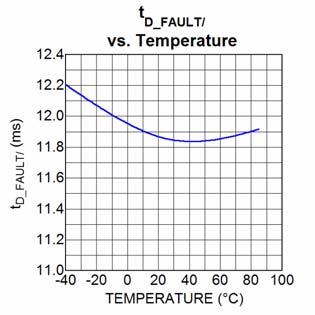
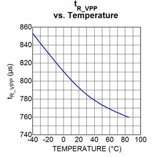
5 I/O Logic Symbol Parameer Condiion Min Typ Max Unis V IL LOW-Level Inpu Volage 1 V V IH HIGH-Level Inpu Volage 2 V Inpu Hyseresis 100 mv I IN_LGC Inpu leakage Curren C2, C1, C µa I OFF Oupu OFF leakage curren FAULT/, V FAULT/ = 5V 4 10 µa V OL_OD Open Drain Oupu LOW Volage FAULT/, I SINK = 1 ma 0.2 V AC Characerisics The S-Mode and M-Mode AC Characerisics are no esed in producion, specified by design. Symbol Parameer Condiion Min Typ Max Unis D_FAULT/ Delay before assering or deassering FAULT/ Faul on VCC, VPP1, or VPP ms S-Mode PWRUP_S-MODE_VCC No Power o VIN Compliance 750 µs Power-up Rise Time Noes 5 & µs PWRUP_S-MODE_VPP ON_ _VPP Oupu Turn On Delay Time 000 o µs Oupu Rise Time Noes 8 & µs R_ _VPP OFF_ _VPP Oupu Turn-Off Delay 001 o µs Oupu Fall Time Noes 8 & µs F_ _VPP OFF_ _VPP Oupu Discharge Delay 001 o µs Oupu Discharge Time Noes 8 & µs F_ _VPP ON_ _VPP Oupu Turn On Delay Time 110 o µs Oupu Rise Time Noes 8 & µs R_ _VPP M-Mode Symbol Parameer Condiion Min Typ Max Unis ON_ _VCC Oupu Turn On Delay Time 50 µs Noes 5 & 6 R_ _VCC Oupu Rise Time 750 µs 011 o 100 ON_ _VPP Oupu Turn On Delay Time 800 µs Noes 8 & 9 Oupu Rise Time 800 µs R_ _VPP OFF_ _VCC Oupu Turn-Off Delay 35 µs Noes 5 & 7 F_ _VCC Oupu Fall Time 25 µs 100 o 010 OFF_ _VPP Oupu Turn-Off Delay 35 µs Noes 8 & 10 Oupu Fall Time 25 µs F_ _VPP Sepember M C
6 Symbol Parameer Condiion Min Typ Max Unis OFF_ _VCC Oupu Discharge Delay 35 µs Noes 5 & 7 F_ _VCC Oupu Discharge Time 25 µs 100 o 111 OFF_ _VPP Oupu Discharge Delay 35 µs Noes 8 & 10 Oupu Discharge Time 25 µs F_ _VPP Noes: 1. Exceeding he absolue maximum raing may damage he device. 2. The device is no guaraneed o funcion ouside is operaing raing. 3. Devices are ESD sensiive. Handling precauions recommended. Human body model, 1.5k in series wih 100pF. 4. Specificaion for packaged produc only. 5. RL = 10Ω, CL = 1µF, See Figures 1, Maximum ransiion ime o 3.3 V compliance, from any sae including VCC equal o GND. 7. Maximum ransiion ime o GND, from any sae including VCC equal o 3.6 V. 8. RL = 100Ω, CL = 0.1µF, See Figures 1, 2 9. Maximum ransiion ime o 5 V compliance, from any sae including VPP equal o GND. 10. Maximum ransiion ime o GND, from any sae including VPP equal o 5.5 V. Sepember M C
7 Timing Diagram Figure 1. Turn-On and Turn-Off Delay Figure 2. Rise and Fall Time Sepember M C


8 Typical Characerisics Sepember M C


9 Sepember M C

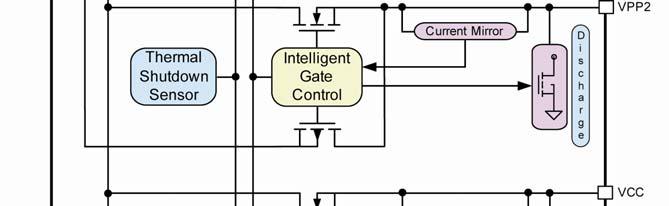
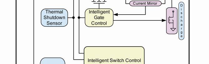

10 Funcional Characerisics Block Diagram Sepember M C
11 Funcional Descripion 3.3VIN and 5.0VIN 3.3VIN and 5VIN are he inpu power supplies for he. 3.3VIN powers he s inernal funcions; as well as, VCC, and VPP1 and VPP2. 5VIN provides power o VPP1 and VPP2. Tables 1 and 2 shows he conrol saes which supply is provided o which oupu C0, C1, C2 (Saes Conrols) C0, C1, and C2 conrol he oupu condiions for VCC, VPP1 and VPP2. C0, C1, and C2 are inpus o he provided by he hos. See Tables 1 and 2 for a complee lising. Also see he Applicaion Informaion secion. VCC VCC provides he main 3.3V supply o he CableCARD device. VCC is proeced agains high curren condiions and shor circuis. The minimum curren limi is se o 1.3A from 3.3VIN. Breakbefore-make swiching prevens crossed connecions during sae changes. The VCC oupu depends on he hos / card combinaion. See Tables 1 and 2 for a complee lising. Also see he Applicaion Informaion secion. VPP1, VPP2 (VPP1/2) VPP1 and VPP2 provide he 3.3V and 5.0V supplies o he CableCARD device. VPP1 and VPP2 are proeced agains high curren condiions and shor circuis. The minimum curren limi is se o a minimum of 150mA. Noe: VPP1 and VPP2 are powered separaely wih each having a curren limi of 150mA Break-before-make swiching prevens crossed connecions during sae changes. The VPP1/2 oupu depends on he hos / card combinaion. See Tables 1 and 2 for a complee lising. Also see he Applicaion Informaion secion. Sof-Sar The VCC, VPP1 and VPP2 oupus are all slew rae conrolled insuring a sof-sar urn-on characerisic. Sof-saring is in effec anyime a supply ramps from a 0V condiion or swiches beween volages, as in he case of he VPP oupus. Thermal Shudown Because elecrical fauls can cause significan heaing in power swiches, moniors is inernal emperaure and will shu down should he die emperaure reach 140 C. When he die emperaure has dropped by abou 10 degrees, will reacivae is oupus. If here is sill a problem, he effeced power swich will again ge ho, shuing off all oupus. This power cycling acion will coninue as long as he faul persiss. Once removed, will resume normal operaion. FAULT/ FAULT/ is a LOW rue open drain oupu which signals an over curren or over-emp condiion. As an open drain device, his oupu can be wire OR d wih oher FAULT/ oupus o a single inpu pin on he hos. For proper operaion his oupu mus be pulled-up o he logic supply rail by an exernal resisor. This resisor can be large in value, bu no so large ha leakage currens caused by surface conaminaion can cause a false indicaion of a faul condiion. For his reason i is recommended ha he pull-up resisor be 300kΩ or less. FAULT/ is delayed wih respec o an over curren condiion being deeced. This is o preven brief curren spikes from riggering an inerrup o he sysem hos. The delay is on he order of 12ms. Any faul lasing over 8 ms riggers he FAULT/ oupu. There is no delay for hermal fauls. Any over-emp condiion is repored immediaely. UVLO (Under Volage Lockou) An under-volage lock ou (UVLO) circui moniors he 3.3VIN rail and keeps disabled unil he inpu volage reaches he minimum level needed for proper operaion. Below his volage he oupu swiches are OFF and all funcionaliy is disabled. Sepember M C
12 Sysem Sae S-Mode M-Mode Sae VCC VPP1 VPP2 Sae VCC VPP1 VPP2 Power-up V 3.3V 3.3V 010 Hi-Z Hi-Z Hi-Z No Card V 3.3V 3.3V 010 Hi-Z Hi-Z Hi-Z Card Deec V 3.3V 3.3V 011 Hi-Z GND Hi-Z Afer ID V 3.3V 3.3V V GND 5V CIS reques V 5V 5V Card removal V 3.3V 3.3V 111 GND GND GND No Card V 3.3V 3.3V 010 Hi-Z Hi-Z Hi-Z Table 1 Oupu Saes for S and M ype CableCARD s Conrol Sae Conrol Pins Oupus C2 C1 C0 VCC VPP1 VPP V 3.3V 3.3V V 5V 5V Hi-Z Hi-Z Hi-Z Hi-Z GND Hi-Z V GND 5V V 5V GND V GND GND GND GND GND Table 2 Oupu Conrol Sepember M C
13 Applicaion Informaion Figure 1 shows S-Mode power sae diagram. CableCARD Operaing Modes The OpenCable sysem has a hos componen (S-Hos or M-Hos) and a card componen (S-Card or M-Card). The hos / card combinaion deermines which operaional mode is used i.e. S-Mode or M-Mode. This in urn deermines he appropriae sae diagram. Table 3 below shows all of he combinaions and operaing modes. S-Hos M-Hos S-Card S-Mode S-Mode or No power M-Card S-Mode M-Mode Table 3 Operaing Mode Combinaions An M-Hos has he choice o accep or no accep an S- Card. If he M-Hos acceps he S-Card hen he M-Hos will iniiae a change from M-Mode o S-Mode. Oherwise, he M-Hos will no power-up he S-Card. S-Hos Afer power-up, he S-Hos remains in sae 0 [000] unless one of wo evens occurs: 1. CIS Reques The CableCard may reques ha he Vpp oupus be provided wih 5VIN, ha is, ener sae 1 [001]. I is he S-Hos decision wheher o provide he Vpp oupus wih 5VIN. The S-Hos has wo possible opions. a. If he S-Hos refuses o provide 5VIN, hen he S-Hos does no change o sae 1 [001] and will remain in sae 0 [000], even upon card removal. See paragraph 2 below. b. If he S-Hos grans 5VIN, hen S-Hos changes o sae 1 [001]. The S-Hos remains in sae 1 [001] wihou reurning. See paragraph 2 below. 2. Card removal Upon card removal, he S-Hos has wo possible opions: a. The S-Hos changes direcly o sae 0 [000], regardless of he sae a card was removed. b. The S-Hos has he opion o pass hrough sae 6 [110] o remove any excessive volage or charge on he Vpp oupus. The S-Hos hen reurns o sae 0 [000]. Figure 1 S-Hos Power Sae Diagram M-Hos 1. Power-up - Upon power-up, M-Hos wo opions: a. Move direcly he sae 2 [010] b. Pass hrough sae 7 [111] o remove any excess volage or charge, hen move o sae 2 [010] 2. No Card M-Hos will remain in sae 2 [010] unil card inserion. 3. Card Deecion If he M-Hos deecs ha he insered card is an M-card, hen he M- Hos will change o sae 3 [011]. This informs he card ha he hos is an M-Hos. 4. Card ID The M-Hos uses he card idenificaion process o deermine wha ype of card i is and wha modes he card can operae in. There are hree opions: a. If he card is an M-Card, hen he M- Hos will change o sae 4 [100] and remain in sae 4 [100] unil card removal. b. If he card is an S-Card able o suppor CH1, hen he M-Hos will rese he card and power-up in S-Mode. The card will remain in S-Mode unil card removal. c. If he card is no an M-Card, or an S- Card no able o suppor Ch1, hen power will no be provided o he card. The card will remain wihou power and no change sae unil card removal. Sepember M C
![5. Card removal Upon card removal he M-Hos will pass hrough sae 7 [111] o remove any excessive volage or charge on he Vcc and Vpp oupus.](/docs-images/75/72835750/images/14-1.jpg "The M-Hos hen reurns o sae 2 [010]. Figure 2 below shows M-Mode power sae diagram.")
14 5. Card removal Upon card removal he M-Hos will pass hrough sae 7 [111] o remove any excessive volage or charge on he Vcc and Vpp oupus. The M-Hos hen reurns o sae 2 [010]. Figure 2 below shows M-Mode power sae diagram. Figure 2 M-Hos Power Sae Diagram Sepember M C
15 Package Informaion 16-Pin QSOP (QS) MICREL, INC FORTUNE DRIVE SAN JOSE, CA USA TEL +1 FAX +1 (408) WEB hp:// The informaion furnished by Micrel in his daa shee is believed o be accurae and reliable. However, no responsibiliy is assumed by Micrel for is use. Micrel reserves he righ o change circuiry and specificaions a any ime wihou noificaion o he cusomer. Micrel Producs are no designed or auhorized for use as componens in life suppor appliances, devices or sysems where malfuncion of a produc can reasonably be expeced o resul in personal injury. Life suppor devices or sysems are devices or sysems ha (a) are inended for surgical implan ino he body or (b) suppor or susain life, and whose failure o perform can be reasonably expeced o resul in a significan injury o he user. A Purchaser s use or sale of Micrel Producs for use in life suppor appliances, devices or sysems is a Purchaser s own risk and Purchaser agrees o fully indemnify Micrel for any damages resuling from such use or sale Micrel, Incorporaed. Sepember M C
LD7832A 4/17/2013. High Power Factor LED Controller with HV Start-up. General Description. Features. Applications. Typical Application REV: 00
 4/17/2013 High Power Facor LED Conroller wih HV Sar-up REV: 00 General Descripion The is a buck soluion wih high PFC conrol for LED lighing. I feaures HV sar-up, easy o design wih minimum cos and PCB size.
V103 TRIPLE 10-BIT LVDS TRANSMITTER FOR VIDEO. General Description. Features. Block Diagram
 General Descripion The V103 LVDS display inerface ransmier is primarily designed o suppor pixel daa ransmission beween a video processing engine and a digial video display. The daa rae suppors up o SXGA+
High Speed CAN Transceiver with Wake and Failure Detection
 1 Overview Feaures HS CAN Transceiver wih daa ransmission rae up o 1 MBaud Complian o ISO 11898-5 Very low power consumpion in Sleep mode Bus Wake-Up and local Wake-Up Inhibi oupu o conrol exernal circuiry
TLE6251-3G. Data Sheet. Automotive Power. High Speed CAN-Transceiver with Wake and Failure Detection. Rev. 1.1,
 High Speed CAN-Transceiver wih Wake and Failure Deecion Daa Shee Rev. 1.1, 2011-06-06 Auomoive Power Table of Conens 1 Overview....................................................................... 3
Location. Electrical. Loads. 2-wire mains-rated. 0.5 mm² to 1.5 mm² Max. length 300 m (with 1.5 mm² cable). Example: Belden 8471
. Example: Belden 8471") Produc Descripion Insallaion and User Guide Transiser Dimmer (454) The DIN rail mouned 454 is a 4channel ransisor dimmer. I can operae in one of wo modes; leading edge or railing edge. All 4 channels operae
Produc Descripion Insallaion and User Guide Transiser Dimmer (454) The DIN rail mouned 454 is a 4channel ransisor dimmer. I can operae in one of wo modes; leading edge or railing edge. All 4 channels operae
PCMCIA / JEIDA SRAM Card
 Daashee PCMCIA / JEIDA SRAM Card Version 10 Preliminary Version 10 Page1 Documen Version Version Descripion Dae Edior Approved by 8 Updae 2, April, 2002 Greg Lin Greg Lin 9 Updae 10, Aug., 2010 Amos Chung
Timers CT Range. CT-D Range. Electronic timers. CT-D Range. Phone: Fax: Web: -
 CT-D Range Timers CT-D Range Elecronic imers Characerisics Diversiy: mulifuncion imers 0 single-funcion imers Conrol supply volages: Wide range: -0 V AC/DC Muli range: -8 V DC, 7 ime ranges from 0.0s o
PROCESS AUTOMATION MANUAL TIMER RELAY KF**-DU-EX1.D ISO9001
 PROCESS AUTOMATION MANUAL TIMER RELAY KF**-DU-EX1.D ISO9001 Wih regard o he supply of producs, he curren issue of he following documen is applicable: The general erms of delivery for producs and services
PCMCIA / JEIDA SRAM Card
 Daashee PCMCIA / JEIDA SRAM Card Version 12 Preliminary Version 12 Page1 Documen Version Version Descripion Dae Edior Approved by 8 Updae 2,Apr. 2002 Greg Lin Greg Lin 9 Updae 10,Aug. 2010 Amos Chung Ken
Voltair Version 2.5 Release Notes (January, 2018)
") Volair Version 2.5 Release Noes (January, 2018) Inroducion 25-Seven s new Firmware Updae 2.5 for he Volair processor is par of our coninuing effors o improve Volair wih new feaures and capabiliies. For
Volair Version 2.5 Release Noes (January, 2018) Inroducion 25-Seven s new Firmware Updae 2.5 for he Volair processor is par of our coninuing effors o improve Volair wih new feaures and capabiliies. For
ETD-BL-1T-OFF-CC-... Timer relay with off delay (with control contact) and adjustable time. INTERFACE Data sheet _en_01. 1 Description.
 and adjustable time. INTERFACE Data sheet _en_01. 1 Description.") Timer relay wih off delay (wih conrol conac) and adjusable ime INTERFACE Daa shee 103617_en_01 1 Descripion PHOENIX CONTACT - 09/2009 Feaures Compac ime relay in he 6.2 mm housing in order o conrol ime
Timer relay wih off delay (wih conrol conac) and adjusable ime INTERFACE Daa shee 103617_en_01 1 Descripion PHOENIX CONTACT - 09/2009 Feaures Compac ime relay in he 6.2 mm housing in order o conrol ime
TLE9250V. 1 Overview. High Speed CAN FD Transceiver. Qualified for Automotive Applications according to AEC-Q100
 High Speed CAN FD Transceiver 1 Overview Qualified for Auomoive Applicaions according o AEC-Q100 Feaures Fully complian o ISO 11898-2 (2016) and SAE J2284-4/-5 Reference device and par of Ineroperabiliy
Dimmer time switch AlphaLux³ D / 27
 Dimmer ime swich AlphaLux³ D2 426 26 / 27! Safey noes This produc should be insalled in line wih insallaion rules, preferably by a qualified elecrician. Incorrec insallaion and use can lead o risk of elecric
Bulletin 700-HA Plug-in Style Relays
 Bullein 00-HA Bullein 00-HA or Changeover s Tube Base Socke Mouning Muli-Range Time and Surge Suppressor Modules Table of Conens Descripion Page Descripion Page Overview...........................................
PART 1 REFERENCE INFORMATION CONTROL DATA 6400 SYSTEMS CENTRAL PROCESSOR MONITOR
 . ~ PART 1 c 0 \,).,,.,, REFERENCE NFORMATON CONTROL DATA 6400 SYSTEMS CENTRAL PROCESSOR MONTOR n CONTROL DATA 6400 Compuer Sysems, sysem funcions are normally handled by he Monior locaed in a Peripheral
Chapter 4 Sequential Instructions
 Chaper 4 Sequenial Insrucions The sequenial insrucions of FBs-PLC shown in his chaper are also lised in secion 3.. Please refer o Chaper, "PLC Ladder diagram and he Coding rules of Mnemonic insrucion",
Ins Net2 plus control unit
 S ns 0 Server Link 00 0/00 Eherne End of Line Terminaion RS485 Nework xi -4V. Ins-30080 Ne plus conrol uni C auion: For DC readers y Inruder Ne plus O u pus r Powe DC Only Relay C onac E Buo n P SU/ Page
MUX 1. GENERAL DESCRIPTION
 256Mb Async./Burs/Sync./A/D MUX 1. GENERAL DESCRIPTION Winbond x16 ADMUX producs are high-speed, CMOS pseudo-saic random access memory developed for lowpower, porable applicaions. The device has a DRAM
Features VCC MIC1810 RESET RESET
 Microprocessor Reset Circuit General Description The is an inexpensive microprocessor supervisory circuit that monitors power supplies in microprocessor based systems. The function of these devices is
Connections, displays and operating elements. Status LEDs (next to the keys)
") GB Connecions, displays and operaing elemens A Push-buon plus Sysem M Operaing insrucions 1 2 1 2 3 4 5 6 7 8 C B A 4 Inser he bus erminal ino he connecion of pushbuon A. 5 Inser he push-buon ino he frame.
GB Connecions, displays and operaing elemens A Push-buon plus Sysem M Operaing insrucions 1 2 1 2 3 4 5 6 7 8 C B A 4 Inser he bus erminal ino he connecion of pushbuon A. 5 Inser he push-buon ino he frame.
Order code M F Type of relay
 elay niversal MF for Curren Monioring elay niversal MF2 for Curren Monioring Sandard ype Large conac gap, swiching volage herefore 400 VAC Monioring of DC and AC currens Order Code Order code M F 2 0 40
Connections, displays and operating elements. 3 aux. 5 aux.
 Taser PlusKapiel3:Taser3.1Taser Plus Meren2005V6280-561-0001/08 GB Connecions, displays and operaing elemens Taser Plus Arec/Anik/Trancen Operaing insrucions A 1 2 1 2 3 4 5 6 C B A B 3 aux. 7 8 9 aux.
Elite Acoustics Engineering A4-8 Live-Performance Studio Monitor with 4 Channels, Mixer, Effects, and Bluetooth Quick Start Guide
 Elie Acousics Engineering A4-8 Live-Performance Sudio Monior wih 4 Channels, Mixer, Effecs, and Blueooh Quick Sar Guide WHAT IS IN THE BOX Your A4-8 package conains he following: (1) Speaker (1) 12V AC
3RP20, 3RP15 solid-state time relays
 7 3RP20, 3RP15 solid-sae ime relays Secion Subjec Page 7.1 Specificaions/regulaions/approvals 7-2 7.2 Device descripion 7-3 7.2.1 Device ypes 7-3 7.2.2 Insallaion 7-5 7.2.3 Special feaures 7-5 7.2.4 Noes
MIC1832. General Description. Features. Applications. Typical Application
 3.3V Voltage Supervisor with Manual Reset, Watchdog Timer and Dual Reset Outputs General Description The is a low-current microprocessor supervisor for monitoring 3.3V and 3V systems. The device features
Test - Accredited Configuration Engineer (ACE) Exam - PAN-OS 6.0 Version
 Exam - PAN-OS 6.0 Version") Tes - Accredied Configuraion Engineer (ACE) Exam - PAN-OS 6.0 Version ACE Exam Quesion 1 of 50. Which of he following saemens is NOT abou Palo Alo Neworks firewalls? Sysem defauls may be resored by performing
Tes - Accredied Configuraion Engineer (ACE) Exam - PAN-OS 6.0 Version ACE Exam Quesion 1 of 50. Which of he following saemens is NOT abou Palo Alo Neworks firewalls? Sysem defauls may be resored by performing
1. Function 1. Push-button interface 4g.plus. Push-button interface 4-gang plus. 2. Installation. Table of Contents
 Chaper 4: Binary inpus 4.6 Push-buon inerfaces Push-buon inerface Ar. no. 6708xx Push-buon inerface 2-gang plus Push-buon inerfacechaper 4:Binary inpusar. no.6708xxversion 08/054.6Push-buon inerfaces.
MIC2544A/2548A. General Description. Features. Applications. Typical Application. Programmable Current Limit High-Side Switch
 Programmable Current Limit High-Side Switch General Description The MIC2544A and MIC2548A are integrated, high-side power switches optimized for low loss DC power switching and other power management applications,
MIP0040MFL. Doc No. TD4-EA Revision. 1. Established : Revised : ####-##-## Product Specification. Type
 Type Silicon MOSFET ype Inegraed Circui Applicaion For Swiching Power Supply Conrol Srucure CMOS ype Equivalen Circui Figure 8 Package SO8G2B Marking MIP004 A.ABSOLUTE MAXIMUM RATINGS (Ta=25 ±3 ) NO. Iem
DATASHEET X80120, X Features. Applications. Pinout. Ordering Information
 DTSHEET X80120, X80121 Volage Supervisor/Sequencer Dual Programmable Time Delay wih Local/Remoe Volage Moniors FN8151 Rev 0.00 The X80120 is a volage supervisor/sequencer wih wo buil in volage moniors.
ENDA ETM442 DIGITAL TIMER
 Read his documen carefully before using his device. The guaranee will be expired by damaging of he device if you don' aend o he direcions in he user manual. Also we don' accep any compensaions for personal
COSC 3213: Computer Networks I Chapter 6 Handout # 7
 COSC 3213: Compuer Neworks I Chaper 6 Handou # 7 Insrucor: Dr. Marvin Mandelbaum Deparmen of Compuer Science York Universiy F05 Secion A Medium Access Conrol (MAC) Topics: 1. Muliple Access Communicaions:
MIC2546/2547. Features. General Description. Applications. Typical Application. Dual Programable Current Limit Switch
 Dual Programable Current Limit Switch General Description The MIC2546 and MIC2547 are integrated high-side dual power switches optimized for low loss dc power switching and other power management applications,
USBFC (USB Function Controller)
") USBFC () EIFUFAL501 User s Manual Doc #: 88-02-E01 Revision: 2.0 Dae: 03/24/98 (USBFC) 1. Highlighs... 4 1.1 Feaures... 4 1.2 Overview... 4 1.3 USBFC Block Diagram... 5 1.4 USBFC Typical Sysem Block Diagram...
USBFC () EIFUFAL501 User s Manual Doc #: 88-02-E01 Revision: 2.0 Dae: 03/24/98 (USBFC) 1. Highlighs... 4 1.1 Feaures... 4 1.2 Overview... 4 1.3 USBFC Block Diagram... 5 1.4 USBFC Typical Sysem Block Diagram...
MIC2027/2077. Features. General Description. Applications. Typical Application. Quad USB Power Distribution Switch
 Quad USB Power Distribution Switch General Description The MIC2027 and MIC2077 are quad high-side MOSFET switches optimized for general-purpose power distribution requiring circuit protection. The MIC2027/77
ENDA ETM742 DIGITAL TIMER
 Read his documen carefully before using his device. The guaranee will be expired by damaging of he device if you don' aend o he direcions in he user manual. Also we don' accep any compensaions for personal
Features. V CC 2.7V to 5.5V 10k OVERCURRENT GND NC
 MIC225/275 MIC225/275 Single-Channel Power Distribution Switch MM8 General Description The MIC225 and MIC275 are high-side MOSFET switches optimized for general-purpose power distribution requiring circuit
TRANSFORMER TEST SYSTEMS
 TRANSFORMER TEST SYSTEMS 20203 TRANSFORMER TEST SYSTEMS FROM PHENIX Broad Range Covers Mos Applicaions PHENIX Technologies offers a complee line of Transformer Tes Sysems, from a small porable uni wih
Features. Applications. MIC4126/27/28 Block Diagram
 Dual 1.5A-Peak Low-Side MOSFET Drivers in Advanced Packaging General Description The MIC4126, MIC4127, and MIC4128 family are highlyreliable dual 1.5A low-side MOSFET drivers fabricated on Micrel s BiCMOS/DMOS
MIC2560. General Description. Features. Applications. Typical Application. PCMCIA Card Socket V CC and V PP Switching Matrix
 PCMCIA Card Socket V CC and V PP Switching Matrix General Description The V CC and V PP Matrix controls PCMCIA (Personal Computer Memory Card International Association) memory card power supply pins, both
SY89645L. General Description. Features. Block Diagram. Applications. Markets. Precision Low Skew, 1-to-4 LVCMOS/LVTTL-to-LVDS Fanout Buffer
 Precision Low Skew, 1-to-4 LVCMOS/LVTTL-to-LVDS Fanout Buffer General Description The is a 3.3V, fully differential, low skew, 1:4 LVDS fanout buffer that accepts LVTTL or LVCMOS inputs. It is capable
User Manual. RINS Software Revision >V9.26
 User Manual INTERNAL SIREN WARNING The Enforcer 32-WE conrol panel conains a 100 dba siren, please be aware of his when in use. RINS1503-2 Sofware Revision >V9.26 Conens Page A: Inroducion 3 B: Keypads
NEO 1200 SPA CONTROL SYSTEM
 INSTRUCTION MANUAL NEO 200 SPA CONTROL SYSTEM The new sandard in Spa Conrol. NEO 00 CONTROL PANEL NEO 000 CONTROL PANEL C:.02 80-980.28 2200 E. Surgis Road, Oxnard, CA 93030 Phone 805.98.0262 Fax 805.98.9403
Temperature Controller EXPERT-VT212 USER'S MANUAL
 Temperaure Conroller USER'S MANUAL TABLE OF CONTENTS Page 1. PRECAUTIONS... 6 2. FEATURES... 7 3. LOCATION OF THE CONTROLS... 9 4. MOUNTING INSTRUCTIONS...12 4.1 CONNECTIONS... 12 5. CONTROLLER SETUP...14
WORKSHOP SAFETY IN MOBILE APPLICATION
 WORKSHOP SAFETY IN MOBILE APPLICATION Renaa Mondelaers Seven Bellens SICK SEW Cerified Funcional Safey Applicaion Exper Technology Leader Smar Facory CFSAE by SGS/TÜV Saar MOBILE APPLICATION AVAILABLE
Multifunctional time delay relay MFT U11S, MFT U21S, MFT U22S, MFT U31S, MFT U21P, MFT U22P, MFT U41SE
 Mulifuncional ime delay relay MFT U11, MFT U21, MFT U22, MFT U31, MFT U21, MFT U22, MFT U41E 8 Funcions, 8 ime ranges Mulivolage: 24 Vac / dc 110... 240 Vac 12... 240 Vdc 24... 240 Vac 2 oupu conacs MFT
Saturday from 09:00-13:00 (GMT) Documentation on all Paxton products can be found on our website -
 Documentation on all Paxton products can be found on our website -") 4/05/0 Ins-30080 Ne plus conrol uni Paxon Technical Suppor 073 80 suppor@paxon.co.uk Technical help is available: Monday - Friday from 07:00-9:00 (GMT) Saurday from 09:00-3:00 (GMT) Documenaion on all
4/05/0 Ins-30080 Ne plus conrol uni Paxon Technical Suppor 073 80 suppor@paxon.co.uk Technical help is available: Monday - Friday from 07:00-9:00 (GMT) Saurday from 09:00-3:00 (GMT) Documenaion on all
Saturday from 09:00-13:00 (GMT) Documentation on all Paxton Access products can be found on our website -
 Documentation on all Paxton Access products can be found on our website -") 9/3/9 Ins-38 Ne plus conrol uni Paxon Access Technical Suppor +44 ()173 81111 suppor@paxon.co.uk Technical help is available: Monday - Friday from 7: - 19: (GMT) Saurday from 9: - 13: (GMT) Documenaion
9/3/9 Ins-38 Ne plus conrol uni Paxon Access Technical Suppor +44 ()173 81111 suppor@paxon.co.uk Technical help is available: Monday - Friday from 7: - 19: (GMT) Saurday from 9: - 13: (GMT) Documenaion
Simple Network Management Based on PHP and SNMP
 Simple Nework Managemen Based on PHP and SNMP Krasimir Trichkov, Elisavea Trichkova bsrac: This paper aims o presen simple mehod for nework managemen based on SNMP - managemen of Cisco rouer. The paper
IDEF3 Process Description Capture Method
 IDEF3 Process Descripion Capure Mehod IDEF3 is par of he IDEF family of mehods developmen funded by he US Air Force o provide modelling suppor for sysems engineering and enerprise inegraion 2 IDEF3 Mehod
Functional Differences Between the DSP56311 and DSP56321
 Freescale Semiconducor Engineering Bullein EB365 Rev 5, 10/2005 Funcional Differences Beween he DSP56311 and DSP56321 The DSP56311 and DSP56321, wo members of he Freescale DSP56300 family of programmable
PSD. Digital Pressure Sensor. LED Display with Switch & Analog Outputs
 Digial ressure Sensor LED Display wih Swich & Analog Oupus measuring monioring analyzing SD Auhorized Disribuor: WESCHLER INSTRUMENTS phone: 800-903-9870 0-378-680 fax: 800-903-990 0-238-0660 www.weschler.com
SY55854U. General Description. Features. Functional Block Diagram. Applications. 2 x 2 Protection Crosspoint Switch
 2 x 2 Protection Crosspoint Switch General Description The is a fully differential, CML, 2 x 2-crosspoint switch. The non-blocking design allows any input to be connected to any output. Varying the state
Outline. EECS Components and Design Techniques for Digital Systems. Lec 06 Using FSMs Review: Typical Controller: state
 Ouline EECS 5 - Componens and Design Techniques for Digial Sysems Lec 6 Using FSMs 9-3-7 Review FSMs Mapping o FPGAs Typical uses of FSMs Synchronous Seq. Circuis safe composiion Timing FSMs in verilog
MIC826. General Description. Features. Applications. Typical Application
 Voltage Supervisor with Watchdog Timer, Manual Reset, and Dual Outputs In 1.6mm x 1.6mm TDFN General Description The is a low-current, ultra-small, voltage supervisor with manual reset input, watchdog
Features MIC2779L IN OUT HTH GND. Cellular Telephone Battery Monitor
 MIC2779 Voltage Monitor with Adjustable Hysteresis General Description The MIC2779 is a voltage monitor uniquely designed to detect two separate voltage thresholds combined with a delay generator and logic.
MB86297A Carmine Timing Analysis of the DDR Interface
 Applicaion Noe MB86297A Carmine Timing Analysis of he DDR Inerface Fujisu Microelecronics Europe GmbH Hisory Dae Auhor Version Commen 05.02.2008 Anders Ramdahl 0.01 Firs draf 06.02.2008 Anders Ramdahl
Timers CT Range. CT-S Range. Electronic timers. CT-S Range. Phone: Fax: Web: -
 CT-S Range Timers CT-S Range Elecronic imers Characerisics J Diversiy: J 8 mulifuncion imers J 13 single-funcion imers J 8 swiching relays J Conrol supply volages: J Muli range: 24-48 V DC, J Wide range:
MATH Differential Equations September 15, 2008 Project 1, Fall 2008 Due: September 24, 2008
 MATH 5 - Differenial Equaions Sepember 15, 8 Projec 1, Fall 8 Due: Sepember 4, 8 Lab 1.3 - Logisics Populaion Models wih Harvesing For his projec we consider lab 1.3 of Differenial Equaions pages 146 o
Features. Applications
 Ultra-Precision 1:8 CML Fanout Buffer with Internal I/O Termination General Description The is a 2.5V/3.3V precision, high-speed, fully differential CML 1:8 fanout buffer. The is optimized to provide eight
UX260 QUICK START GUIDE
 UX260 QUICK START GUIDE Transferring Music Playing Music Blueooh Pairing Taking a Picure/ Recording a Video www.lgusa.com Geing o Know Your Phone Camera BACK SIDE Lef Sof Key Speakerphone Key Talk Key
Motor Control. 5. Control. Motor Control. Motor Control
 5. Conrol In his chaper we will do: Feedback Conrol On/Off Conroller PID Conroller Moor Conrol Why use conrol a all? Correc or wrong? Supplying a cerain volage / pulsewidh will make he moor spin a a cerain
Features MIC2551A VBUS R S. 1.5k D+ D GND VM D SPD SUS GND. Typical Application Circuit
 MIC2551 USB Transceiver General Description The MIC2551 is a single chip transceiver that complies with the physical layer specifications of the Universal Serial Bus (USB) 2.0. It supports both full speed
Features. (opt) A EN0 A EN1 A V CC5_EN A V CC3_EN MIC2563 B EN0 B EN1 B V CC5_EN B V CC3_EN
 A EN0 A EN1 A V CC5_EN A V CC3_EN MIC2563 B EN0 B EN1 B V CC5_EN B V CC3_EN") MIC2563A ual-slot /CardBus Power Controller General escription The MIC2563A dual-slot (Personal Computer Memory Card International Association) and CardBus power controller handles all PC Card slot power
MIC2563A ual-slot /CardBus Power Controller General escription The MIC2563A dual-slot (Personal Computer Memory Card International Association) and CardBus power controller handles all PC Card slot power
RT mΩ Power Distribution Switches. General Description. Features. Pin Configurations. Applications. Ordering Information
 100mΩ Power Distribution Switches General Description he is an integrated 100mΩ power switch for self-powered and bus-powered Universal Series Bus (USB) applications. A built-in charge pump is used to
MIC2026A/2076A. General Description. Features. Applications. Typical Application. Dual-Channel Power Distribution Switch
 MIC226A/276A Dual-Channel Power Distribution Switch General Description The MIC226A and MIC276A are high-side MOSFET switches optimized for general-purpose power distribution requiring circuit protection.
NEWTON S SECOND LAW OF MOTION
 Course and Secion Dae Names NEWTON S SECOND LAW OF MOTION The acceleraion of an objec is defined as he rae of change of elociy. If he elociy changes by an amoun in a ime, hen he aerage acceleraion during
Features. LOAD SWITCH or PMIC. LOAD SWITCH or PMIC /RESET
 Dual-Input Push Button Reset IC with Immediate and Delayed Outputs General Description The is a two input, two output push-button reset IC. It will generate a reset pulse for a factory-programmed reset
V PP IN V CC3 IN V CC5 IN EN0 EN1 MIC2561 V CC5_EN V CC3_EN
 MIC2561 PCMCIA Card Socket and V PP Switching Matrix Final Information General Description The MIC2561 & V PP Matrix controls PCMCIA (Personal Computer Memory Card International Association) memory card
Manual. Global Drive. PLC Developer Studio. Global Drive. Lenze9300Servo.lib. Function library
 L Manual Global Drive PLC Developer Sudio Global Drive Funcion library Lenze9300Servo.lib The funcion library Lenze9300Servo.lib can be used for he following Lenze PLCs: Type from hardware version from
nextgeneration II 2x7-280, , , Instruction manual
 Page Issue 0. nexgeneraion II Firmware V.0 and higher nexgeneraion II Firmware version V.0 and higher Issue 0., page Insrucion manual nexgeneraion II x-0, -0, -0, -0 Firmware version V.0 and higher Microprocessor
UNISONIC TECHNOLOGIES CO., LTD US2005 Preliminary CMOS IC
 UNISONIC TECHNOLOGIES CO., LTD US2005 Preliminary CMOS IC FIXED CURRENT LIMIT POWER DISTRIBUTION SWITCH DESCRIPTION UTC US2005 is a low voltage cost-effective high-side power switch with current limiting
Features. Applications
 2.5/3.3V 1-to-1 Differential to LVCMOS/LVTTL Translator Precision Edge General Description Micrel s is a 1-to-1, differential-to-lvcmos / LVTTL translator. The differential input is highly flexible and
MOBILE COMPUTING. Wi-Fi 9/20/15. CSE 40814/60814 Fall Wi-Fi:
 MOBILE COMPUTING CSE 40814/60814 Fall 2015 Wi-Fi Wi-Fi: name is NOT an abbreviaion play on Hi-Fi (high fideliy) Wireless Local Area Nework (WLAN) echnology WLAN and Wi-Fi ofen used synonymous Typically
MOBILE COMPUTING 3/18/18. Wi-Fi IEEE. CSE 40814/60814 Spring 2018
 MOBILE COMPUTING CSE 40814/60814 Spring 2018 Wi-Fi Wi-Fi: name is NOT an abbreviaion play on Hi-Fi (high fideliy) Wireless Local Area Nework (WLAN) echnology WLAN and Wi-Fi ofen used synonymous Typically
4. Minimax and planning problems
 CS/ECE/ISyE 524 Inroducion o Opimizaion Spring 2017 18 4. Minima and planning problems ˆ Opimizing piecewise linear funcions ˆ Minima problems ˆ Eample: Chebyshev cener ˆ Muli-period planning problems
Sam knows that his MP3 player has 40% of its battery life left and that the battery charges by an additional 12 percentage points every 15 minutes.
 8.F Baery Charging Task Sam wans o ake his MP3 player and his video game player on a car rip. An hour before hey plan o leave, he realized ha he forgo o charge he baeries las nigh. A ha poin, he plugged
PLCopen for efficiency in automation
 Technical Paper PLCopen Technical Commiee 2 Funcion Blocks for Moion Conrol Par 6 Fluid Power Exensions Version 2.0, Published DISCLAIMER OF WARRANTIES THIS DOCUMENT IS PROVIDED ON AN AS IS BASIS AND MAY
MIC2782. General Description. Features. Applications. Typical Application. Dual-Input Push Button Reset IC with Immediate and Delayed Outputs
 Dual-Input Push Button Reset IC with Immediate and Delayed Outputs General Description The is a two input, two output push button reset IC. It will generate a reset pulse for a factory programmed reset
Features. Slot A Address and data lines between logic controller and PCMCIA cards not shown. System Power Supply 12V 3.3V V CC5 IN A V PP OUT
 MIC2564A Dual Serial PCMCIA/CardBus Power Controller General Description The MIC2564A is dual-slot PC Card PCMCIA (Personal Computer Memory Card International Association) and CardBus power controller.
30 Years of Innovation
 NEW Proximiy Sensors E2V-@ 3 Years of Innovaion Long-disance Deecion of or A Proximiy Sensor wih a NEW Deecion Principle Twice he max. disance Click! Long-disance aluminum deecion 36 Indicaor chip proecion
Features. Applications
 Push-Button Reset IC General Description The are low-current, ultra-small, pushbutton reset supervisors with long set-up delays. The devices feature two manual reset inputs and two reset outputs. The devices
MIC2039. General Description. Features. Applications. Typical Application. High-Accuracy, High-Side, Adjustable Current Limit Power Switch
 MIC239 High-Accuracy, High-Side, Adjustable Current Limit Power Switch General Description The MIC239 is a high-side MOSFET power distribution switch providing increased system reliability by using 5%
TLE9845QX P/N Application Note
 TLE9845QX P/N Applicaion Noe Moor Drive wih P/N-channel Power MOSFET Half Bridge Applicaion Abou his documen Scope and purpose This applicaion noe describes he MOSFET drive funcionaliies of he TLE984xQX
Sartorius Cubis Series
 Brief Insrucions Sarorius Cubis Series Elecronic Precision and Analical Balances MSU Models 98648-017-12 Informaion for he User Conens Noes on using his manual....................... 3 Safe Insrucions.............................
Timers CT Range. Electronic timers. Electronic timers. Phone: Fax: Web: -
 Elecronic imers Timers Elecronic imers General informaion Elecronic imers Overview CT-D range CT-E range CT-S range Timing funcion mulifuncional single-funcional mulifuncional single-funcional mulifuncional
COMP26120: Algorithms and Imperative Programming
 COMP26120 ecure C3 1/48 COMP26120: Algorihms and Imperaive Programming ecure C3: C - Recursive Daa Srucures Pee Jinks School of Compuer Science, Universiy of Mancheser Auumn 2011 COMP26120 ecure C3 2/48
Dimensions. Electrical connection
 SU8-6/40a/0//6a Eecrica connecion Reease dae: 20-09-6 :4 Dae of issue: 20-- 8084_eng.xm 9 SENS H.Res Norm H.Spd Off.D T.Off On.D LO DO H.Res Norm H.Spd Off.D T.Off On.D LO DO H.Res = High Resouion Norm
Features. Applications. Regulator with Adjustable Output
 Low-Quiescent Current 150mA LDO Regulator General Description The is a low-quiescent current, μcap lowdropout regulator. With a maximum operating input voltage of 30V and quiescent current of 20μA, it
MIC2790/1/3. General Description. Features. Applications. Typical Application
 Supervisor with High-Accuracy, Ultra-Fast Propagation Delay, and Capacitor-Programmable Reset Delay General Description The is ideal for monitoring highly-accurate core voltages that require rapid response
MIC5281. Features. General Description. Applications. Typical Application. 120V IN, 25mA, Ultra-Low IQ, High-PSRR Linear Regulator
 120V IN, 25mA, Ultra-Low IQ, High-PSRR Linear Regulator General Description The high-performance linear regulator offers a very-wide input operating voltage range, up to 120V DC, and supplies an output
FIELD PROGRAMMABLE GATE ARRAY (FPGA) AS A NEW APPROACH TO IMPLEMENT THE CHAOTIC GENERATORS
 AS A NEW APPROACH TO IMPLEMENT THE CHAOTIC GENERATORS") FIELD PROGRAMMABLE GATE ARRAY (FPGA) AS A NEW APPROACH TO IMPLEMENT THE CHAOTIC GENERATORS Mohammed A. Aseeri and M. I. Sobhy Deparmen of Elecronics, The Universiy of Ken a Canerbury Canerbury, Ken, CT2
FIELD PROGRAMMABLE GATE ARRAY (FPGA) AS A NEW APPROACH TO IMPLEMENT THE CHAOTIC GENERATORS Mohammed A. Aseeri and M. I. Sobhy Deparmen of Elecronics, The Universiy of Ken a Canerbury Canerbury, Ken, CT2
Overview of Board Revisions
 s Sysem Overview MicroAuoBox Embedded PC MicroAuoBox II can be enhanced wih he MicroAuoBox Embedded PC. The MicroAuoBox EmbeddedPC is powered via he MicroAuoBox II power inpu connecor. Wih he common power
IMM2G64D3LSOD8AG (Die Revision C) 16GByte (2048M x 64 Bit)
 16GByte (2048M x 64 Bit)") Daashee Rev. 1.0 2018 IMM2G64D3LSOD8AG (Die Revision C) 16GBye (2048M x 64 Bi) 16GB DDR3 Unbuffered SO-DIMM RoHS Complian Produc Remark: Please refer o he las page of he i) Conens ii) Lis of Table iii)
Daashee Rev. 1.0 2018 IMM2G64D3LSOD8AG (Die Revision C) 16GBye (2048M x 64 Bi) 16GB DDR3 Unbuffered SO-DIMM RoHS Complian Produc Remark: Please refer o he las page of he i) Conens ii) Lis of Table iii)
Safety Integrated for drive technology and motion control siemens.com/safety-drives
 Simply safe wice he efficiency! Safey Inegraed for drive echnology and moion conrol siemens.com/safey-drives Focused approach for more safey As machine builder and company operaing machines, your opmos
Features. Applications. Micrel Inc Fortune Drive San Jose, CA USA tel +1 (408) fax + 1 (408)
 fax + 1 (408)") Microprocessor Reset Circuits General Description The MIC809 and MIC810 are inexpensive microprocessor supervisory circuits that monitor power supplies in microprocessor-based systems. The function of
Microprocessor Reset Circuits General Description The MIC809 and MIC810 are inexpensive microprocessor supervisory circuits that monitor power supplies in microprocessor-based systems. The function of
A Matching Algorithm for Content-Based Image Retrieval
 A Maching Algorihm for Conen-Based Image Rerieval Sue J. Cho Deparmen of Compuer Science Seoul Naional Universiy Seoul, Korea Absrac Conen-based image rerieval sysem rerieves an image from a daabase using
Optimal Crane Scheduling
 Opimal Crane Scheduling Samid Hoda, John Hooker Laife Genc Kaya, Ben Peerson Carnegie Mellon Universiy Iiro Harjunkoski ABB Corporae Research EWO - 13 November 2007 1/16 Problem Track-mouned cranes move
Features. Applications
 Push-Button Reset IC with Voltage Supervisor General Description The are low-current, ultra-small, pushbutton supervisor reset ICs with an integrated supply voltage monitor. The device features two manual
3.3V, 3.2Gbps DIFFERENTIAL 4:1 LVDS MULTIPLEXER with INTERNAL INPUT TERMINATION
 3.3V, 3.2Gbps DIFFERENTIAL 4:1 LVDS MULTIPLEXER with TERNAL PUT TERMATION FEATURES Selects among four differential inputs Guaranteed AC performance over temp and voltage: DC-to > 3.2Gbps data rate throughput