NH 67, Karur Trichy Highways, Puliyur C.F, Karur District DEPARTMENT OF INFORMATION TECHNOLOGY CS 2202 DIGITAL PRINCIPLES AND SYSTEM DESIGN
|
|
|
- Stewart Joseph
- 5 years ago
- Views:
Transcription
1 NH 67, Karur Trichy Highways, Puliyur C.F, Karur District DEPARTMENT OF INFORMATION TECHNOLOGY CS 2202 DIGITAL PRINCIPLES AND SYSTEM DESIGN UNIT 1 BOOLEAN ALGEBRA AND LOGIC GATES Review of binary number systems - Binary arithmetic Binary codes Boolean algebra and theorems - Boolean functions Simplifications of Boolean functions using K arnaugh map and tabulation methods Implementation of Boolean functions using logic gates. OBJECTIVES Difference between analog & digital system Understand the basic operation & laws of Boolean algebra Relate these operations & laws to circuit composed of gates & switches To understand different methods used for simplification of Boolean functions Understand the relation between operations performed using the map and the corresponding algebric operations INTRODUCTION The world of electronics is divided into two areas: analog and digital. Analog circuits consist mainly of amplifiers for voltage or current variations that are smooth and continuous. Digital circuits provide electronic switching of voltage pulses. A pulse has abrupt changes between two extreme amplitude levels (i.e.: 5 volt = high level and 0 volt = low level).
2 Since the digital signal has only two significant levels, either high or low, it is useful to represent the pulses in a binary number system with the digits 1 and 0. Digital electronics are electronics systems that use digital signals. Digital electronics are used in computers, mobile phones, and other consumer products. Digital electronics or any digital circuits are usually made from large assemblies of logic gates, simple electronic representations of Boolean logic functions. Advantages of digital system 1. Digital systems interface well with computers and are easy to control with software. New features can often be added to a digital system without changing hardware. Often this can be done outside of the factory by updating the product's software. So, the product's design errors can be corrected after the product is in a customer's hands. 2. Information storage can be easier in digital systems than in analog ones. The noise-immunity of digital systems permits data to be stored and retrieved without degradation. In an analog system, noise from aging and wear degrade the information stored. In a digital system, as long as the total noise is below a certain level, the information can be recovered perfectly. Limitations of Digital Techniques Most physical quantities in real world are analog in nature, and these quantities are often the inputs and outputs that are being monitored, operated on, and controlled by a system. Thus conversion to digital format and re-conversion to analog format is needed. 1.1 NUMBER SYSTEM There are four important number systems which you should become familiar with. These are decimal, binary, octal and hexadecimal. The decimal system, which is the one you are most familiar with, utilizes ten symbols to represent each digit. These are 0, 1, 2, 3, 4, 5, 6, 7, 8 and 9. This system is referred to as base 10, or radix 10 system. Similarly, the binary system is base 2, octal is base 8, and hexadecimal is base 16 as shown in the following Table Number System Radix Symbols Binary Octal
3 Decimal Hexadecimal A B C D E F Table below shows an example of counting from 0 to 18 in each of the four number systems. Number Base Conversion: Decimal Binary Octal Hexadecimal A B C D E F The conversion of a number in base r to decimal is done by expanding the number in a power series and adding all the terms For Example, 1)BINARY-DECIMAL a.(110101) 2 =1x2 5 +1x2 4 +0x2 3 +1x2 2 +0x2 1 +1x2 0 = (110101) 2 =(53) 10
4 b.( )= 1x2-1 +2x2-2 +0x2-3 +1x2-4 +0x2-5 +0x2-6 +1x2-7 = = )OCTAL-DECIMAL a = 2 x (8 2 ) + 3 x (8 1 ) + 7 x (8 0 ) = b.(123.4) 8 =1x8 2 +2x8 1 +3x8 0 +4x8-1 =1x64+2x8+3x1+4x(1/8) = =(83.5) 10 3)HEXADECIMAL-DECIMAL a.(b44b) 16 =11x x x x16 0 =(46155) 10 b = 2 x (16 1 ) + 4 x (16 0 ) + 6 x (16-1 ) = The conversion of a number in decimal to base r is done by REPEATED DIVISION by base r. For Example, 1)DECIMAL - BINARY a.(41) 10
5 (41) 10 =(101001) 2 b.(0.6875) 10
6 FOR U: Do the following Conversions 1.to decimal a.(4310) 5 b.(123) 8 c.(198) 12 d.( ) 2 e.(baba) 16 f.(16.5) 16 g.( ) 2 h.(246) 8 i.(525) 6 2.Convert the hexadecimal number 68BE to binary,and then convert it from binary to octal. 1.2 Binary number system The native language of digital computers is inherently binary. Thus, numbers are naturally represented as binary integers by the computer. The range of numbers which can be represented is
7 dependent on the number of bits used. A common unit of storage is a byte which is a group of eight bits. Eight bits can represent 2 8 unique states, i.e. 256 possible combinations. This fact can be used to our advantage to represent many different things on the computer. For example, a byte can be used to represent 256 colours, 256 shades of grey, 256 shapes, 256 symbols, 256 names, or even 256 different numbers. More typically, we can use a byte to represent 256 sequential numbers such as the numbers from 1 to 256, or the numbers from 0 to 255. Remember that 0 is not "nothing" and has equal significance as any other number. Signed Integers One of the eight bit is reserved to indicate the sign of the number. Following usual convention, the left-most bit (called the most significant bit or MSB) is dedicated as the sign bit. For the numbers from to 127, there are 256 unique numbers in this range. With this scheme, we can now have 128 positive and 128 negative numbers, typically the numbers from 0 to 127. This scheme has the anomaly that there are two unique representations for positive and negative zero. A more serious problem is that the rules of binary arithmetic breakdown when we decrement by 1 from positive to negative numbers. To overcome the discontinuity at zero, a scheme of complementary binary is used whereby negative numbers are represented by the binary complement of the positive representation. This system is called one's complement binary. This system also has two unique representations for positive and negative zero. The two's complement binary system overcomes both problems mentioned above. In this notation, the negative number is represented by forming the binary complement of the positive number and adding one. To summarize, integers are commonly represented by the unsigned binary and the 2's complement binary representations. The range of integer numbers can be extended by utilizing more bits. For example, 16 bits will allow us to represent 2 16 unique items, i.e possible states. These can be the numbers from 0 to for unsigned integers or to for 2's complement signed integers SIGN- MAGNITUDE form s compliment form s compliment form Binary arithmetic Arithmetic in binary is much like arithmetic in other numeral systems. Addition, subtraction, multiplication, and division can be performed on binary numerals.
8 Addition The simplest arithmetic operation in binary is addition. Adding two single-digit binary numbers is relatively simple, using a form of carrying: , carry 1 (since = in binary) Ex: (carried digits) = Subtraction Subtraction works in much the same way: , borrow = Binary Multiplication Usually, two other logic functions, left shift and right shift, are provided since these are also easy to implement in hardware. When a number is shifted by one digit to the left, for example, 123 left shifted becomes 1230, this is equivalent to multiplying the number by the radix, whatever it may be. Similarly, 123 shifted to the right is 12.3 and this is the same as dividing by the radix. In binary, shifting left by one bit is equivalent to multiplying by 2. Shifting right by one bit is the same as dividing by 2.
9 To find 2941 x 318, the first number is called the multiplicand and the second is the multiplier, there are two ways depending on which end of the multiplier we begin with. The following should look familiar: = = = A less familiar method is the following where we start with the left digit of the multiplier: = = = = = = In both cases, the product can be formally stated as the sum of partial products as follows: = ( ) + ( ) + ( ) Multiplication in binary (or any other radix) can be performed using the same technique as for decimal. Both methods shown are easily implemented in binary on a digital computer. In the examples shown above, the partial products are first formed and the summation is done at the end. In a computer algorithm this is not the usual case since it is more efficient to sum the partial products as they are formed. In special processors optimized for speed, such as digital signal processors (DSP), dedicated hardware to do this is called a multiply and accumulate register (MAC). Multiplying in binary follows the same rules. 111 x 101. This can be formulated as follows: ( ) + ( ) + ( )
10 With binary arithmetic, the task of multiplying by 2 is simply a shift of one bit to the left. Similarly, dividing by 2 is a shift of one bit to the right. Binary Division Division in binary follows the same concept as for long division in decimal (Ex) Binary Codes for Decimal Digits Internally, digital computers operate on binary numbers. When interfacing to humans, digital processors, e.g. pocket calculators, communication is decimal-based. Input is done in decimal then converted to binary for internal processing. For output, the result has to be converted from its internal binary representation to a decimal form. To be handled by digital processors, the decimal input (output) must be coded in binary in a digit by digit manner. For example, to input the decimal number 957, each digit of the number is individually
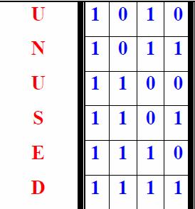
11 coded and the number is stored as 1001_0101_0111. Thus, we need a specific code for each of the 10 decimal digits. There is a variety of such decimal binary codes. The shown table gives several common such codes. One commonly used code is the Binary Coded Decimal (BCD) code which corresponds to the first 10 binary representations of the decimal digits 0-9. The BCD code requires 4 bits to represent the 10 decimal digits. Since 4 bits may have up to 16 different binary combinations, a total of 6 combinations will be unused. The position weights of the BCD code are 8, 4, 2, 1. Other codes (shown in the table) use position weights of 8, 4, -2, -1 and 2, 4, 2, 1. An example of a non-weighted code is the excess-3 code where digit codes is obtained from their binary equivalent after adding 3. Thus the code of a decimal 0 is 0011, that of 6 is 1001, etc.
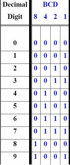
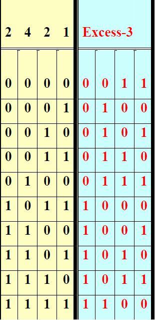

12
13 Gray Code The Gray code consist of 16 4-bit code words to represent the decimal Numbers 0 to 15. For Gray code, successive code words differ by only one bit from one to the next as shown in the table and further illustrated in the Figure
14 Character Codes ASCII Character Code ASCII code is a 7-bit code. Thus, it represents a total of 128 characters. Out of the 128 characters, there are 94 printable characters and 34 control (non- printable) characters. The printable characters include the upper and lower case letters (2*26), the 10 numerals (0-9), and 32 special characters, %, $, etc. For example, A is at (41)16, while a is at (61) )16. To convert upper case letters to lower case letters, add (20)16. Thus a is at (41)16 + (20)16 = (61)16. The code of the character 9 at position (39)16 is different from the binary number 9 ( ). To convert ASCII code of a numeral to its binary number value, subtract (30)16.
15 Boolean Algebra Boolean Algebra George Boole (1854) invented a new kind of algebra that could be used to analyse and design digital and computer circuits Boolean laws and theorems Certain rules and theorems are defined to facilitate the simplification of Boolean expressions inturn making the simpler logic circuits with reduced number of gates. Basic laws Commutative law: A+B =B+A AB = BA Associative law: A + (B+C) = (A+B) + C A(BC) = (AB)C
16 Distributive law: A (B+C) = AB + AC Postulates 1. Identity Identity elements exist for each operation that leaves the result unchanged. A+0 = A A.0 = 0 A+1 = 1 A.1 = A An operation between two identical variables will yield a result that is unchanged A+A = A A.A = A 2. Inverse For every element, there is an inverse or complement with the following properties A.A = 0 A+A = 1 3. The complement of a complement gives back the original quantity (A ) = A Boolean relations about OR operations
17 A+0=A A+A=A A+1=1 Boolean relations about AND operations A ' 1 = A A ' A = A A ' 0 = 0 DE MORGAN S THEOREMS 1. This states that the inverse (i.e.)of a product [and] is equal to the sum [or] of the complements 2. This states that the inverse (complement) of a sum [or] is equal to the product [and] of the complements These theorems can be extended to cover several variables: Logic Gates 1. NOT operation
18 Fig. 2-1: Inverter symbol and Boolean notation Ex: If A is 0 (low) ' X = NOT 0 = 1 In Boolean algebra the overbar stands for NOT operation. 2. OR operation TRUTH TABLE Fig. 2-2: OR symbol and Boolean notation Ex: If A = 0, B = 1 ' X = A or B = 0 or 1 = l In Boolean algebra the + sign stans for the OR A B Z X=A+B Ex: If A = 1, B = 0 ' X = A + B = = 1 3.AND operation
19 Fig. 2-3: AND symbol and Boolean notation In Boolean algebra the multiplication sign stands for the X = AB Ex: If A = 1, B = 0 ' X = A B = 1 ' 0 = 0 TRUTH TABLE A B Z AND operation 4. NOR gate Based on the three fundamental logic operations it is possible to design additionel logic devices. Fig. 2-6: NOR gate, symbol and truth table
20 5. NAND gate Fig. 2-7: NAND grate, symbol and truth table 6. XOR gate Events which are true only if and only if one of the motivating events are true Truth Table A B F Canonical and Standard forms Consider two binary variables x and y combined by an AND operation X. Y 0 0 m 0 X. Y 0 1 m 1
21 X. Y 1 0 m 2 Where X Primed representing binary 0 X. Y 1 1 m 3 And X Unprimed representing binary 1 m x Minterm or standard product For n variables, there are in total 2 n Minterms. For OR operation, X + Y 0 0 M 0 X + Y 0 1 M 1 X + Y 1 0 M 2 X + Y 1 1 M 3 M x Maxterm or standard sum Each Maxterm is the complement of corresponding Minterm. Boolean expression can be expressed in terms of Minterms and Maxterms as follows X Y Z f Sum of minterms: Boolean expression for the function f 1 from the given truth table is,
22 f 1 = X Y Z + XY Z + XYZ = m 1 + m 4 + m 7 ie) OR ing the minterms which gives 1 in the function f 1 2 Product of maxterms: Similarly, f 1 = (X+Y+Z) (X+Y +Z) (X+Y +Z ) (X +Y+Z ) (X +Y +Z) = M 0. M 2.M 3.M 5. M 6 ie) AND ing the maxterms which gives 0 in the function f 1 Karnaugh Map It is a systematic method to simplify Boolean expression using a map. Map is a diagram made up of cells where each cell gives the output value for the corresponding input combination. Totally there are 2 n cells for n input variables. The map presents a visual diagram of all possible ways a function may be expressed in a standard form. 1.Two- and Three- variable maps A Two-variable map is shown below. There are 4 cells for 2 variables. Each cell for a minterm. Figure (a) shows the minterms and (b) the relationship between the cells and variables. Example: F 1 = XY is represented by this mapping method as,
23 Since XY is equal to m 3, a 1 is placed inside the cell that belongs to m 3. Similarly, F 2 = X + Y as, A Three-variable map is shown below. Here 8 cells are not arranged in a binary sequence, but in a sequence similar to Gray code. The characteristic of this sequence is that only 1 bit changes from 0 to 1 or 1 to 0 in the listing sequence. ie) the minterms in the adjacent cells are differing by a single bit. This is the basic principle behind K-Map and can be clarified by taking a function having m 5 and m 7 as, m 5 + m 7 = XY Z + XYZ = XZ(Y +Y) = XZ.
24 Two minterms of 3 literals is solved into a single minterm of 2 literals. The two cells are considered to be adjacent even though they do not touch each other like m 0 and m 2. Example: #1) Simplify the Boolean function F(X, Y, Z) = (2, 3, 4, 5) Mark 1 in each minterm that represents the function. Find the adjacent cells (shown in two rectangles) Upper rectangle area is enclosed by the variables X and Y Similarly lower rectangle by variables X and Y So the resultant function is F(X, Y, Z) = (2, 3, 4, 5) = X Y + XY 2. Four- variable map A Four-variable map is shown below.
 and second column (01) gives 1101, the binary equivalent of decimal 13 representing m 13. The map minimization is the similar procedure as that of the three variable type.")
25 The minterm corresponding to each cell can be obtained by the concatenation of the respective row and column. For instance, third row (11) and second column (01) gives 1101, the binary equivalent of decimal 13 representing m 13. The map minimization is the similar procedure as that of the three variable type. No other combination of squares can simplify the function. 3.Five- variable map shown below Maps for more than 4 variables are not as simple to use. It needs 32 cells. A Five-variable map is It consists of 2 four-variable maps, where A distinguishes between two maps. Minterms 0 throgh 15 belong with A = 0 and Minterms 16 throgh 31 belong with A = 1. Each map retains adjacency when taken
26 separately. Each cell in the A = 0 map is adjacent to the corresponding cell in the A = 1 map like 4 and 20, 15 and 31. Simply, for 2 k adjacent squares, for k = 0,1,2..n, in an n-variable map will represent an area that gives a term of n-k literals. When n=k, the entire areas of the is combined to give the identity function. 4 Product of Sum simplification With minor modification, POS form is obtained as the result of simplification from the map. Simplified expression for the complement of the function,f, is obtained if the cells with 0 s are combined into valid squares. The complement of F inturn gives us F in POS form.(by Demorgan s Theorem) Ex: #1) Simplify the given Boolean expression in SOP and POS form. F(A,B,C,D) = (0,1,2,5,8,9,10)
27 Combining cells with 1 s gives the SOP form, F = B D + B C + A C D Combining cells with 0 s gives the form, F = AB + CD + BD Applyind Demorgan s theorem, we get the simplified POS form F = (A + B ) (C + D ) (B + D) Gate implementation of the function F = B D + B C + A C D F = (A + B ) (C + D ) (B + D) NAND and NOR Implementation NAND and NOR gates are easier to fabricate and are the basic gates used in all IC digital logic families. So Boolean functions interms of NAND and NOR is necessory. The invert OR symbol is followed from the Demorgan s thoerem. Similarly for NOR gate,
28 A one-input NAND or NOR behaves like an inverter 1. NAND implementation Boolean expression in sum of product form is needed for NAND implementation. Consider for example, F = AB+CD+E is implemented in three ways as shown below. Figure (a) and (c) looks similar but NAND implementation needs one more NAND gate for complementing E. By Demorgan s theorem, F = [ (AB). (CD). E ] = AB + CD + E. Thus the two level implementation is possible with the NAND gates for the given Boolean expression.
29 2. NOR implementation NOR function is the dual of the NAND function. So all the procedures and rules for NOR logic are the dual of the NAND logic. Boolean expression in product of sum form is needed for NOR implementation. For the same example given above, F = (A+B). (C+D). E To obtain product of sum from a map, it is necessary to combine cells with 0 s and then complement the function. 3. Don t-care conditions The logical sun of minterms associated with the Boolean function specifies the condition under which the function is equal to 1. The function is equal to 0 for the rest of the minterms. Ie) all the combinations of variables are valid. In some practical applications the function is not specified for certain combinations of variables. For example four bit codes for BCD greater than 9 has six invalid combinations. These unspecified minterms are known as don t care conditions and used for further simplification. To distinguish don t care condition from 0 and 1, it is marked with X. Don t care cell is assumed to be 1 or 0 when choosing adjacent squares. Ex. #1) Simplify F(w,x,y,z) = (1,3,7,11,15) That has the don t care conditions d(w,x,y,z) = (0,2,5)
30 All the five 1 s should be included to form the sum of products. But X may or may not be included. By including 0 and 2 don t care items, F = yz+w x By including 5 don t care item, F = yz+w z Expression in POS form is by grouping 0 s and include minterms 0 and 2 to get it in the simplified version. F = z + wy Complementing F yields F(w,x,y,z) = z(w +y) = yz+w z For this case minterms 0 and 2 are included with 0 s and minterm 5 with the 1 s. TABULATION METHOD If the number of variables exceeds five or six, excessive number of cells make the grouping difficult whereby the tabulation method is a step-by-step procedure.this method was first tabulated by Quine and later improved by Mccluskey. Hence it is known as Quine- Mccluskey method. It consists of two parts. First is to find the Prime implicants. Second to choose among the prime implicants those that give an expression with least number of literals. Example 1) Find minimal SOP for f = (1,2,3,4,5,7,8,9,10,11,14,15)
31 Solution: i) write the given minterms in binary form minterms A B C D ii) Arrange the numbers in increasing number of 1 s No. Of 1 s minterms A B C D 1 ^ ^ ^ ^ ^ ^ ^ ^ ^ ^
32 4 15 ^ iii) Compare adjacent groups to find numbers which differ by 1 variable. ^denotes the numbers undergone the comparision Combination A B C D (1,3) ^ 0 0 _ 1 (1,9)^ _ (2,3)^ _ (2,10)^ _ (8,9)^ _ (8,10) ^ 1 0 _ 0 (3,7)^ 0 _ 1 1 (3,11)^ _ (9,11)^ 1 0 _ 1 (10,11)^ _ (10,14) ^ 1 _ 1 0 (7,15) ^ _ (11,15)^ 1 _ 1 1 (14,15)^ denotes the differing variable position iv) Form 4 cell combination,by having adjacent group comparison, with 1 bit varying and _ in same position Combination A B C D (1,3,9,11) _ 0 _ 1 (2,3,10,11) _ 0 1 _ (8,9,10,11) 1 0
33 (3,7,11,15) 1 1 (10,11,14,15) 1 _ 1 _ From the above table no more combination is possible. v) Prime Implicants table Prime Implicants (1,3,9,11)* X X X X (2,3,10,11)* X X X X (8,9,10,11)* X X X X (3,7,11,15)* X X X X (10,11,14,15)* X X X X Essential ^ ^ ^ Prime Implicants ^ ^ Essential Prime Implicants is the one which has only one X in the column of minterms * mark is placed on the Prime Implicants which has Essential Prime Implicants inside. The resultant function consisting of Essential Prime Implicants and the Prime Implicants covering the remaining minterms. Here all the Prime Implicants are Essential Prime Implicants. Therefore Y = B D + B C + AB + CD + AC SUMMARY Digital electronics are electronics systems that use digital signals. Arithmetic in binary is much like arithmetic in other numeral systems. Addition, subtraction, multiplication, and division can be performed on binary numerals. One commonly used code is the Binary Coded Decimal (BCD) code non-weighted code is the excess-3 code where digit codes is obtained from their binary equivalent after adding 3.
34 Gray code consist of 16 4-bit code words to represent the decimal Numbers 0 to 15. ASCII code is a 7-bit Alpha-Numeric code Karnaugh Map is a systematic method to simplify Boolean expression using a map. KEY TERM Binary codes De morgan s theorems Product of maxterms Logic Gates ASCII Sum of minterms Karnaugh Map Universal Gates MULTIPLE CHOICE 1)Digital signals: (a) vary smoothly, then change abruptly to new values. (b) consist of codes of high-level and low-level signals. (c) vary smoothly continuously. (d) have periods of high-level and low-level signals, then change to continuous signals. 2)Binary digital systems: (a) have two discrete levels 1 or 0, high level or low level. (b) have three or more discrete levels. (c) have a level that varies continuously with time. (d) have binary digits, or bits for short. (e) none of the above. (f) d and a above. 3)Decimal numbering systems have: (a) weighted digit positions that vary randomly. (b) weighted digit positions varying by powers of 10. (c) weighted digit positions varying by powers of 2. (d) weighted digit positions that remain constant at one value.
35 4)Digital systems represent quantities: (a) using combinations of binary digits in codes. (b) using more bits in its binary codes as the quantity value increases. (c) using more bits in its binary code as more accuracy is required. (d) using binary codes with just two levels 1 or 0, high level or low level. (e) none of the above. (f) all of the above. 5) The standard SOP form of the expression is (a) (b) (c) (d) 6) The standard symbol for EX-OR gate is 7) In the 8421 BCD code the decimal number 125 is written as a) b) c) 7D d) None of the above 8) The expression can be simplified to
36 9) The 2's complement of is 10) Number of nibbles making one byte is 11) Next binary number after 0,1, 10, 11 is - 12)
37 13)The binary division gives 14) The binary equivalent of is 15) The output Y of the circuit in the given figure is
38 PART-A 1. Find the hexadecimal equivalent of the decimal number Find the octal equivalent of the decimal number What is meant by weighted and non-weighted coding? 4. Convert A3BH and 2F3H into binary and octal respectively 5. Find the decimal equivalent of (123)9 6. Find the octal equivalent of the hexadecimal number AB.CD 7. Encode the ten decimal digits in the 2 out of 5 code 8. Show that the Excess 3 code is self complementing 9. Find the hexadecimal equivalent of the octal number Find the decimal equivalent of (346)7 11. A hexadecimal counter capable of counting up to at least (10,000)10 is to be constructed. What is the minimum number of hexadecimal digits that the counter must have? 12. Convert the decimal number 214 to hexadecimal 13. Convert to base Give an example of a switching function that contains only cyclic prime implicant 15. Give an example of a switching function that for which the MSP from is not unique. 16. Express x+yz as the sum of minterms 17. What is prime implicant? 18. Find the value of X = A B C (A+D) if A=0; B=1; C=1 and D=1 19. What are minterms and maxterms? 20. State and prove Demorgan s theorem 21. Find the complement of x+yz 22. Define the following : minterm and term 23. State and prove Consensus theorem 24. What theorem is used when two terms in adjacent squares of K map are combined? 25. How will you use a 4 input NAND gate as a 2 input NAND gate? 26. How will you use a 4 input NOR gate as a 2 input NOR gate? 27. Show that the NAND connection is not associative 28. What happens when all the gates is a two level AND-OR gate network are replaced by NOR gates? 29. What is meant by multilevel gates networks? 30. Show that the NAND gate is a universal building block
39 PART-B 1. (a) Explain how you will construct an (n+1) bit Gray code from an n bit Gray code (b) Show that the Excess 3 code is self -complementing 2. (a) Prove that (x1+x2).(x1. x3 +x3) (x2 + x1.x3) =x1 x2 (b) Simplify using K-map to obtain a minimum POS expression: (A + B +C+D) (A+B +C+D) (A+B+C+D ) (A+B+C +D ) (A +B+C +D ) (A+B+C +D) 3. (a) State and Prove idempotent laws of Boolean algebra. (b) using a K-Map,Find the MSP from of F= _(0,4,8,12,3,7,11,15) +_d(5) 4. Find the Minterm expansion of f(a,b,c,d) = a (b +d) + acd 5. Simplify the following Boolean function by using the Tabulation Method F= _ (0, 1, 2, 8, 10, 11, 14, 15) 6. State and Prove the postulates of Boolean algebra 7. Find a Min SOP and Min POS for f = b c d + bcd + acd + a b c + a bc d 8. State and Prove the theorems of Boolean algebra with illustration 9. Find the MSP representation for F(A,B,C,D,E) = _m(1,4,6,10,20,22,24,26) + _d (0,11,16,27) using K-Map method Draw the circuit of the minimal expression using only NAND gates 10. (a) Show that if all the gates in a two level AND-OR gate networks are replaced by NAND gates the output function does not change (b) Why does a good logic designer minimize the use of NOT gates?
40
41 Appendix-I IC s 74LS00 Quad 2 input NAND gate 74LS01 Quad 2 input NAND gate (OC) 74LS02 Quad 2 input NOR gate 74LS03 Quad 2 input NAND gate 74LS04 74LS05 74LS06 74LS08 74LS09 74LS10 74LS11 74LS12 74LS13 74LS14 74LS16 74LS15 74LS20 74LS21 Hex Inverter Hex Inverter (OC) Hex Inverter buffer/driver Quad 2 input AND Quad 2 input AND gate (OC) Triple 3 input NAND gate Triple 3 input AND gate Triple 3 input NAND gate (OC) Dual 4-input NAND gate Schmitt trigger Hex Inverter Schmitt trigger Hex Inverter (OC) Triple 3 input AND gate (OC) Dual 4 input NAND gate Dual 4 input AND gate
42 74LS22 Dual 4 input NAND gate (OC) 7425 Dual 4 input NOR gate with strobe 74LS22 Dual 4 input NAND gate (OC) 7425 Dual 4 input NOR gate with strobe 74LS27 74LS30 74LS32 74LS38 74LS42 Triple 3 input NOR gate 8 input NAND gate Quad 2 input OR gate Quad 2 input NAND gate Buffer BCD to DEC decoder 7445 BCD to DEC decoder 74LS47 74LS48 74LS51 74LS54 74F64 BCD to 7 seg decoder/driver BCD to 7 seg decoder/driver AND/OR/INVERT gate AND/OR/INVERT gate AND/OR/INVERT gate 7470 JK flip flop 7472 JK M/S flip flop 74LS73 74LS74 74LS75 Dual JK flip flop with clear Dual D-Type flip-flops with preset and clear 4 bit bistable latch
43 74LS76 74LS83 74LS85 74LS86 74LS90 74LS91 74LS92 74LS93 74LS95 Dual JK flip-flops with preset and clear 4 bit full adder 4 bit magnitude comparator Quad 2 input XOR gate Decade counter 8-bit shift register Divide by 12 counter Binary counter 4 bit shift register 74LS107 Dual JK flip-flops with clear 74LS109 Dual JK pos edge trig flip flop 74LS112 Dual JK neg edge trig flip flop Monostable multivibrator 74LS122 Monostable multivibrator 74LS123 Monostable multivibrator 74LS125 Monostable multivibrator 74LS132 Quad 2 input NAND gate Schmitt trigger 74S input NAND 74LS136 Quad 2 input XOR (O.C) 74LS138 3-to-8 line decoder/demux
44 74LS139 Dual 1-of-4 decoder/demux 74LS line - 4 line octal priority encoder 74LS148 8 line - 3 line octal priority encoder Data selector/mux 74LS151 8 input MUX 74LS153 Dual 4-to-1 Multiplexer 74LS154 4-to16 decoder/demux 74LS155 Dual 2 line to 4 line decoder / demux 74LS156 Dual 2 line to 4 line decoder / demux (O.C) 74LS157 Quad 2 input MUX 74LS158 Quad 2 input MUX with invereted outputs 74LS160 BCD decade counter 74LS161 Synchronous 4 bit binary counter 74LS162 BCD decade counter counter 74LS163 Asynchronous 4 bit binary counter 74LS164 8 bit SIPO shift register 74LS165 8 bit PISO shift register 74LS166 74LS174 74LS175 8 bit PISO shift register Hex D type flip flop with clear Quad D type flip flop with clear
45 74176 Decade Counter Binary Counter 74LS191 74LS192 74LS193 74LS195 74LS196 74LS197 4 bit binary up / down counter BCD up / down counter 4 bit binary up / down counter 4 bit shift register Presettable decade counter Presettable binary counter bit shift register 74LS221 74S225 74LS240 74LS241 74LS244 74LS245 74LS251 74LS257 74LS259 74LS266 74LS273 Dual monostable multivibrator 16x5 FIFO memory Octal buffer/line driver Octal 3-state buffer Octal buffer/line driver Octal bus transceiver Data selector / MUX Quad 2 input mux 3-state 8 bit addressable latch Quad 2 input XNOR (O.C) Octal D type flip flop with clear
46 74LS280 74LS298 74LS299 74LS323 74LS367 74LS368 74LS373 74LS374 74LS390 74LS393 74LS395 74LS540 74LS541 9 bit odd / even parity generator Quad 2 input MUX with storage 8 bit universal shift register 8-Bit Shift register Hex bus driver Hex bus driver with inverters Octal transparent latch Octal D type flip flop 3-state Dual 4 bit decade counter Dual 4 bit binary counter 4 bit shift register Octal buffer 3-state Octal buffer 3-state outputs
 Get Free notes at Module-I One s Complement: Complement all the bits.i.e. makes all 1s as 0s and all 0s as 1s Two s Complement: One s complement+1 SIGNED BINARY NUMBERS Positive integers (including zero)
Gate Level Minimization Map Method
 Gate Level Minimization Map Method Complexity of hardware implementation is directly related to the complexity of the algebraic expression Truth table representation of a function is unique Algebraically
Injntu.com Injntu.com Injntu.com R16
 1. a) What are the three methods of obtaining the 2 s complement of a given binary (3M) number? b) What do you mean by K-map? Name it advantages and disadvantages. (3M) c) Distinguish between a half-adder
IT 201 Digital System Design Module II Notes
 IT 201 Digital System Design Module II Notes BOOLEAN OPERATIONS AND EXPRESSIONS Variable, complement, and literal are terms used in Boolean algebra. A variable is a symbol used to represent a logical quantity.
VALLIAMMAI ENGINEERING COLLEGE. SRM Nagar, Kattankulathur DEPARTMENT OF ELECTRONICS AND COMMUNICATION ENGINEERING EC6302 DIGITAL ELECTRONICS
 VALLIAMMAI ENGINEERING COLLEGE SRM Nagar, Kattankulathur-603 203 DEPARTMENT OF ELECTRONICS AND COMMUNICATION ENGINEERING EC6302 DIGITAL ELECTRONICS YEAR / SEMESTER: II / III ACADEMIC YEAR: 2015-2016 (ODD
B.Tech II Year I Semester (R13) Regular Examinations December 2014 DIGITAL LOGIC DESIGN
 Regular Examinations December 2014 DIGITAL LOGIC DESIGN") B.Tech II Year I Semester () Regular Examinations December 2014 (Common to IT and CSE) (a) If 1010 2 + 10 2 = X 10, then X is ----- Write the first 9 decimal digits in base 3. (c) What is meant by don
B.Tech II Year I Semester () Regular Examinations December 2014 (Common to IT and CSE) (a) If 1010 2 + 10 2 = X 10, then X is ----- Write the first 9 decimal digits in base 3. (c) What is meant by don
VALLIAMMAI ENGINEERING COLLEGE
 VALLIAMMAI ENGINEERING COLLEGE SRM Nagar, Kattankulathur 603 203 DEPARTMENT OF INFORMATION TECHNOLOGY & COMPUTER SCIENCE AND ENGINEERING QUESTION BANK II SEMESTER CS6201- DIGITAL PRINCIPLE AND SYSTEM DESIGN
1. Mark the correct statement(s)
") 1. Mark the correct statement(s) 1.1 A theorem in Boolean algebra: a) Can easily be proved by e.g. logic induction b) Is a logical statement that is assumed to be true, c) Can be contradicted by another
1. Mark the correct statement(s) 1.1 A theorem in Boolean algebra: a) Can easily be proved by e.g. logic induction b) Is a logical statement that is assumed to be true, c) Can be contradicted by another
CHAPTER-2 STRUCTURE OF BOOLEAN FUNCTION USING GATES, K-Map and Quine-McCluskey
 CHAPTER-2 STRUCTURE OF BOOLEAN FUNCTION USING GATES, K-Map and Quine-McCluskey 2. Introduction Logic gates are connected together to produce a specified output for certain specified combinations of input
Gate-Level Minimization. BME208 Logic Circuits Yalçın İŞLER
 Gate-Level Minimization BME28 Logic Circuits Yalçın İŞLER islerya@yahoo.com http://me.islerya.com Complexity of Digital Circuits Directly related to the complexity of the algebraic expression we use to
DIGITAL SYSTEM DESIGN
 DIGITAL SYSTEM DESIGN UNIT I: Introduction to Number Systems and Boolean Algebra Digital and Analog Basic Concepts, Some history of Digital Systems-Introduction to number systems, Binary numbers, Number
Digital logic fundamentals. Question Bank. Unit I
 Digital logic fundamentals Question Bank Subject Name : Digital Logic Fundamentals Subject code: CA102T Staff Name: R.Roseline Unit I 1. What is Number system? 2. Define binary logic. 3. Show how negative
END-TERM EXAMINATION
 (Please Write your Exam Roll No. immediately) END-TERM EXAMINATION DECEMBER 2006 Exam. Roll No... Exam Series code: 100919DEC06200963 Paper Code: MCA-103 Subject: Digital Electronics Time: 3 Hours Maximum
Code No: 07A3EC03 Set No. 1
 Code No: 07A3EC03 Set No. 1 II B.Tech I Semester Regular Examinations, November 2008 SWITCHING THEORY AND LOGIC DESIGN ( Common to Electrical & Electronic Engineering, Electronics & Instrumentation Engineering,
3. The high voltage level of a digital signal in positive logic is : a) 1 b) 0 c) either 1 or 0
 1 b) 0 c) either 1 or 0") 1. The number of level in a digital signal is: a) one b) two c) four d) ten 2. A pure sine wave is : a) a digital signal b) analog signal c) can be digital or analog signal d) neither digital nor analog
1. The number of level in a digital signal is: a) one b) two c) four d) ten 2. A pure sine wave is : a) a digital signal b) analog signal c) can be digital or analog signal d) neither digital nor analog
SWITCHING THEORY AND LOGIC CIRCUITS
 SWITCHING THEORY AND LOGIC CIRCUITS COURSE OBJECTIVES. To understand the concepts and techniques associated with the number systems and codes 2. To understand the simplification methods (Boolean algebra
Code No: R Set No. 1
 Code No: R059210504 Set No. 1 II B.Tech I Semester Supplementary Examinations, February 2007 DIGITAL LOGIC DESIGN ( Common to Computer Science & Engineering, Information Technology and Computer Science
Combinational Logic & Circuits
 Week-I Combinational Logic & Circuits Spring' 232 - Logic Design Page Overview Binary logic operations and gates Switching algebra Algebraic Minimization Standard forms Karnaugh Map Minimization Other
CS8803: Advanced Digital Design for Embedded Hardware
 CS883: Advanced Digital Design for Embedded Hardware Lecture 2: Boolean Algebra, Gate Network, and Combinational Blocks Instructor: Sung Kyu Lim (limsk@ece.gatech.edu) Website: http://users.ece.gatech.edu/limsk/course/cs883
 Class Subject Code Subject Prepared By Lesson Plan for Time: Lesson. No 1.CONTENT LIST: Introduction to UnitI 2. SKILLS ADDRESSED: Listening I year, 02 sem CS6201 Digital Principles & System Design S.Seedhanadevi
SUBJECT CODE: IT T35 DIGITAL SYSTEM DESIGN YEAR / SEM : 2 / 3
 UNIT - I PART A (2 Marks) 1. Using Demorgan s theorem convert the following Boolean expression to an equivalent expression that has only OR and complement operations. Show the function can be implemented
 www.vidyarthiplus.com Question Paper Code : 31298 B.E./B.Tech. DEGREE EXAMINATION, NOVEMBER/DECEMBER 2013. Third Semester Computer Science and Engineering CS 2202/CS 34/EC 1206 A/10144 CS 303/080230012--DIGITAL
ELCT201: DIGITAL LOGIC DESIGN
 ELCT201: DIGITAL LOGIC DESIGN Dr. Eng. Haitham Omran, haitham.omran@guc.edu.eg Dr. Eng. Wassim Alexan, wassim.joseph@guc.edu.eg Lecture 3 Following the slides of Dr. Ahmed H. Madian محرم 1439 ه Winter
COPYRIGHTED MATERIAL INDEX
 INDEX Absorption law, 31, 38 Acyclic graph, 35 tree, 36 Addition operators, in VHDL (VHSIC hardware description language), 192 Algebraic division, 105 AND gate, 48 49 Antisymmetric, 34 Applicable input
Chapter 2. Boolean Expressions:
 Chapter 2 Boolean Expressions: A Boolean expression or a function is an expression which consists of binary variables joined by the Boolean connectives AND and OR along with NOT operation. Any Boolean
Code No: R Set No. 1
 Code No: R059210504 Set No. 1 II B.Tech I Semester Regular Examinations, November 2006 DIGITAL LOGIC DESIGN ( Common to Computer Science & Engineering, Information Technology and Computer Science & Systems
2008 The McGraw-Hill Companies, Inc. All rights reserved.
 28 The McGraw-Hill Companies, Inc. All rights reserved. 28 The McGraw-Hill Companies, Inc. All rights reserved. All or Nothing Gate Boolean Expression: A B = Y Truth Table (ee next slide) or AB = Y 28
10EC33: DIGITAL ELECTRONICS QUESTION BANK
 10EC33: DIGITAL ELECTRONICS Faculty: Dr.Bajarangbali E Examination QuestionS QUESTION BANK 1. Discuss canonical & standard forms of Boolean functions with an example. 2. Convert the following Boolean function
R10. II B. Tech I Semester, Supplementary Examinations, May
 SET - 1 1. a) Convert the following decimal numbers into an equivalent binary numbers. i) 53.625 ii) 4097.188 iii) 167 iv) 0.4475 b) Add the following numbers using 2 s complement method. i) -48 and +31
DHANALAKSHMI SRINIVASAN COLLEGE OF ENGINEERING AND TECHNOLOGY
 DHANALAKSHMI SRINIVASAN COLLEGE OF ENGINEERING AND TECHNOLOGY Dept/Sem: II CSE/03 DEPARTMENT OF ECE CS8351 DIGITAL PRINCIPLES AND SYSTEM DESIGN UNIT I BOOLEAN ALGEBRA AND LOGIC GATES PART A 1. How many
VALLIAMMAI ENGINEERING COLLEGE
 VALLIAMMAI ENGINEERING COLLEGE SRM Nagar, Kattankulathur 603 203 DEPARTMENT OF INFORMATION TECHNOLOGY QUESTION BANK Academic Year 2018 19 III SEMESTER CS8351-DIGITAL PRINCIPLES AND SYSTEM DESIGN Regulation
ELCT201: DIGITAL LOGIC DESIGN
 ELCT201: DIGITAL LOGIC DESIGN Dr. Eng. Haitham Omran, haitham.omran@guc.edu.eg Dr. Eng. Wassim Alexan, wassim.joseph@guc.edu.eg Lecture 3 Following the slides of Dr. Ahmed H. Madian ذو الحجة 1438 ه Winter
2.1 Binary Logic and Gates
 1 EED2003 Digital Design Presentation 2: Boolean Algebra Asst. Prof.Dr. Ahmet ÖZKURT Asst. Prof.Dr Hakkı T. YALAZAN Based on the Lecture Notes by Jaeyoung Choi choi@comp.ssu.ac.kr Fall 2000 2.1 Binary
Chapter 3. Gate-Level Minimization. Outlines
 Chapter 3 Gate-Level Minimization Introduction The Map Method Four-Variable Map Five-Variable Map Outlines Product of Sums Simplification Don t-care Conditions NAND and NOR Implementation Other Two-Level
Module -7. Karnaugh Maps
 1 Module -7 Karnaugh Maps 1. Introduction 2. Canonical and Standard forms 2.1 Minterms 2.2 Maxterms 2.3 Canonical Sum of Product or Sum-of-Minterms (SOM) 2.4 Canonical product of sum or Product-of-Maxterms(POM)
Code No: R Set No. 1
 Code No: R059210504 Set No. 1 II B.Tech I Semester Regular Examinations, November 2007 DIGITAL LOGIC DESIGN ( Common to Computer Science & Engineering, Information Technology and Computer Science & Systems
Scheme G. Sample Test Paper-I
 Sample Test Paper-I Marks : 25 Times:1 Hour 1. All questions are compulsory. 2. Illustrate your answers with neat sketches wherever necessary. 3. Figures to the right indicate full marks. 4. Assume suitable
Experiment 4 Boolean Functions Implementation
 Experiment 4 Boolean Functions Implementation Introduction: Generally you will find that the basic logic functions AND, OR, NAND, NOR, and NOT are not sufficient to implement complex digital logic functions.
Simplification of Boolean Functions
 Simplification of Boolean Functions Contents: Why simplification? The Map Method Two, Three, Four and Five variable Maps. Simplification of two, three, four and five variable Boolean function by Map method.
Principles of Digital Techniques PDT (17320) Assignment No State advantages of digital system over analog system.
 Assignment No State advantages of digital system over analog system.") Assignment No. 1 1. State advantages of digital system over analog system. 2. Convert following numbers a. (138.56) 10 = (?) 2 = (?) 8 = (?) 16 b. (1110011.011) 2 = (?) 10 = (?) 8 = (?) 16 c. (3004.06)
Assignment No. 1 1. State advantages of digital system over analog system. 2. Convert following numbers a. (138.56) 10 = (?) 2 = (?) 8 = (?) 16 b. (1110011.011) 2 = (?) 10 = (?) 8 = (?) 16 c. (3004.06)
LSN 4 Boolean Algebra & Logic Simplification. ECT 224 Digital Computer Fundamentals. Department of Engineering Technology
 LSN 4 Boolean Algebra & Logic Simplification Department of Engineering Technology LSN 4 Key Terms Variable: a symbol used to represent a logic quantity Compliment: the inverse of a variable Literal: a
Unit-IV Boolean Algebra
 Unit-IV Boolean Algebra Boolean Algebra Chapter: 08 Truth table: Truth table is a table, which represents all the possible values of logical variables/statements along with all the possible results of
UNIT-4 BOOLEAN LOGIC. NOT Operator Operates on single variable. It gives the complement value of variable.
 UNIT-4 BOOLEAN LOGIC Boolean algebra is an algebra that deals with Boolean values((true and FALSE). Everyday we have to make logic decisions: Should I carry the book or not?, Should I watch TV or not?
Logic design Ibn Al Haitham collage /Computer science Eng. Sameer
 DEMORGAN'S THEOREMS One of DeMorgan's theorems stated as follows: The complement of a product of variables is equal to the sum of the complements of the variables. DeMorgan's second theorem is stated as
BHARATHIDASAN ENGINEERING COLLEGE Degree / Branch : B.E./ECE Year / Sem : II/ III Sub.Code / Name : EC6302/DIGITAL ELECTRONICS
 BHARATHIDASAN ENGINEERING COLLEGE Degree / Branch : B.E./ECE Year / Sem : II/ III Sub.Code / Name : EC6302/DIGITAL ELECTRONICS FREQUENTLY ASKED QUESTIONS UNIT I MINIMIZATION TECHNIQUES AND LOGIC GATES
SIDDHARTH GROUP OF INSTITUTIONS :: PUTTUR Siddharth Nagar, Narayanavanam Road QUESTION BANK (DESCRIPTIVE)
") SIDDHARTH GROUP OF INSTITUTIONS :: PUTTUR Siddharth Nagar, Narayanavanam Road 517583 QUESTION BANK (DESCRIPTIVE) Subject with Code : STLD(16EC402) Year & Sem: II-B.Tech & I-Sem Course & Branch: B.Tech
SIDDHARTH GROUP OF INSTITUTIONS :: PUTTUR Siddharth Nagar, Narayanavanam Road 517583 QUESTION BANK (DESCRIPTIVE) Subject with Code : STLD(16EC402) Year & Sem: II-B.Tech & I-Sem Course & Branch: B.Tech
R07. Code No: V0423. II B. Tech II Semester, Supplementary Examinations, April
 SET - 1 II B. Tech II Semester, Supplementary Examinations, April - 2012 SWITCHING THEORY AND LOGIC DESIGN (Electronics and Communications Engineering) Time: 3 hours Max Marks: 80 Answer any FIVE Questions
UNIT II. Circuit minimization
 UNIT II Circuit minimization The complexity of the digital logic gates that implement a Boolean function is directly related to the complexity of the algebraic expression from which the function is implemented.
Combinational Logic Circuits
 Chapter 2 Combinational Logic Circuits J.J. Shann (Slightly trimmed by C.P. Chung) Chapter Overview 2-1 Binary Logic and Gates 2-2 Boolean Algebra 2-3 Standard Forms 2-4 Two-Level Circuit Optimization
Chapter 2 Boolean algebra and Logic Gates
 Chapter 2 Boolean algebra and Logic Gates 2. Introduction In working with logic relations in digital form, we need a set of rules for symbolic manipulation which will enable us to simplify complex expressions
CONTENTS CHAPTER 1: NUMBER SYSTEM. Foreword...(vii) Preface... (ix) Acknowledgement... (xi) About the Author...(xxiii)
 Preface... (ix) Acknowledgement... (xi) About the Author...(xxiii)") CONTENTS Foreword...(vii) Preface... (ix) Acknowledgement... (xi) About the Author...(xxiii) CHAPTER 1: NUMBER SYSTEM 1.1 Digital Electronics... 1 1.1.1 Introduction... 1 1.1.2 Advantages of Digital Systems...
CONTENTS Foreword...(vii) Preface... (ix) Acknowledgement... (xi) About the Author...(xxiii) CHAPTER 1: NUMBER SYSTEM 1.1 Digital Electronics... 1 1.1.1 Introduction... 1 1.1.2 Advantages of Digital Systems...
Gate-Level Minimization
 MEC520 디지털공학 Gate-Level Minimization Jee-Hwan Ryu School of Mechanical Engineering Gate-Level Minimization-The Map Method Truth table is unique Many different algebraic expression Boolean expressions may
D I G I T A L C I R C U I T S E E
 D I G I T A L C I R C U I T S E E Digital Circuits Basic Scope and Introduction This book covers theory solved examples and previous year gate question for following topics: Number system, Boolean algebra,
INSTITUTE OF AERONAUTICAL ENGINEERING (Autonomous) Dundigal, Hyderabad
 Dundigal, Hyderabad") INSTITUTE OF AERONAUTICAL ENGINEERING (Autonomous) Dundigal, Hyderabad - 500 043 COMPUTER SCIENCE AND ENGINEERING TUTORIAL QUESTION BANK Name : DIGITAL LOGIC DESISN Code : AEC020 Class : B Tech III Semester
INSTITUTE OF AERONAUTICAL ENGINEERING (Autonomous) Dundigal, Hyderabad - 500 043 COMPUTER SCIENCE AND ENGINEERING TUTORIAL QUESTION BANK Name : DIGITAL LOGIC DESISN Code : AEC020 Class : B Tech III Semester
Chapter 2 Combinational Logic Circuits
 Logic and Computer Design Fundamentals Chapter 2 Combinational Logic Circuits Part 2 Circuit Optimization Overview Part Gate Circuits and Boolean Equations Binary Logic and Gates Boolean Algebra Standard
HANSABA COLLEGE OF ENGINEERING & TECHNOLOGY (098) SUBJECT: DIGITAL ELECTRONICS ( ) Assignment
 SUBJECT: DIGITAL ELECTRONICS ( ) Assignment") Assignment 1. What is multiplexer? With logic circuit and function table explain the working of 4 to 1 line multiplexer. 2. Implement following Boolean function using 8: 1 multiplexer. F(A,B,C,D) = (2,3,5,7,8,9,12,13,14,15)
Assignment 1. What is multiplexer? With logic circuit and function table explain the working of 4 to 1 line multiplexer. 2. Implement following Boolean function using 8: 1 multiplexer. F(A,B,C,D) = (2,3,5,7,8,9,12,13,14,15)
DIGITAL ELECTRONICS. Vayu Education of India
 DIGITAL ELECTRONICS ARUN RANA Assistant Professor Department of Electronics & Communication Engineering Doon Valley Institute of Engineering & Technology Karnal, Haryana (An ISO 9001:2008 ) Vayu Education
2.6 BOOLEAN FUNCTIONS
 2.6 BOOLEAN FUNCTIONS Binary variables have two values, either 0 or 1. A Boolean function is an expression formed with binary variables, the two binary operators AND and OR, one unary operator NOT, parentheses
MGU-BCA-205- Second Sem- Core VI- Fundamentals of Digital Systems- MCQ s. 2. Why the decimal number system is also called as positional number system?
 MGU-BCA-205- Second Sem- Core VI- Fundamentals of Digital Systems- MCQ s Unit-1 Number Systems 1. What does a decimal number represents? A. Quality B. Quantity C. Position D. None of the above 2. Why the
INSTITUTE OF AERONAUTICAL ENGINEERING (Autonomous) Dundigal, Hyderabad
 Dundigal, Hyderabad") INSTITUTE OF AERONAUTICAL ENGINEERING (Autonomous) Dundigal, Hyderabad - 500043 Course Name : DIGITAL LOGIC DESISN Course Code : AEC020 Class : B Tech III Semester Branch : CSE Academic Year : 2018 2019
INSTITUTE OF AERONAUTICAL ENGINEERING (Autonomous) Dundigal, Hyderabad - 500043 Course Name : DIGITAL LOGIC DESISN Course Code : AEC020 Class : B Tech III Semester Branch : CSE Academic Year : 2018 2019
Boolean Algebra and Logic Gates
 Boolean Algebra and Logic Gates Binary logic is used in all of today's digital computers and devices Cost of the circuits is an important factor Finding simpler and cheaper but equivalent circuits can
Assignment (3-6) Boolean Algebra and Logic Simplification - General Questions
 Boolean Algebra and Logic Simplification - General Questions") Assignment (3-6) Boolean Algebra and Logic Simplification - General Questions 1. Convert the following SOP expression to an equivalent POS expression. 2. Determine the values of A, B, C, and D that make
Assignment (3-6) Boolean Algebra and Logic Simplification - General Questions 1. Convert the following SOP expression to an equivalent POS expression. 2. Determine the values of A, B, C, and D that make
Number Systems UNIT. Learning Objectives. 1.0 Introduction
 UNIT 1 Number Systems Learning Objectives To study Binary, Octal, Hexadecimal, Decimal number systems. Conversion of Binary to Octal, Binary to decimal, Binary to Hexa decimal and Conversion. Binary Addition,
UNIT I BOOLEAN ALGEBRA AND COMBINATIONAL CIRCUITS PART-A (2 MARKS)
") SUBJECT NAME: DIGITAL LOGIC CIRCUITS YEAR / SEM : II / III DEPARTMENT : EEE UNIT I BOOLEAN ALGEBRA AND COMBINATIONAL CIRCUITS 1. What is variable mapping? 2. Name the two canonical forms for Boolean algebra.
SUBJECT NAME: DIGITAL LOGIC CIRCUITS YEAR / SEM : II / III DEPARTMENT : EEE UNIT I BOOLEAN ALGEBRA AND COMBINATIONAL CIRCUITS 1. What is variable mapping? 2. Name the two canonical forms for Boolean algebra.
NH 67, Karur Trichy Highways, Puliyur C.F, Karur District UNIT-II COMBINATIONAL CIRCUITS
 NH 67, Karur Trichy Highways, Puliyur C.F, 639 114 Karur District DEPARTMENT OF ELETRONICS AND COMMUNICATION ENGINEERING COURSE NOTES SUBJECT: DIGITAL ELECTRONICS CLASS: II YEAR ECE SUBJECT CODE: EC2203
COLLEGE OF ENGINEERING DEPARTMENT OF ELECTRICAL AND ELECTRONICS ENGINEERING QUESTION BANK SUBJECT CODE & NAME: EC 1312 DIGITAL LOGIC CIRCUITS UNIT I
 KINGS COLLEGE OF ENGINEERING DEPARTMENT OF ELECTRICAL AND ELECTRONICS ENGINEERING QUESTION BANK SUBJECT CODE & NAME: EC 1312 DIGITAL LOGIC CIRCUITS YEAR / SEM: III / V UNIT I NUMBER SYSTEM & BOOLEAN ALGEBRA
NODIA AND COMPANY. GATE SOLVED PAPER Computer Science Engineering Digital Logic. Copyright By NODIA & COMPANY
 No part of this publication may be reproduced or distributed in any form or any means, electronic, mechanical, photocopying, or otherwise without the prior permission of the author. GATE SOLVED PAPER Computer
Chapter 3 Simplification of Boolean functions
 3.1 Introduction Chapter 3 Simplification of Boolean functions In this chapter, we are going to discuss several methods for simplifying the Boolean function. What is the need for simplifying the Boolean
Combinational Circuits
 Combinational Circuits Combinational circuit consists of an interconnection of logic gates They react to their inputs and produce their outputs by transforming binary information n input binary variables
COMBINATIONAL LOGIC CIRCUITS
 COMBINATIONAL LOGIC CIRCUITS 4.1 INTRODUCTION The digital system consists of two types of circuits, namely: (i) Combinational circuits and (ii) Sequential circuits A combinational circuit consists of logic
X Y Z F=X+Y+Z
 This circuit is used to obtain the compliment of a value. If X = 0, then X = 1. The truth table for NOT gate is : X X 0 1 1 0 2. OR gate : The OR gate has two or more input signals but only one output
R a) Simplify the logic functions from binary to seven segment display code converter (8M) b) Simplify the following using Tabular method
 Simplify the logic functions from binary to seven segment display code converter (8M) b) Simplify the following using Tabular method") SET - 1 1. a) Convert the decimal number 250.5 to base 3, base 4 b) Write and prove de-morgan laws c) Implement two input EX-OR gate from 2 to 1 multiplexer (3M) d) Write the demerits of PROM (3M) e) What
SET - 1 1. a) Convert the decimal number 250.5 to base 3, base 4 b) Write and prove de-morgan laws c) Implement two input EX-OR gate from 2 to 1 multiplexer (3M) d) Write the demerits of PROM (3M) e) What
R.M.D. ENGINEERING COLLEGE R.S.M. Nagar, Kavaraipettai
 L T P C R.M.D. ENGINEERING COLLEGE R.S.M. Nagar, Kavaraipettai- 601206 DEPARTMENT OF ELECTRONICS AND COMMUNICATION ENGINEERING EC8392 UNIT - I 3 0 0 3 OBJECTIVES: To present the Digital fundamentals, Boolean
Digital Techniques. Lecture 1. 1 st Class
 Digital Techniques Lecture 1 1 st Class Digital Techniques Digital Computer and Digital System: Digital computer is a part of digital system, it based on binary system. A block diagram of digital computer
UPY14602-DIGITAL ELECTRONICS AND MICROPROCESSORS Lesson Plan
 UPY14602-DIGITAL ELECTRONICS AND MICROPROCESSORS Lesson Plan UNIT I - NUMBER SYSTEMS AND LOGIC GATES Introduction to decimal- Binary- Octal- Hexadecimal number systems-inter conversions-bcd code- Excess
QUESTION BANK FOR TEST
 CSCI 2121 Computer Organization and Assembly Language PRACTICE QUESTION BANK FOR TEST 1 Note: This represents a sample set. Please study all the topics from the lecture notes. Question 1. Multiple Choice
Gate Level Minimization
 Gate Level Minimization By Dr. M. Hebaishy Digital Logic Design Ch- Simplifying Boolean Equations Example : Y = AB + AB Example 2: = B (A + A) T8 = B () T5 = B T Y = A(AB + ABC) = A (AB ( + C ) ) T8 =
This tutorial gives a complete understanding on Computer Logical Organization starting from basic computer overview till its advanced architecture.
 About the Tutorial Computer Logical Organization refers to the level of abstraction above the digital logic level, but below the operating system level. At this level, the major components are functional
Gate-Level Minimization
 Gate-Level Minimization ( 范倫達 ), Ph. D. Department of Computer Science National Chiao Tung University Taiwan, R.O.C. Fall, 2011 ldvan@cs.nctu.edu.tw http://www.cs.nctu.edu.tw/~ldvan/ Outlines The Map Method
Experiment 3: Logic Simplification
 Module: Logic Design Name:... University no:.. Group no:. Lab Partner Name: Mr. Mohamed El-Saied Experiment : Logic Simplification Objective: How to implement and verify the operation of the logical functions
Computer Logical Organization Tutorial
 Computer Logical Organization Tutorial COMPUTER LOGICAL ORGANIZATION TUTORIAL Simply Easy Learning by tutorialspoint.com tutorialspoint.com i ABOUT THE TUTORIAL Computer Logical Organization Tutorial Computer
ii) Do the following conversions: output is. (a) (101.10) 10 = (?) 2 i) Define X-NOR gate. (b) (10101) 2 = (?) Gray (2) /030832/31034
 Do the following conversions: output is. (a) (101.10) 10 = (?) 2 i) Define X-NOR gate. (b) (10101) 2 = (?) Gray (2) /030832/31034") No. of Printed Pages : 4 Roll No.... rd 3 Sem. / ECE Subject : Digital Electronics - I SECTION-A Note: Very Short Answer type questions. Attempt any 15 parts. (15x2=30) Q.1 a) Define analog signal. b)
No. of Printed Pages : 4 Roll No.... rd 3 Sem. / ECE Subject : Digital Electronics - I SECTION-A Note: Very Short Answer type questions. Attempt any 15 parts. (15x2=30) Q.1 a) Define analog signal. b)
Combinational Logic Circuits
 Chapter 3 Combinational Logic Circuits 12 Hours 24 Marks 3.1 Standard representation for logical functions Boolean expressions / logic expressions / logical functions are expressed in terms of logical
II/IV B.Tech (Regular/Supplementary) DEGREE EXAMINATION. Answer ONE question from each unit.
 DEGREE EXAMINATION. Answer ONE question from each unit.") Hall Ticket Number: 14CS IT303 November, 2017 Third Semester Time: Three Hours Answer Question No.1 compulsorily. II/IV B.Tech (Regular/Supplementary) DEGREE EXAMINATION Common for CSE & IT Digital Logic
Hall Ticket Number: 14CS IT303 November, 2017 Third Semester Time: Three Hours Answer Question No.1 compulsorily. II/IV B.Tech (Regular/Supplementary) DEGREE EXAMINATION Common for CSE & IT Digital Logic
Gate-Level Minimization. section instructor: Ufuk Çelikcan
 Gate-Level Minimization section instructor: Ufuk Çelikcan Compleity of Digital Circuits Directly related to the compleity of the algebraic epression we use to build the circuit. Truth table may lead to
DIGITAL ELECTRONIC CIRCUITS
 DIGITAL ELECTRONIC CIRCUITS SUBJECT CODE: PEI4I103 B.Tech, Fourth Semester Prepared By Dr. Kanhu Charan Bhuyan Asst. Professor Instrumentation and Electronics Engineering COLLEGE OF ENGINEERING AND TECHNOLOGY
DE Solution Set QP Code : 00904
 DE Solution Set QP Code : 00904 1. Attempt any three of the following: 15 a. Define digital signal. (1M) With respect to digital signal explain the terms digits and bits.(2m) Also discuss active high and
BOOLEAN ALGEBRA. Logic circuit: 1. From logic circuit to Boolean expression. Derive the Boolean expression for the following circuits.
 COURSE / CODE DIGITAL SYSTEMS FUNDAMENTAL (ECE 421) DIGITAL ELECTRONICS FUNDAMENTAL (ECE 422) BOOLEAN ALGEBRA Boolean Logic Boolean logic is a complete system for logical operations. It is used in countless
Summary. Boolean Addition
 Summary Boolean Addition In Boolean algebra, a variable is a symbol used to represent an action, a condition, or data. A single variable can only have a value of or 0. The complement represents the inverse
R07
 www..com www..com SET - 1 II B. Tech I Semester Supplementary Examinations May 2013 SWITCHING THEORY AND LOGIC DESIGN (Com. to EEE, EIE, BME, ECC) Time: 3 hours Max. Marks: 80 Answer any FIVE Questions
DIGITAL ELECTRONICS. P41l 3 HOURS
 UNIVERSITY OF SWAZILAND FACUL TY OF SCIENCE AND ENGINEERING DEPARTMENT OF PHYSICS MAIN EXAMINATION 2015/16 TITLE OF PAPER: COURSE NUMBER: TIME ALLOWED: INSTRUCTIONS: DIGITAL ELECTRONICS P41l 3 HOURS ANSWER
Hours / 100 Marks Seat No.
 17333 13141 3 Hours / 100 Seat No. Instructions (1) All Questions are Compulsory. (2) Answer each next main Question on a new page. (3) Illustrate your answers with neat sketches wherever necessary. (4)
GATE CSE. GATE CSE Book. November 2016 GATE CSE
 GATE CSE GATE CSE Book November 2016 GATE CSE Preface This book is made thanks to the effort of GATE CSE members and Praneeth who made most of the latex notes for GATE CSE. Remaining work of completing
CS470: Computer Architecture. AMD Quad Core
 CS470: Computer Architecture Yashwant K. Malaiya, Professor malaiya@cs.colostate.edu AMD Quad Core 1 Architecture Layers Building blocks Gates, flip-flops Functional bocks: Combinational, Sequential Instruction
Philadelphia University Student Name: Student Number:
 Philadelphia University Student Name: Student Number: Faculty of Engineering Serial Number: Final Exam, First Semester: 2018/2019 Dept. of Computer Engineering Course Title: Logic Circuits Date: 03/01/2019
KING FAHD UNIVERSITY OF PETROLEUM & MINERALS COMPUTER ENGINEERING DEPARTMENT
 KING FAHD UNIVERSITY OF PETROLEUM & MINERALS COMPUTER ENGINEERING DEPARTMENT COE 202: Digital Logic Design Term 162 (Spring 2017) Instructor: Dr. Abdulaziz Barnawi Class time: U.T.R.: 11:00-11:50AM Class
EE292: Fundamentals of ECE
 EE292: Fundamentals of ECE Fall 2012 TTh 10:00-11:15 SEB 1242 Lecture 22 121115 http://www.ee.unlv.edu/~b1morris/ee292/ 2 Outline Review Binary Number Representation Binary Arithmetic Combinatorial Logic
Switching Theory & Logic Design/Digital Logic Design Question Bank
 Switching Theory & Logic Design/Digital Logic Design Question Bank UNIT I NUMBER SYSTEMS AND CODES 1. A 12-bit Hamming code word containing 8-bits of data and 4 parity bits is read from memory. What was
SHRI ANGALAMMAN COLLEGE OF ENGINEERING. (An ISO 9001:2008 Certified Institution) SIRUGANOOR, TIRUCHIRAPPALLI
 SIRUGANOOR, TIRUCHIRAPPALLI") SHRI ANGALAMMAN COLLEGE OF ENGINEERING AND TECHNOLOGY (An ISO 9001:2008 Certified Institution) SIRUGANOOR, TIRUCHIRAPPALLI 621 105 DEPARTMENT OF ELECTRONICS AND COMMUNICATION ENGINEERING EC1201 DIGITAL
SHRI ANGALAMMAN COLLEGE OF ENGINEERING AND TECHNOLOGY (An ISO 9001:2008 Certified Institution) SIRUGANOOR, TIRUCHIRAPPALLI 621 105 DEPARTMENT OF ELECTRONICS AND COMMUNICATION ENGINEERING EC1201 DIGITAL
Gate-Level Minimization
 Gate-Level Minimization ( 范倫達 ), Ph. D. Department of Computer Science National Chiao Tung University Taiwan, R.O.C. Fall, 2017 ldvan@cs.nctu.edu.tw http://www.cs.nctu.edu.tw/~ldvan/ Outlines The Map Method