Logic design Ibn Al Haitham collage /Computer science Eng. Sameer
|
|
|
- Bridget Pope
- 5 years ago
- Views:
Transcription


1 DEMORGAN'S THEOREMS One of DeMorgan's theorems stated as follows: The complement of a product of variables is equal to the sum of the complements of the variables. DeMorgan's second theorem is stated as follows: The complement of a sum of variables is equal to the product of the complements of the variables. ٣٢

2 Example: ٣٣


3 SIMPLIFICATION USING BOOLEAN ALGEBRA A simplified Boolean expression uses the fewest gates possible to implement a given expression. Simplification means fewer gates for the same function Example: ٣٤

4 Product-of-Sums (POS) Form When two or more sum terms are multiplied, the resulting expression is a productof-sums (POS). Implementing a POS expression simply requires ANDing the outputs of two or more OR gates. A POS expression is equal to 0 only if one or more of the sum terms in the expression is equal to 0. Example ٣٥

 for each binary value that makes the standard SOP expression a 1 and")
5 BOOLEAN EXPRESSIONS AND TRUTH TABLES Converting SOP Expressions to Truth Table Format The first step in constructing a truth table is to list all possible combinations of binary values of the variables in the expression. Next, convert the SOP expression to standard form if it is not already. Finally, place a 1 in the output column (X) for each binary value that makes the standard SOP expression a 1 and place a 0 for all the remaining binary values. Example ٣٦


6 Converting POS Expressions to Truth Table Format To construct a truth table from a POS expression, list all the possible combinations of binary values of the variables just as was done for the SOP expression. Next, convert the POS expression to standard form if it is not already. Finally, place a 0 in the output column (X) for each binary value that makes the expression a 0 and place a 1 for all the remaining binary values. ٣٧


7 THE KARNAUGH MAP The purpose of a Karnaugh map is to simplify a Boolean expression. The number of cells in a Karnaugh map is equal to the total number of possible input variable combinations as is the number of rows in a truth table. For three variables, the number of cells is 2 3 = 8. For four variables, the number of cells is 2 4 = Variable Karnaugh Map 4-Variable Karnaugh Map Karnaugh Map Simplification of SOP Expressions Determining the Minimum SOP Expression from the Map 1. Group the cells that have 1 s. Each group of cells containing 1 s creates one product term composed of all variables that occur in only one form (either un complemented or complemented) within the group. Variables that occur both un complemented and complemented within the group are eliminated. These called contradictory variables. 2. Determine the minimum product term for each group. A. For a 3-variable map: (1) l-cell group yields a 3-variable product term (2) 2-cell group yields a 2-variable product term (3) 4-cell group yields a 1-variable term (4) 8-cell group yields a value of 1 for the expression B. For a 4-variable map: (1) 1-cell group yields a 4-variable product term (2) 2-cell group yields a 3-variable product term (3) 4-cell group yields a 2-variable product term (4) 8-cell group yields a 1-variable term (5) 16-cell group yields a value of 1 for the expression 3. When all the minimum product terms derived from the Karnaugh map, they summed to form the minimum SOP expression. ٣٨

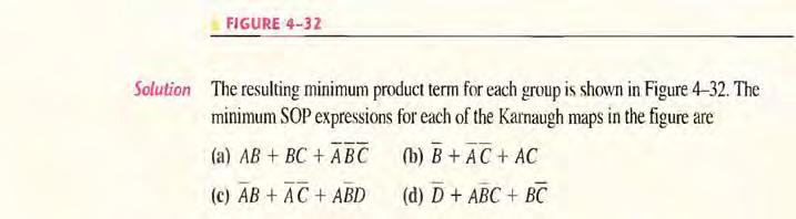
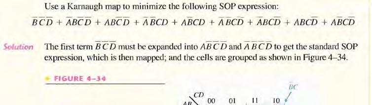
8 Example: Example: ٣٩


9 KARNAUGH MAP POS MINIMIZATION Karnaugh Map Simplification of POS Expressions The process for minimizing a POS expression is the same as for an SOP expression except that you group 0s to produce minimum sum terms instead of grouping 1s to produce minimum product terms. Example ٤٠


10 Converting Between POS and SOP Using the Karnaugh Map Don t care Karnough condition ٤١
, it results in an AND- OR-Invert circuit.")
11 Chapter 4 COMBINATIONAL LOGIC CIRCUITS AND-OR Logic AND-OR circuit consisting of two (2-input) AND gates and one 2-input OR gate; AND-OR-Invert Logic When the output of an AND-OR circuit is complemented (inverted), it results in an AND- OR-Invert circuit. Exclusive-OR logic we can used AND-OR to represent X-OR Exclusive-NOR Logic ٤٢

12 Example Example ٤٣

13 THE UNIVERSAL PROPERTY OF NAND AND NOR GATES The NAND Gate as a Universal Logic Element The NAND gate is a universal gate because it can be used to produce the NOT, the AND, the OR, and the NOR functions. An inverter can be made from a NAND gate by connecting all of the inputs together and creating, in effect, a single input, ٤٤

14 The NOR Gate as a Universal Logic Element Like the NAND gate, the NOR gate can be used to produce the NOT, AND. OR and NAND functions. As shown below: COMBINATIONAL LOGIC USING NAND AND NOR GATES NAND Logic NAND gate can function as either a NAND or a negative-or because, by DeMorgan"s theorem, ٤٥

15 Example: Example: Solution: ٤٦


16 NOR Logic A NOR gate can function as either a NOR or a negative-and, as shown by DeMorgan's theorem. Example ٤٧


17 CHAPYER FIVE BASIC ADDERS The Half-Adder The half-adder accepts two binary digits on its inputs and produces two binary digits on its outputs, a sum bit and a carry bit. Truth table for half adder From the operation of the halfadder as stated in Table The carry output expression Notice that the output Carry (C out ) is a 1 only when both A and B are 1 s: therefore. (C out ) can be expressed as the AND of the input variables. Half-adder logic diagram. ٤٨


18 The Full-Adder The full-adder accepts two input bits and an input carry and generates a sum output and an output carry. Full-Adder Logic Full-Adder Logic The full-adder must add the two input bits and the input carry from the half-adder. ٤٩


19 There are two half-adders, connected as shown in the block diagram with their output carries ORed. Example: ٥٠

 because there is no carry input to the least significant bit")
20 PARALLEL BINARY ADDERS Two or more full-adders have connected to form parallel binary adders. To add two binary numbers, a full-adder is required for each bit in the numbers. So for 2-bit numbers, two adders are needed; for 4-bit numbers, four adders are used; and so on. The carry output of each adder is connected to the carry input of the next higherorder adder, as shown in Figure below for a 2-bit adder. Notice that either a half-adder can be used for the least significant position or the carry input of a full-adder can be made 0 (grounded) because there is no carry input to the least significant bit position. In Figure above the least significant bits (LSB) of the two numbers are represented by A 1 and B1. The next higher-order bits are represented by A 2 and B 2. The three sum bits are 1, 2 and ٣ ' Notice that the output carry from the left-most full-adder becomes the most significant bit (MSB) in the sum, 3. Example ٥١


21 Four-Bit Parallel Adders A group of four bits is called a nibble. A basic 4-bit parallel adder is implemented with four full-adder stages as shown in Figure Truth Table for a 4-Bit Parallel Adder Table 6-3 is the truth table for a 4-bit adder. On some data sheets, truth tables may be called function tables or functional truth tables. The subscript n represents the adder bit and can be 1, 2, 3, or 4 for the 4-bit adder. C n-1 is the carry from the previous adder. Carries C 1, C 2 and C 3 are generated internally. C n is an external carry input and C 4 is an output. Example: ٥٢
, and if")
 The truth table and")


22 Half Subtractor A subtracted from B the output is Di (Difference), and if B greater than A we need to borrow and labeled (B o ) The truth table and block diagram of half subtractor as shown below Logic Diagram half subtractor. The Boolean expression for half subtractor D i = B o =. B Full subtractor Full subtractor we have Barrow in (B in ) the truth table as shown below Block symbol ٥٣


.")
23 We can construct full subtractor by using half subtractor as shown below Logic diagram as shown 4 bit parallel subtractor: the form bellow 4 bit parallel subtractor that can be subtract binary number B 3 B 2 B 1 B 0 from binary number A 3 A 2 A 1 A 0, Notice that the top subtractor (half subtractor ) subtract the LSBs(1s place). The B o of the 1s subtractor is tied to next subtractor as B in ٥٤
24 ٥٥
25 COMPARATORS The basic function of a comparator is to compare the magnitudes of two binary quantities to determine the relationship of those quantities. Equality Exclusive-OR gate can be used as a basic comparator because its output is a 1 if the two input bits are not equal and a 0 if the input bits are equal. In order to compare binary numbers containing two bits each, an additional exclusive OR gate is necessary. The two least significant bits (LSBs) of the two numbers are compared by gate G 1. In addition, the two most significant bits (MSBs) are compared by gate G 2, as shown in Figure below. If the two numbers are equal, their corresponding bits are the same, and the output of each exclusive-or gate is a 0. If the corresponding sets of bits are not equal. a 1 occurs on that exclusive-or gate output. In order to produce a single output indicating an equality or inequality of two numbers, two inverters and an AND gate can be used, ٥٦


 and an")
, as shown in the logic symbol for")
26 Example: Inequality In addition to the equality output, many IC comparators provide additional outputs that indicate which of the two binary numbers being compared is the larger. That is, there is an output that indicates when number A is greater than number B (A > B) and an output that indicates when number A is less than number B (A < B), as shown in the logic symbol for a 4-bit comparator.. Example: ٥٧


27 CODE CONVERTERS BCD-to-Binary Conversion One method of BCD-to-binary code conversion uses adder circuits. The basic conversion process is as follows: 1. The value, or weight, of each bit in the BCD number have represented by a binary number. 2. All of the binary representations of the weights of bits that are 1 s in the BCD number have added. 3. The result of this addition is the binary equivalent of the BCD number. The binary numbers representing the weights of the BCD bits have summed to produce the total binary number. Example: ٥٨

28 Binary-to-Gray and Gray-to-Binary Conversion Figure bellow shows a 4-bit binary-to-gray code converter. In addition, Figure bellow illustrates a 4-bit Gray-to-binary converter. Example: ٥٩

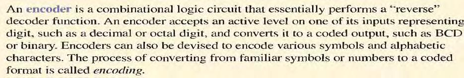
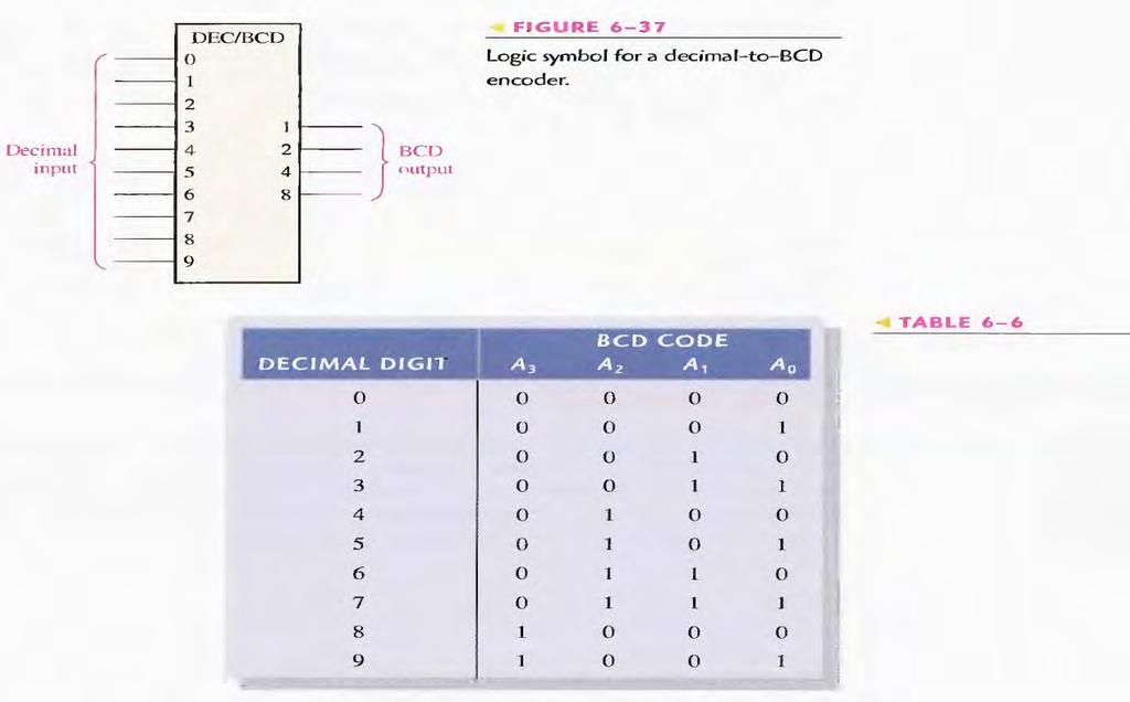
29 ENCODER ٦٠

 is applied to the data-select lines, the data on input D 0 appear on the data-output line.")
 is applied, the data on D 2 appear on the output.")
30 MULTIPLEXERS (DATA SELECTORS) Logic symbol for a 4-input multiplexer (MUX) is shown in Figure bellow. Notice that there are two data-select lines because with two select bits. Any one of the four data input lines have selected. 2-bit code on the data-select (S) inputs will allow the data on the selected data input to pass through to the data output. If a binary 0 (S 1 = 0 and So = 0) is applied to the data-select lines, the data on input D 0 appear on the data-output line. If a binary 1 (S 1 = 0 and S 0 = 1) is applied to the data-select lines, the data on input D 1 appear on the data output. If a binary 2 (S 1 = 1 and So = 0) is applied, the data on D 2 appear on the output. If a binary 3 (S 1 = 1 and So = 1) is applied, the data on D 3 When these terms are OR, the total expression for the data output is The implementation of this equation requires four 3-input AND gates, a 4-input OR gate, and two inverters to generate the complements of S 1 and S 2 ٦١
31 DEMULTIPLEXERS A demultiplexer (DEMUX), basically reverses the multiplexing function. It takes digital information from one line and distributes it to a given number of output lines. For this reason, the demultiplexer has known as a data distributor. In Figure shows a l-line-to-4-line demultiplexer (DEMUX) circuit. The data-input line goes to all of the AND gates. The two data-select lines enable only one gate at a time, and the data appearing on the data-input line will pass through the selected gate to the associated data-output line. ٦٢
 latch is formed with two cross-coupled NOR gates, as shown in Figure")

32 CHAPTER SIX/ Flip Flop The S-R (SET-RESET) Latch An active-high input S-R (SET-RESET) latch is formed with two cross-coupled NOR gates, as shown in Figure An active-low input latch has formed with two cross-coupled NAND gates, as shown in figure We start explain the operation by using Negative OR gates as shown in figure ٦٣


 the output are labeled Q and Q the D")
 at input D is delayed one clock")

33 The truth table as shown in figure below Logic symbols for both the active-high input and the active-low input latches are shown in figure D Flip Flop: Logic symbol for D- flip-flop has shown in figure It has only one data input (D) and clock input (CLK) the output are labeled Q and Q the D flipflop is often called delay flip flop because the data (0 or 1) at input D is delayed one clock pulse from getting to the output Q From truth table Notice that output Q fallows input D after one clock pulse (Q n+1 ) ٦٤
 and CLR (clear) ] PS input sets o/p Q=1 when enabled by logic 0 The CLR i/p clear o/p to 0 when enabled")

34 We can make D flip flop from a clocked R-S flip flop by adding inverter as shown Logic diagram of D flip flop As shown below Always we use the D flip flop contained in IC as shown in figure We have two extra input [PS(preset) and CLR (clear) ] PS input sets o/p Q=1 when enabled by logic 0 The CLR i/p clear o/p to 0 when enabled by logic 0 The PS and CLR override the D and CLK I/P As shown in truth table When we have the PS and CLR the flip flop operate as Asynchronous (not synchronous) If the flip flop disable the PS and CLR therefore in synchronous operation and can be set and reset by D and CLK input this can be see from the last two line in truth table. ٦٥


 and the synchronous")
35 J-K Flip Flop Most widely used and universal Flip Flop The I/P label J and K are data input CLK is the clock input Q and Q are the normal and complementary o/p From truth table we see If J and K =0 the flip flop in hold mode the data input not effect on output then the output in hold on last data present line 1 in truth table Line 2 and 3 is the reset and set condition for Q output Line 4 toggle position of J-K flip flop when both data J=K=1 therefore the Q O/P will repeat clock pulses causes turn off-on-off-on and so on The logic diagram of J-K flip-flop as shown The commercial logic symbols for J_K flip flop as shown We see asynchronous input (preset and clear) and the synchronous is the clock input ٦٦
36 Logic design Ibn Al Haitham collage /Computer science Eng. Sameer T Flip Flop The logic symbols for T- flip flop T Q CLK Q The output is toggle if the input data T =1 with clock (reverse of previous state) as shown in truth table Output Also can be used the J-K flip flop to represent T flip flop by short J and K = 1 ٦٧


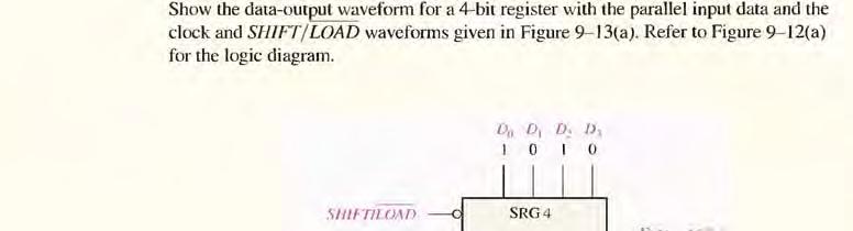
37 CHAPTER SEVEN SHIFT REGISTER BASIC SHIFT REGISTER FUNCTIONS A register is a digital circuit with two basic functions: data storage and data movement. We have many type of shift register as shown Serial IN/Serial OUT SHIFT REGISTERS The serial in/serial out shift register accepts data serially-that is, one bit at a time on a single line. It produces the stored information on its output also in serial form. Let first look at the serial entry of data into a typical shift register. Figure below shows a 4-bit device implemented with D flip-flops. With four stages, this register can store up to four bits of data. ٦٨

38 Example: ٦٩


39 SERIAL IN/PARALLEL OUT SHIFT REGISTERS in the parallel output register. the output of each stage is available. Once the data are stored, each bit appears on its respective output line, and all bits are available simultaneously, rather than on a bit-by-bit basis as with the serial Figure below shows a 4-bit serial in/parallel out shift register and its logic block symbol Example : PARALLEL IN/SERIAL OUT SHIFT REGISTERS For parallel data, multiple bits have transferred at one time. Figure below illustrates a 4-bit parallel in/serial out shift register and a typical logic symbol. Notice that there are four data-input lines, D 0, D 1, D 2, and D 3,and SHIFT / LOADinput, which allows four bits of data to load in parallel into the register. When SHIFT/ LOAD is LOW, gates G 1 through G 4 are enabled, allowing each data bit to be applied to the D input of its respective flip-flop. When a clock pulse is applied, the flip-flops with D = 1will set and those with D = 0 will reset. Thereby storing all four bits simultaneously. When SHIFT/ LOADis HIGH, gates G 1, through G 4 are disabled and gates G5; through G7 are enabled, allowing the data bits to shift right from one stage to the next. The OR gates allow either the normal shifting operation or the parallel data-entry operation, depending on which AND gates are enabled by the level on the SHIFT/ LOAD input. Notice that FF0 has a single AND to disable the parallel input, D 0. It does not require an AND/OR arrangement because there is no serial data in. ٧٠

40 Example ٧١

41 PARALLEL IN/PARALLEL OUT SHIFT REGISTERS The parallel in/parallel out register, immediately following the simultaneous entry of all data bits, the bits appear on the parallel outputs. ٧٢
 within the counter do not change states at exactly the same time because they do not have a common clock pulse.")
 has applied to the clock input (C) of only the first flop-flop, FF0, which is always the least significant bit (LSB).")
42 CHAPTER EIGHT Counters ASYNCHRONOUS COUNTER OPERATION The term asynchronous refers to events that do not have a fixed time relationship with each other and, generally, do not occur at the same time. An asynchronous counter is one in which the flip-flops (FF) within the counter do not change states at exactly the same time because they do not have a common clock pulse. A counter can have 2 n states, where n is the number of flip-flops. A 2-Bit Asynchronous Binary Counter Figure below shows a 2-bit counter connected for asynchronous operation. Notice that the clock (CLK) has applied to the clock input (C) of only the first flop-flop, FF0, which is always the least significant bit (LSB). The second flip-flop, FF1, is triggered by the Q 0 out put of FF0. FFO changes state at the positive-going edge of each clock pulse. But FF1 changes only when triggered by a positive-going transition of the Q 0 output of FF0. The binary state sequence of 2 bit as shown in table below Since it goes through a binary sequence, the counter in Figure 8-1 is a binary counter. It actually counts the number of clock pulses up to three, and on the fourth pulse it recycles to its original state (Q 0 = 0, Q 1 = 0). The term recycle has commonly applied to counter operation; it refers to the transition of the counter from its final state back to its original state. ٧٣
![The Timing Diagram The positive-going edge of CLKI (clock pulse]) causes the Q 0 output of FF0 to go HIGH, At the same time the Q 0 output goes low.](/docs-images/95/125537716/images/43-1.jpg "But it has no effect on FF1 because a positive -going transition must occur to trigger the flip-flop.")

43 The Timing Diagram The positive-going edge of CLKI (clock pulse]) causes the Q 0 output of FF0 to go HIGH, At the same time the Q 0 output goes low. But it has no effect on FF1 because a positive -going transition must occur to trigger the flip-flop. After the A 3-Bit Asynchronous Binary Counter The state sequence for a 3-bit binary counter has listed in table below: basic operation is the same as that of the 2-bit counter except that the 3- bit counter has eight states, due to its three flip-flops. Notice that the counter progresses through a binary count of zero through seven and then recycles to the zero state. This counter can be easily expanded for higher count, by connecting additional toggle flip-flops. ٧٤
 through nine (1001) is a BCD decade counter because its ten-state sequence produces the BCD code.")
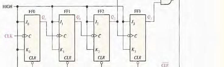
44 Asynchronous Decade Counters One common modulus for counters with truncated sequences is ten (called MOD10). Counters with ten states in their sequence have called decade counters. A decade counter with a count sequence of zero (0000) through nine (1001) is a BCD decade counter because its ten-state sequence produces the BCD code. To obtain a truncated sequence, it is necessary to force the counter to recycle before going through all of its possible states. For example, the BCD decade counter must recycle back to the 0000 state after the 100l state. One way to make the counter recycle after the count of nine (1001) is to decode count ten (l010) with a NAND gate and connect the output of the NAND gate to the clear ( CLR ) inputs of the flip-flops, as shown ٧٥


45 Example: ٧٦

46 SYNCHRONOUS COUNTER OPERATION The term synchronous refers to events that have a fixed time relationship with each other. A synchronous counter is one in which all the flip-flops in the counter have clocked at the same time by a common clock pulse. A 2-Bit Synchronous Binary Counter Figure below shows a 2-bit synchronous binary counter. Notice that an arrangement different from that for the asynchronous counter must be used for the J 1 and K 1 inputs of FF1 in order to achieve a binary sequence. The operation of this synchronous counter is as follows: First, assume that the counter is initially in the binary 0 state: that is. Both flip-flops are RESET. When the positive edge of the first clock pulse is applied, FF0 will toggle and Q 0 will therefore go HIGH. After CLK1, Q 0 = 1and Q 1 = 0. When the leading edge of CLK2 occurs, FF0 will toggle and Q 0 will go LOW. Since FF1 has a HIGH (Q 0 = 1) on its J1, and KI inputs at the triggering edge of this clock pulse, the flip-flop toggles and Q 1 goes HIGH. Thus, after CLK2, Q 0 = 0 and Q 1 = 1(which is a binary 2 state). When the leading edge of CLK3 occurs. FF0 again toggles to the SET state (Q 0 = 1), and FF1 remains SET (Q 1 =1) because its J 1 and K 1 inputs are both LOW (Q 0 = 0). After this triggering edge, Q 0 = 1 and Q 1 = 1 (which is a binary 3 state). Finally, at the leading edge of CLK4, Q 0 and Q 1 go LOW because they both have a toggle condition on their J and K inputs. ٧٧


47 A 3-Bit Synchronous Binary Counter A 3-bit synchronous binary counter is shown in Figure below its timing diagram is shown in Figure You can understand this counter operation by examining its sequence of states as shown in table First, let's look at Q 0. Notice that Q 0 changes on each clock pulse as the counter progresses from its original state to its final state and then back to its original state. To produce this operation, FF0 must be held in the toggle mode by constant HIGH on its J 0 and K 0 inputs. Notice that Q 1 goes to the opposite state following each time Q 0 is a 1. This change occurs at CLK2, CLK4, CLK6, and CLK8. The CLK8 pulse causes the counter to recycle. To produce this operation, Q 0 is connected to the J 1 and K 1 inputs of FF1. When Q 0 is a 1 and a clock pulse occurs, FF1 is in the toggle mode and therefore changes state. The other times, when Q 0 is a 0, FF1 is in the no-change mode and remains in its present state. Next, let's see how FF2 is made to change at the proper times according to the binary sequence. Notice that both times Q 2 changes state. it is preceded by the unique condition in which both Q 0 and Q 1 are HIGH. This condition is detected by the AND gate and applied to the J 2 and K 2 inputs of FF2. Whenever both Q 0 and Q 1 are HIGH, the output of the AND gate makes the J 2 and K 2 inputs of FF2 HIGH, and FF2 toggles on the following clock pulse. At all other times, the J 2 and K 2 inputs of FF2 are held LOW by the AND gate output, andff2 does not change state. ٧٨

 toggles on each clock pulse, so the logic equation for its J 0 and K 0 inputs is J 0 =K 0 =1 This equation is implemented by connecting J 0 and K 0 to a constant HIGH")
48 A 4-Bit Synchronous Binary Counter Figure below shows a 4-bit synchronous binary counter, This particular counter is implemented with negative edge-triggered flip- A 4-Bit Synchronous Decade Counter As you know, a BCD decade counter exhibits a truncated binary sequence and goes from 0000 through the 1001 state. Rather than going from the 1001 state to the 1010 state, it recycles to the 0000 state. A synchronous BCD decade counter is shown in Figure below. First, notice that FF0 (Q 0 ) toggles on each clock pulse, so the logic equation for its J 0 and K 0 inputs is J 0 =K 0 =1 This equation is implemented by connecting J 0 and K 0 to a constant HIGH level. Next, notice in Table below that FF1 (Q 1 ) changes on the next clock pulse each time Q 0 = 1 and Q 3 = 0, so the logic equation for the J 1 and K 1 inputs is ٧٩


49 FF3 as shown in the logic diagram States of a BCD decade counter.table UP/DOWN SYNCHRONOUS COUNTERS In general, most up/down counters can be reversed at any point in their sequence. Table below shows the complete up/down sequence for a 3-bit binary counter. The arrows indicate the state-to-state movement of the counter for both its UP and its DOWN modes of operation. An examination of Q 0 for both the up and down sequences shows that FF0 toggles on each clock pulse. Thus, the J 0 and K 0 inputs of FF0 are J 0 =K 0 =1 ٨٠


50 Figures below shows the logic diagram and truth table for UP/DOWN counter ٨١

51 CHAPTER NINE /Memories The Basic Semiconductor Memory Array Each storage element in a memory can retain either a I or a 0 and is called a cell. Memories made up of arrays of cells, as illustrated in Figure below Each block in the memory array represents one storage cell. and its location can be identified by specifying a row and a column. The location of a unit of data in a memory array called its address. The address of a byte specified only by the row. Basic Memory Operations Since a memory stores binary data. data must be put into the memory and data must be copied from the memory when needed. The write operation puts data into a specified address in the memory, and the read operation copies data out of a specified address in the memory. The addressing operation, which is part of both the write and the read operations, selects the specified memory address. Data units go into the memory during a write operation and come out of the memory during a read operation on a set of lines called the data bus. bus. As indicated in Figure below the data bus is bidirectional, which means that data can go in either direction (into the memory or out of the memory). ٨٢


52 In this case, of byte-organized memories, the data bus has at least eight lines so that all eight bits in a selected address are transferred in parallel. For write or read operation. An address selected by placing a binary code representing the desired address on a set of lines called the address bus. The address code is decoded internally. And the appropriate address is selected. The Write Operation A simplified write operation illustrated in Figure ٨٣


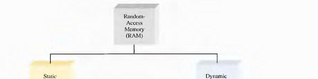
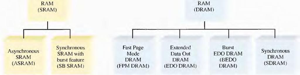
53 Read Operation A simplified read operation is illustrated in Figure Bit: The smallest unit of binary data Byte: data are handled in an 8-bit unit or in multiples of 8-bit units. Nibbles: The byte can be split into two 4-bit units Word: generally consists of one or more bytes. RANDOM-ACCESS MEMORIES (RAMs) RAM are read/write memories in which data can be written into or read from any selected address in any sequence. When a data unit is written into a given address in the RAM, the data unit previously stored at that address is replaced by the new data unit. When a data unit is read from a given address in the RAM, the data unit remains stored and is not erased by the read operation. This nondestructive read operation can be viewed as copying the content of an address while leaving the content intact. A RAM is typically used for short-term data storage because it cannot retain stored data when power is turned off. The RAM Family The two categories of RAM are the static RAM (SRAM) and the dynamic RAM (DRAM). Static RAMs generally use latches as storage elements and can therefore store data indefinitely as long as dc power is applied. Dynamic RAMs use capacitors as storage elements and cannot retain data very long without the capacitors being recharged by a process called refreshing. Data can be read much faster from SRAMs than from DRAMs. DRAMs can store much more data than SRAMs for a given physical size and cost because the DRAM cell is much simpler, and more cells can be crammed into a given chip area than in the SRAM. The type of RAM as shown in figure below ٨٤
54 ٨٥

55 READ-ONLY MEMORIES (ROMs) ROM contain permanently or semi permanently stored data, Which can be read from the memory but either cannot be changed at all or cannot be changed without specialized equipment. ROMs retain stored data when the power is off and are therefore nonvolatile memories. The mask ROM is the type in which the data are permanently stored in the memory during the manufacturing process. The PROM, or programmable ROM, is the type in which the data are electrically stored by the user with the aid of specialized equipment. The EPROM, or erasable PROM. The UV EPROM is electrically programmable by the user, but the stored data must be erased by exposure to ultraviolet light over a period of several minutes. The electricallyerasable PROM (EEPROM or E 2 PROM) can be erased in a few milliseconds. The types of ROM as shown in figure below ٨٦

56 2011 first class 1- Number system and codes Chapter one The binary number system and digital codes are fundamental to computers and to digital electronics in general. The binary number system and its relationship to other number systems such as decimal, hexadecimal, and octal has presented. Arithmetic operations with binary numbers have covered to provide a basis for understanding how computers and many other types of digital systems work. 1.1 DECIMAL NUMBERS We are familiar with the decimal number system because we use decimal numbers every day. The decimal number system has ten digits, 0 through 9. Represent a certain Therefore, these digits not limited because used in different position. As shown in example below. For example The position of each digit in a decimal number indicates the magnitude of the quantity represented and could assign a weight. The weights for whole numbers are positive powers of ten that increase from right to left, beginning with 10 0 = 1. For fractional numbers, the weights are negative powers of ten that decrease from left to right beginning with Example: 1

57 2011 first class 1.2 BINARY NUMBERS The binary number has only two digits (bits) 1 and 0. The position of a 1 or 0 in a binary number indicates its weight or value within the number, The weights in a binary number have based on power of two. As we have seen in Table above, four bits are required to count from zero to 15. In general, with n bits we can count to a number equal to 2 n -1 Largest decimal number count = 2 n -1 With six bits (n = 4) you can count from zero to sixty-three = 16-1 = 15 A binary number is a weighted number. The right most bit is the LSB (least significant bit) in a binary whole number and has a weight of 2 0 = 1. The weights increase from right to left by a power of two for each bit. The left most bit is the MSB (most significant bit). Frictional numbers can be represents in binary by placing bits to the right of the binary point. The left most bit is the MSB in a binary fractional number, the fractional weights decrease from left to right by a negative power of two for each bit. Figure below show the weights of binary fraction number where n is the number of bits from the binary point. 2


58 2011 first class Binary weight table as shown below 1.3 OCTAL NUMBERS The octal number system is composed of eight digits, which are 0, 1, 2, 3, 4, 5, 6, 7 Each octal number can be represented by three digits only 000 to HEXADECIMAL NUMBERS The hexadecimal number system consists of digits 0 9 and le ers A F. 3


59 2011 first class Decimal to binary conversion. We have two method discussed below Conversion between systems 1. Sum of Weights Method One way to find the binary number that is equivalent to a given decimal number is to determine the set of binary weights whose sum is equal to the decimal number. Example: 2. Repeated Division by 2 Method To get the binary number for a given decimal number, divide the decimal number by 2 un l the quotient is zero. Remainders form is the binary number. Examples below explain the process for more detail. Examples : 4
60 2011 first class Converting Decimal Fractions to Binary An easy way to remember frac onal binary weights is that the most significant weight is 0.5, which is 2 1 and that by halving any weight, you get the next lower weight; thus a list of four frac onal binary weights would be 0.5, 0.25, 0.125, Sum of Weights The sum of weights method could apply to fractional decimal numbers, we determine the fraction binary wait whose sum equal to decimal number as shown in the following example: Example: 2. Repeated Mul plica on by 2 As you have seen, decimal whole numbers can be converted to binary by repeated division by 2. Decimal frac ons can be converted to binary by repeated mul plica on by 2, the carry digits are the binary number we stop multiplication when the fraction part of multiplication equal to zero For example, 5


61 2011 first class Binary to Decimal Conversion The decimal value of any binary number can be founds by adding the weights of all bits that are 1 and discarding the weights of all bits that are zero. Examples below more detail to conversion. Example1: Example2: Decimal to Octal Conversion : A method of converting a decimal number to an octal number is the repeated division by 8 Example Octal to Decimal Conversion The evaluation of an octal number in terms of its decimal equivalent has accomplished by multiplying each digit by its weight and summing the products. 6


62 2011 first class Decimal to Hexadecimal Conversion Repeated division of a decimal number by 16 will produce the equivalent hexadecimal number, formed by the remainders of the divisions. The first remainder produced is the least significant digit (LSD). Each successive division by 16 yields a remainder that becomes digit in the equivalent hexadecimal number. Note that when a quotient has a fractional part, the fractional part has multiplied by the divisor to get the remainder. Hexadecimal to Decimal Conversion One way to find the decimal equivalent of a hexadecimal number is to first convert the hexadecimal number to binary and then convert from binary to decimal. Another way to convert a hexadecimal number to its decimal equivalent is to multiply The decimal value of each hexadecimal digit by its weight and then take the sum of these products, the weights of a hexadecimal number are increasing powers of 16 (from right to le ). For a 4 digit hexadecimal number, the weights are 7


63 2011 first class Example: Binary to Octal Conversion of a binary number to an octal number is the reverse of the octal to binary conversion Example Octal to Binary Conversion : Because each octal digit can be represented by a 3 bit binary number, Example: 8


64 2011 first class Binary to Hexadecimal Conversion Converting a binary number to hexadecimal is a straightforward procedure. Simply break the binary number into 4 bit groups. Starting at the right most bit, replace each 4 bit group with the equivalent hexadecimal symbol. Hexadecimal to Binary Conversion To convert from a hexadecimal number to a binary number, reverse the process and replace each hexadecimal symbol with the appropriate four bits. Example: Octal to Hexadecimal Conversion To convert the octal to hex number by the fallowing steps 1 Convert the octal number to binary 2 Make group 4 digit and we add 0 to MSB 3 Convert the number to Hex Example: convert to Hexadecimal number Octal Binary 00 ( ) HEX (1 E C) 16 9
65 2011 first class Hexadecimal to Octal Conversion To convert the hex number to octal by 1 Convert the Hex number to binary 2 Make group for 3 digit and add 0 to MSB 3 Convert the number to octal Example: convert the Hex (FD4) 16 to octal (F D 4) ( ) ( ) ( ) 8 10


66 2011 first class BINARY ARITHMETIC Binary Addition The four basic rules for adding binary digits (bits) are as follows: When there is a carry of 1, you have a situa on in which three bits are being added (bit in each of the two numbers and a carry bit). This situation has illustrated as follows: Example: Addition in octal When we add two octal number if greater than 7 we subtract 8 from result digit Example: = 8 >7 than 8 8=0 with carry =12 >7 than 12 8 = 4 with carry 1 11


67 2011 first class Hexadecimal Addition : use the following rules: Example: 12

 + 1 An alternative method of finding the 2's complement of a binary number is as follows: 1.")
68 2011 first class : COMPLEMENTS: 1'S AND 2'S COMPLEMENTS OF BINARY NUMBERS The l's complement and the 2's complement of a binary number are important because they permit the representa on of nega ve numbers. The method of 2's complement arithmetic has commonly used in computers to handle negative numbers. Finding the 1's Complement The 1's complement of a binary number were found by changing all 1s to 0s and all 0s to 1s, As illustrated: The 2' s Complement Example: 2's complement = (1's complement) + 1 An alternative method of finding the 2's complement of a binary number is as follows: 1. Start at the right with the LSB and write the bits as they are up to and including the first Take the 1's complements of the remaining bits. 13


69 2011 first class 1 st And 2 nd complement in decimal 1 st And 2 nd complement in hexadecimal number 14


70 2011 first class Method three : 15


71 2011 first class Binary Subtraction Subtraction is addition with the sign of the subtrahend changed, and adds it to the minuend. The result of a subtraction has called the difference. To subtract two signed numbers, take the 2's complement of the subtrahend and add. Discard any final carry bit. Example: 16

 form.")

72 2011 first class Multiplication The sign of the product of a multiplication depends on the signs of the multiplicand and the multiplier according to the following two rules: If the signs are the same, the product is positive. If the signs are different, the product is negative. The basic steps in the partial products method of binary multiplication are as follows: Step 1. Determine if the signs of the mul plicand and mul plier are the same or different. This determines what the sign of the product will be. Step 2. Change any negative number to true (uncomplemented) form. Because most computers store nega ve numbers in 2's complement, a 2's complement opera on is required to get the negative number into true form. Step 3. Star ng with the least significant mul plier bit, generate the partial products. When the mul plier bit is 1, the par al product is the same as the mul plicand. When the mul plier bit is 0, the par al product is zero. Shi each successive par al product one bit to the left. Step 4. Add each successive par al product to the sum of the previous par al products to get the final product. Step 5. if the sign bit that was determined in step 1 is nega ve. Take the 2's complement of the product. if positive. Leave the product in true form. Attach the sign bit to the product. Example 17
 form.")
73 2011 first class Division The sign of the quotient depends on the signs of the dividend and the divisor according to the following two rules: If the signs are the same, the quotient is positive. If the signs are different, the quotient is negative. When two binary numbers are divided, both numbers must be in true (uncomplememed) form. The basic steps in a division process are as follows: Step 1. Determine if the signs of the dividend and divisor are the same or different. This determines what the sign of the quotient will be. Initialize the quotient to zero. Step 2. Subtract the divisor from the dividend using 2's complement addi on to get the first par al remainder and add 1 to the quo ent. If this par al remainder is posi ve, go to step 3. If the par al remainder is zero or nega ve, the division is complete. Step 3. Subtract the divisor from the par al remainder and add 1 to the quo ent. If the result is positive, repeat for the next partial remainder. If the result is zero or negative, the division is complete. Example 18

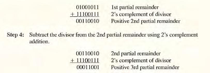
74 2011 first class 19


75 2011 first class Chapter two BINARY CODED DECIMAL (BCD) : The 8421 code is a type of BCD (binary coded decimal) code. Binary coded decimal means that each decimal digit, 0 through 9, is represented by a binary code of four bits. Example: BCD Addition Step 1. Add the two BCD numbers, using the rules for binary addition. Step 2. If a 4 bit sum is equal to or less than 9, it is a valid BCD number. Step 3. If a 4 bit sum is greater than 9, or if a carry out of the 4 bit group is generated, it is an invalid result. Add 6 (0110) to the 4 bit sum in order to skip the six invalid states and return the code to If a carry results when 6 is added. simply add the carry to the next 4 bit group. Examples 20


76 Logic design Ibn Al Haitham collage /Computer science Eng. Sameer 2011 first class Exess 3 21

77 2011 first class The Gray Code The Gray code is un weighted and is not an arithmetic code; that is, there are no specific weights assigned to the bit positions. Binary to Gray Code Conversion Gray to Binary Conversion 22


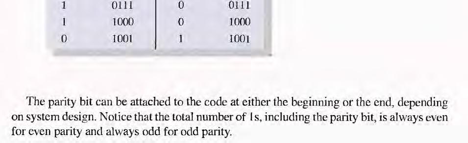
78 2011 first class Parity code 23


79 2011 first class Chapter three Boolean algebra INVERTER Standard logic symbols for the inverter are shown in Figure below: Inverter Truth Table When a HIGH level is applied to an inverter input, a LOW level will appear on its output. When a LOW level is applied to its input, a HIGH will appear on its output. logic Expression for an Inverter In Boolean algebra, which is the mathematics of logic circuits the operation of an inverter (NOT circuit) can be expressed as follows: If the input variable is called, A and the output variable is called X, then AND GATE An AND gate produces a HIGH output only when all of the inputs are HIGH, otherwise any of the inputs is LOW or both low, the output is LOW. 24


80 2011 first class AND Gate Truth Table The total number of possible combinations of binary inputs to a gate is determined by the following formula: N= 2 n The opera on of a 2 input AND gate can be expressed in equation form as follows: If one input variable is A, the other input variable is B, and the output variable is X, then the Boolean expression is X=A.B OR GATE An OR gate symbol as shown in figure OR Gate Truth Table For a 2 input OR gate, output X is HIGH when either input A or input B is HIGH, or when both A and B are HIGH; X is LOW only when both A and B are LOW. Logic Expressions for an OR Gate The logical OR function of two variables is represented mathematically by a (+) between the two variables, for example, A + B. 25

81 2011 first class NAND GATE The term NAND is a contraction of NOT AND and implies an AND function with a complemented (inverted) output. Operation of a NAND Gate For a 2 input NAND gate, output X is LOW only when inputs A and B are HIGH; X is HIGH when either A or B is LOW, or when both A and B are LOW. Logic Expressions for a NAND Gate 26

 gate is shown in Figure Output X is HIGH when input A is")
 gate are shown in Figure Output X is LOW when input A")
82 2011 first class NOR GATE The NOR is the same as the OR except the output is inverted. For a 2 input NOR gate, output X is LOW when either input A or input B is HIGH, or when both A and B are HIGH; X is HIGH only when both A and B are LOW. Exclusive OR Gate Standard symbols for an exclusive OR (XOR) gate is shown in Figure Output X is HIGH when input A is LOW and input B is HIGH, or when input A is HIGH and input B is LOW: X is LOW when A and B are both HIGH or both LOW. Exclusive NOR Gate Standard symbols for an exclusive NOR (XNOR) gate are shown in Figure Output X is LOW when input A is LOW and input B is HIGH, or when A is HIGH and B is LOW; X is HIGH when A and B are both HIGH or both LOW. 27

83 2011 first class LAWS AND RULES OF BOOLEAN ALGEBRA Laws of Boolean Algebra Equa on 1 Equa on 2 Equa on 3 Equa on 4 Equa on 5 28


84 2011 first class Rules of Boolean algebra Table below lists 12 basic rules that are useful in manipula ng and simplifying Boolean expressions. Rule 1. A + 0 = A : A variable OR with 0 is always equal to the variable. Rule 2. A + 1 = 1 : A variable OR with 1 is always equal to 1. Rule 3. A. 0 = 0 A variable AND with 0 is always equal to 0. Rule 4. A. 1 = A :A variable AND with 1 is always equal to the variable. Rule 5. A + A = A : A variable OR with itself is always equal to the variable. 29


85 2011 first class Rule 7. A. A = A: A variable AND with itself is always equal to the variable. 30
86 2011 first class 31
D I G I T A L C I R C U I T S E E
 D I G I T A L C I R C U I T S E E Digital Circuits Basic Scope and Introduction This book covers theory solved examples and previous year gate question for following topics: Number system, Boolean algebra,
II/IV B.Tech (Regular/Supplementary) DEGREE EXAMINATION. Answer ONE question from each unit.
 DEGREE EXAMINATION. Answer ONE question from each unit.") Hall Ticket Number: 14CS IT303 November, 2017 Third Semester Time: Three Hours Answer Question No.1 compulsorily. II/IV B.Tech (Regular/Supplementary) DEGREE EXAMINATION Common for CSE & IT Digital Logic
Hall Ticket Number: 14CS IT303 November, 2017 Third Semester Time: Three Hours Answer Question No.1 compulsorily. II/IV B.Tech (Regular/Supplementary) DEGREE EXAMINATION Common for CSE & IT Digital Logic
Injntu.com Injntu.com Injntu.com R16
 1. a) What are the three methods of obtaining the 2 s complement of a given binary (3M) number? b) What do you mean by K-map? Name it advantages and disadvantages. (3M) c) Distinguish between a half-adder
CONTENTS CHAPTER 1: NUMBER SYSTEM. Foreword...(vii) Preface... (ix) Acknowledgement... (xi) About the Author...(xxiii)
 Preface... (ix) Acknowledgement... (xi) About the Author...(xxiii)") CONTENTS Foreword...(vii) Preface... (ix) Acknowledgement... (xi) About the Author...(xxiii) CHAPTER 1: NUMBER SYSTEM 1.1 Digital Electronics... 1 1.1.1 Introduction... 1 1.1.2 Advantages of Digital Systems...
CONTENTS Foreword...(vii) Preface... (ix) Acknowledgement... (xi) About the Author...(xxiii) CHAPTER 1: NUMBER SYSTEM 1.1 Digital Electronics... 1 1.1.1 Introduction... 1 1.1.2 Advantages of Digital Systems...
MGU-BCA-205- Second Sem- Core VI- Fundamentals of Digital Systems- MCQ s. 2. Why the decimal number system is also called as positional number system?
 MGU-BCA-205- Second Sem- Core VI- Fundamentals of Digital Systems- MCQ s Unit-1 Number Systems 1. What does a decimal number represents? A. Quality B. Quantity C. Position D. None of the above 2. Why the
DIGITAL ELECTRONICS. Vayu Education of India
 DIGITAL ELECTRONICS ARUN RANA Assistant Professor Department of Electronics & Communication Engineering Doon Valley Institute of Engineering & Technology Karnal, Haryana (An ISO 9001:2008 ) Vayu Education
Principles of Digital Techniques PDT (17320) Assignment No State advantages of digital system over analog system.
 Assignment No State advantages of digital system over analog system.") Assignment No. 1 1. State advantages of digital system over analog system. 2. Convert following numbers a. (138.56) 10 = (?) 2 = (?) 8 = (?) 16 b. (1110011.011) 2 = (?) 10 = (?) 8 = (?) 16 c. (3004.06)
Assignment No. 1 1. State advantages of digital system over analog system. 2. Convert following numbers a. (138.56) 10 = (?) 2 = (?) 8 = (?) 16 b. (1110011.011) 2 = (?) 10 = (?) 8 = (?) 16 c. (3004.06)
SUBJECT CODE: IT T35 DIGITAL SYSTEM DESIGN YEAR / SEM : 2 / 3
 UNIT - I PART A (2 Marks) 1. Using Demorgan s theorem convert the following Boolean expression to an equivalent expression that has only OR and complement operations. Show the function can be implemented
VALLIAMMAI ENGINEERING COLLEGE. SRM Nagar, Kattankulathur DEPARTMENT OF ELECTRONICS AND COMMUNICATION ENGINEERING EC6302 DIGITAL ELECTRONICS
 VALLIAMMAI ENGINEERING COLLEGE SRM Nagar, Kattankulathur-603 203 DEPARTMENT OF ELECTRONICS AND COMMUNICATION ENGINEERING EC6302 DIGITAL ELECTRONICS YEAR / SEMESTER: II / III ACADEMIC YEAR: 2015-2016 (ODD
Computer Logical Organization Tutorial
 Computer Logical Organization Tutorial COMPUTER LOGICAL ORGANIZATION TUTORIAL Simply Easy Learning by tutorialspoint.com tutorialspoint.com i ABOUT THE TUTORIAL Computer Logical Organization Tutorial Computer
COLLEGE OF ENGINEERING DEPARTMENT OF ELECTRICAL AND ELECTRONICS ENGINEERING QUESTION BANK SUBJECT CODE & NAME: EC 1312 DIGITAL LOGIC CIRCUITS UNIT I
 KINGS COLLEGE OF ENGINEERING DEPARTMENT OF ELECTRICAL AND ELECTRONICS ENGINEERING QUESTION BANK SUBJECT CODE & NAME: EC 1312 DIGITAL LOGIC CIRCUITS YEAR / SEM: III / V UNIT I NUMBER SYSTEM & BOOLEAN ALGEBRA
DIGITAL ARITHMETIC: OPERATIONS AND CIRCUITS
 C H A P T E R 6 DIGITAL ARITHMETIC: OPERATIONS AND CIRCUITS OUTLINE 6- Binary Addition 6-2 Representing Signed Numbers 6-3 Addition in the 2 s- Complement System 6-4 Subtraction in the 2 s- Complement
BINARY SYSTEM. Binary system is used in digital systems because it is:
 CHAPTER 2 CHAPTER CONTENTS 2.1 Binary System 2.2 Binary Arithmetic Operation 2.3 Signed & Unsigned Numbers 2.4 Arithmetic Operations of Signed Numbers 2.5 Hexadecimal Number System 2.6 Octal Number System
MULTIMEDIA COLLEGE JALAN GURNEY KIRI KUALA LUMPUR
 STUDENT IDENTIFICATION NO MULTIMEDIA COLLEGE JALAN GURNEY KIRI 54100 KUALA LUMPUR SECOND SEMESTER FINAL EXAMINATION, 2013/2014 SESSION ITC2223 COMPUTER ORGANIZATION & ARCHITECTURE DSEW-E-F 1/13 18 FEBRUARY
UPY14602-DIGITAL ELECTRONICS AND MICROPROCESSORS Lesson Plan
 UPY14602-DIGITAL ELECTRONICS AND MICROPROCESSORS Lesson Plan UNIT I - NUMBER SYSTEMS AND LOGIC GATES Introduction to decimal- Binary- Octal- Hexadecimal number systems-inter conversions-bcd code- Excess
CHW 261: Logic Design
 CHW 261: Logic Design Instructors: Prof. Hala Zayed Dr. Ahmed Shalaby http://www.bu.edu.eg/staff/halazayed14 http://bu.edu.eg/staff/ahmedshalaby14# Slide 1 Slide 2 Slide 3 Digital Fundamentals CHAPTER
Chapter Three. Digital Components
 Chapter Three 3.1. Combinational Circuit A combinational circuit is a connected arrangement of logic gates with a set of inputs and outputs. The binary values of the outputs are a function of the binary
This tutorial gives a complete understanding on Computer Logical Organization starting from basic computer overview till its advanced architecture.
 About the Tutorial Computer Logical Organization refers to the level of abstraction above the digital logic level, but below the operating system level. At this level, the major components are functional
DIRECTORATE OF TECHNICAL EDUCATION DIPLOMA IN ELECTRICAL AND ELECTRONICS ENGINEERING II YEAR M SCHEME IV SEMESTER.
 DIRECTORATE OF TECHNICAL EDUCATION DIPLOMA IN ELECTRICAL AND ELECTRONICS ENGINEERING II YEAR M SCHEME IV SEMESTER 2015 2016 onwards DIGITAL ELECTRONICS CURRICULUM DEVELOPMENT CENTRE Curriculum Development
3. The high voltage level of a digital signal in positive logic is : a) 1 b) 0 c) either 1 or 0
 1 b) 0 c) either 1 or 0") 1. The number of level in a digital signal is: a) one b) two c) four d) ten 2. A pure sine wave is : a) a digital signal b) analog signal c) can be digital or analog signal d) neither digital nor analog
1. The number of level in a digital signal is: a) one b) two c) four d) ten 2. A pure sine wave is : a) a digital signal b) analog signal c) can be digital or analog signal d) neither digital nor analog
Code No: R Set No. 1
 Code No: R059210504 Set No. 1 II B.Tech I Semester Regular Examinations, November 2006 DIGITAL LOGIC DESIGN ( Common to Computer Science & Engineering, Information Technology and Computer Science & Systems
Philadelphia University Student Name: Student Number:
 Philadelphia University Student Name: Student Number: Faculty of Engineering Serial Number: Final Exam, First Semester: 2018/2019 Dept. of Computer Engineering Course Title: Logic Circuits Date: 03/01/2019
END-TERM EXAMINATION
 (Please Write your Exam Roll No. immediately) END-TERM EXAMINATION DECEMBER 2006 Exam. Roll No... Exam Series code: 100919DEC06200963 Paper Code: MCA-103 Subject: Digital Electronics Time: 3 Hours Maximum
IT 201 Digital System Design Module II Notes
 IT 201 Digital System Design Module II Notes BOOLEAN OPERATIONS AND EXPRESSIONS Variable, complement, and literal are terms used in Boolean algebra. A variable is a symbol used to represent a logical quantity.
Digital Fundamentals. CHAPTER 2 Number Systems, Operations, and Codes
 Digital Fundamentals CHAPTER 2 Number Systems, Operations, and Codes Decimal Numbers The decimal number system has ten digits: 0, 1, 2, 3, 4, 5, 6, 7, 8, and 9 The decimal numbering system has a base of
Scheme G. Sample Test Paper-I
 Sample Test Paper-I Marks : 25 Times:1 Hour 1. All questions are compulsory. 2. Illustrate your answers with neat sketches wherever necessary. 3. Figures to the right indicate full marks. 4. Assume suitable
COMBINATIONAL LOGIC CIRCUITS
 COMBINATIONAL LOGIC CIRCUITS 4.1 INTRODUCTION The digital system consists of two types of circuits, namely: (i) Combinational circuits and (ii) Sequential circuits A combinational circuit consists of logic
R07. Code No: V0423. II B. Tech II Semester, Supplementary Examinations, April
 SET - 1 II B. Tech II Semester, Supplementary Examinations, April - 2012 SWITCHING THEORY AND LOGIC DESIGN (Electronics and Communications Engineering) Time: 3 hours Max Marks: 80 Answer any FIVE Questions
1. Mark the correct statement(s)
") 1. Mark the correct statement(s) 1.1 A theorem in Boolean algebra: a) Can easily be proved by e.g. logic induction b) Is a logical statement that is assumed to be true, c) Can be contradicted by another
1. Mark the correct statement(s) 1.1 A theorem in Boolean algebra: a) Can easily be proved by e.g. logic induction b) Is a logical statement that is assumed to be true, c) Can be contradicted by another
B.Tech II Year I Semester (R13) Regular Examinations December 2014 DIGITAL LOGIC DESIGN
 Regular Examinations December 2014 DIGITAL LOGIC DESIGN") B.Tech II Year I Semester () Regular Examinations December 2014 (Common to IT and CSE) (a) If 1010 2 + 10 2 = X 10, then X is ----- Write the first 9 decimal digits in base 3. (c) What is meant by don
B.Tech II Year I Semester () Regular Examinations December 2014 (Common to IT and CSE) (a) If 1010 2 + 10 2 = X 10, then X is ----- Write the first 9 decimal digits in base 3. (c) What is meant by don
DE Solution Set QP Code : 00904
 DE Solution Set QP Code : 00904 1. Attempt any three of the following: 15 a. Define digital signal. (1M) With respect to digital signal explain the terms digits and bits.(2m) Also discuss active high and
DIGITAL SYSTEM DESIGN
 DIGITAL SYSTEM DESIGN UNIT I: Introduction to Number Systems and Boolean Algebra Digital and Analog Basic Concepts, Some history of Digital Systems-Introduction to number systems, Binary numbers, Number
R10. II B. Tech I Semester, Supplementary Examinations, May
 SET - 1 1. a) Convert the following decimal numbers into an equivalent binary numbers. i) 53.625 ii) 4097.188 iii) 167 iv) 0.4475 b) Add the following numbers using 2 s complement method. i) -48 and +31
Microcomputers. Outline. Number Systems and Digital Logic Review
 Microcomputers Number Systems and Digital Logic Review Lecture 1-1 Outline Number systems and formats Common number systems Base Conversion Integer representation Signed integer representation Binary coded
Digital logic fundamentals. Question Bank. Unit I
 Digital logic fundamentals Question Bank Subject Name : Digital Logic Fundamentals Subject code: CA102T Staff Name: R.Roseline Unit I 1. What is Number system? 2. Define binary logic. 3. Show how negative
VALLIAMMAI ENGINEERING COLLEGE
 VALLIAMMAI ENGINEERING COLLEGE SRM Nagar, Kattankulathur 603 203 DEPARTMENT OF INFORMATION TECHNOLOGY & COMPUTER SCIENCE AND ENGINEERING QUESTION BANK II SEMESTER CS6201- DIGITAL PRINCIPLE AND SYSTEM DESIGN
COPYRIGHTED MATERIAL INDEX
 INDEX Absorption law, 31, 38 Acyclic graph, 35 tree, 36 Addition operators, in VHDL (VHSIC hardware description language), 192 Algebraic division, 105 AND gate, 48 49 Antisymmetric, 34 Applicable input
Digital Fundamentals
 Digital Fundamentals Tenth Edition Floyd Chapter 2 2009 Pearson Education, Upper 2008 Pearson Saddle River, Education NJ 07458. All Rights Reserved Decimal Numbers The position of each digit in a weighted
INSTITUTE OF AERONAUTICAL ENGINEERING (Autonomous) Dundigal, Hyderabad
 Dundigal, Hyderabad") INSTITUTE OF AERONAUTICAL ENGINEERING (Autonomous) Dundigal, Hyderabad - 500 043 COMPUTER SCIENCE AND ENGINEERING TUTORIAL QUESTION BANK Name : DIGITAL LOGIC DESISN Code : AEC020 Class : B Tech III Semester
INSTITUTE OF AERONAUTICAL ENGINEERING (Autonomous) Dundigal, Hyderabad - 500 043 COMPUTER SCIENCE AND ENGINEERING TUTORIAL QUESTION BANK Name : DIGITAL LOGIC DESISN Code : AEC020 Class : B Tech III Semester
DHANALAKSHMI SRINIVASAN COLLEGE OF ENGINEERING AND TECHNOLOGY
 DHANALAKSHMI SRINIVASAN COLLEGE OF ENGINEERING AND TECHNOLOGY Dept/Sem: II CSE/03 DEPARTMENT OF ECE CS8351 DIGITAL PRINCIPLES AND SYSTEM DESIGN UNIT I BOOLEAN ALGEBRA AND LOGIC GATES PART A 1. How many
VALLIAMMAI ENGINEERING COLLEGE
 VALLIAMMAI ENGINEERING COLLEGE SRM Nagar, Kattankulathur 603 203 DEPARTMENT OF INFORMATION TECHNOLOGY QUESTION BANK Academic Year 2018 19 III SEMESTER CS8351-DIGITAL PRINCIPLES AND SYSTEM DESIGN Regulation
SECTION-A
 M.Sc(CS) ( First Semester) Examination,2013 Digital Electronics Paper: Fifth ------------------------------------------------------------------------------------- SECTION-A I) An electronics circuit/ device
R a) Simplify the logic functions from binary to seven segment display code converter (8M) b) Simplify the following using Tabular method
 Simplify the logic functions from binary to seven segment display code converter (8M) b) Simplify the following using Tabular method") SET - 1 1. a) Convert the decimal number 250.5 to base 3, base 4 b) Write and prove de-morgan laws c) Implement two input EX-OR gate from 2 to 1 multiplexer (3M) d) Write the demerits of PROM (3M) e) What
SET - 1 1. a) Convert the decimal number 250.5 to base 3, base 4 b) Write and prove de-morgan laws c) Implement two input EX-OR gate from 2 to 1 multiplexer (3M) d) Write the demerits of PROM (3M) e) What
Dec Hex Bin ORG ; ZERO. Introduction To Computing
 Dec Hex Bin 0 0 00000000 ORG ; ZERO Introduction To Computing OBJECTIVES this chapter enables the student to: Convert any number from base 2, base 10, or base 16 to any of the other two bases. Add and
Code No: R Set No. 1
 Code No: R059210504 Set No. 1 II B.Tech I Semester Supplementary Examinations, February 2007 DIGITAL LOGIC DESIGN ( Common to Computer Science & Engineering, Information Technology and Computer Science
DIGITAL SYSTEM FUNDAMENTALS (ECE 421) DIGITAL ELECTRONICS FUNDAMENTAL (ECE 422) COURSE / CODE NUMBER SYSTEM
 DIGITAL ELECTRONICS FUNDAMENTAL (ECE 422) COURSE / CODE NUMBER SYSTEM") COURSE / CODE DIGITAL SYSTEM FUNDAMENTALS (ECE 421) DIGITAL ELECTRONICS FUNDAMENTAL (ECE 422) NUMBER SYSTEM A considerable subset of digital systems deals with arithmetic operations. To understand the
COURSE / CODE DIGITAL SYSTEM FUNDAMENTALS (ECE 421) DIGITAL ELECTRONICS FUNDAMENTAL (ECE 422) NUMBER SYSTEM A considerable subset of digital systems deals with arithmetic operations. To understand the
(ii) Simplify and implement the following SOP function using NOR gates:
 Simplify and implement the following SOP function using NOR gates:") DHANALAKSHMI COLLEGE OF ENGINEERING DEPARTMENT OF ELECTRONICS AND COMMUNICATION ENGINEERING EE6301 DIGITAL LOGIC CIRCUITS UNIT I NUMBER SYSTEMS AND DIGITAL LOGIC FAMILIES PART A 1. How can an OR gate be
DHANALAKSHMI COLLEGE OF ENGINEERING DEPARTMENT OF ELECTRONICS AND COMMUNICATION ENGINEERING EE6301 DIGITAL LOGIC CIRCUITS UNIT I NUMBER SYSTEMS AND DIGITAL LOGIC FAMILIES PART A 1. How can an OR gate be
 www.vidyarthiplus.com Question Paper Code : 31298 B.E./B.Tech. DEGREE EXAMINATION, NOVEMBER/DECEMBER 2013. Third Semester Computer Science and Engineering CS 2202/CS 34/EC 1206 A/10144 CS 303/080230012--DIGITAL
SHRI ANGALAMMAN COLLEGE OF ENGINEERING. (An ISO 9001:2008 Certified Institution) SIRUGANOOR, TIRUCHIRAPPALLI
 SIRUGANOOR, TIRUCHIRAPPALLI") SHRI ANGALAMMAN COLLEGE OF ENGINEERING AND TECHNOLOGY (An ISO 9001:2008 Certified Institution) SIRUGANOOR, TIRUCHIRAPPALLI 621 105 DEPARTMENT OF ELECTRONICS AND COMMUNICATION ENGINEERING EC1201 DIGITAL
SHRI ANGALAMMAN COLLEGE OF ENGINEERING AND TECHNOLOGY (An ISO 9001:2008 Certified Institution) SIRUGANOOR, TIRUCHIRAPPALLI 621 105 DEPARTMENT OF ELECTRONICS AND COMMUNICATION ENGINEERING EC1201 DIGITAL
Model EXAM Question Bank
 VELAMMAL COLLEGE OF ENGINEERING AND TECHNOLOGY, MADURAI Department of Information Technology Model Exam -1 1. List the main difference between PLA and PAL. PLA: Both AND and OR arrays are programmable
DLD VIDYA SAGAR P. potharajuvidyasagar.wordpress.com. Vignana Bharathi Institute of Technology UNIT 1 DLD P VIDYA SAGAR
 UNIT I Digital Systems: Binary Numbers, Octal, Hexa Decimal and other base numbers, Number base conversions, complements, signed binary numbers, Floating point number representation, binary codes, error
 Get Free notes at Module-I One s Complement: Complement all the bits.i.e. makes all 1s as 0s and all 0s as 1s Two s Complement: One s complement+1 SIGNED BINARY NUMBERS Positive integers (including zero)
Unit 6 1.Random Access Memory (RAM) Chapter 3 Combinational Logic Design 2.Programmable Logic
 Chapter 3 Combinational Logic Design 2.Programmable Logic") EE 200: Digital Logic Circuit Design Dr Radwan E Abdel-Aal, COE Unit 6.Random Access Memory (RAM) Chapter 3 Combinational Logic Design 2. Logic Logic and Computer Design Fundamentals Part Implementation
EE 200: Digital Logic Circuit Design Dr Radwan E Abdel-Aal, COE Unit 6.Random Access Memory (RAM) Chapter 3 Combinational Logic Design 2. Logic Logic and Computer Design Fundamentals Part Implementation
HANSABA COLLEGE OF ENGINEERING & TECHNOLOGY (098) SUBJECT: DIGITAL ELECTRONICS ( ) Assignment
 SUBJECT: DIGITAL ELECTRONICS ( ) Assignment") Assignment 1. What is multiplexer? With logic circuit and function table explain the working of 4 to 1 line multiplexer. 2. Implement following Boolean function using 8: 1 multiplexer. F(A,B,C,D) = (2,3,5,7,8,9,12,13,14,15)
Assignment 1. What is multiplexer? With logic circuit and function table explain the working of 4 to 1 line multiplexer. 2. Implement following Boolean function using 8: 1 multiplexer. F(A,B,C,D) = (2,3,5,7,8,9,12,13,14,15)
Digital Logic Design Exercises. Assignment 1
 Assignment 1 For Exercises 1-5, match the following numbers with their definition A Number Natural number C Integer number D Negative number E Rational number 1 A unit of an abstract mathematical system
NADAR SARASWATHI COLLEGE OF ENGINEERING AND TECHNOLOGY Vadapudupatti, Theni
 NADAR SARASWATHI COLLEGE OF ENGINEERING AND TECHNOLOGY Vadapudupatti, Theni-625531 Question Bank for the Units I to V SEMESTER BRANCH SUB CODE 3rd Semester B.E. / B.Tech. Electrical and Electronics Engineering
Computer Architecture: Part III. First Semester 2013 Department of Computer Science Faculty of Science Chiang Mai University
 Computer Architecture: Part III First Semester 2013 Department of Computer Science Faculty of Science Chiang Mai University Outline Decoders Multiplexers Registers Shift Registers Binary Counters Memory
Combinational Circuits
 Combinational Circuits Combinational circuit consists of an interconnection of logic gates They react to their inputs and produce their outputs by transforming binary information n input binary variables
Digital Fundamentals
 Digital Fundamentals Tenth Edition Floyd Chapter 1 Modified by Yuttapong Jiraraksopakun Floyd, Digital Fundamentals, 10 th 2008 Pearson Education ENE, KMUTT ed 2009 Analog Quantities Most natural quantities
Reference Sheet for C112 Hardware
 Reference Sheet for C112 Hardware 1 Boolean Algebra, Gates and Circuits Autumn 2016 Basic Operators Precedence : (strongest),, + (weakest). AND A B R 0 0 0 0 1 0 1 0 0 1 1 1 OR + A B R 0 0 0 0 1 1 1 0
Hours / 100 Marks Seat No.
 17333 13141 3 Hours / 100 Seat No. Instructions (1) All Questions are Compulsory. (2) Answer each next main Question on a new page. (3) Illustrate your answers with neat sketches wherever necessary. (4)
APPENDIX A SHORT QUESTIONS AND ANSWERS
 APPENDIX A SHORT QUESTIONS AND ANSWERS Unit I Boolean Algebra and Logic Gates Part - A 1. Define binary logic? Binary logic consists of binary variables and logical operations. The variables are designated
KING FAHD UNIVERSITY OF PETROLEUM & MINERALS COMPUTER ENGINEERING DEPARTMENT
 KING FAHD UNIVERSITY OF PETROLEUM & MINERALS COMPUTER ENGINEERING DEPARTMENT COE 202: Digital Logic Design Term 162 (Spring 2017) Instructor: Dr. Abdulaziz Barnawi Class time: U.T.R.: 11:00-11:50AM Class
NH 67, Karur Trichy Highways, Puliyur C.F, Karur District DEPARTMENT OF INFORMATION TECHNOLOGY CS 2202 DIGITAL PRINCIPLES AND SYSTEM DESIGN
 NH 67, Karur Trichy Highways, Puliyur C.F, 639 114 Karur District DEPARTMENT OF INFORMATION TECHNOLOGY CS 2202 DIGITAL PRINCIPLES AND SYSTEM DESIGN UNIT 1 BOOLEAN ALGEBRA AND LOGIC GATES Review of binary
Written exam for IE1204/5 Digital Design Thursday 29/
 Written exam for IE1204/5 Digital Design Thursday 29/10 2015 9.00-13.00 General Information Examiner: Ingo Sander. Teacher: William Sandqvist phone 08-7904487 Exam text does not have to be returned when
DLD VIDYA SAGAR P. potharajuvidyasagar.wordpress.com. Vignana Bharathi Institute of Technology UNIT 3 DLD P VIDYA SAGAR
 DLD UNIT III Combinational Circuits (CC), Analysis procedure, Design Procedure, Combinational circuit for different code converters and other problems, Binary Adder- Subtractor, Decimal Adder, Binary Multiplier,
Preface... xxi Chapter One: Digital Signals and Systems... 1 Chapter Two: Numbering Systems... 17
 TABLE OF CONTENTS Preface...xxi Chapter One: Digital Signals and Systems... 1 1.1 Should Software Engineers Worry About Hardware?... 1 1.2 Non-Digital Signals... 3 1.3 Digital Signals... 4 1.4 Conversion
Read and Write Cycles
 Read and Write Cycles The read cycle is shown. Figure 41.1a. The RAS and CAS signals are activated one after the other to latch the multiplexed row and column addresses respectively applied at the multiplexed
EE292: Fundamentals of ECE
 EE292: Fundamentals of ECE Fall 2012 TTh 10:00-11:15 SEB 1242 Lecture 22 121115 http://www.ee.unlv.edu/~b1morris/ee292/ 2 Outline Review Binary Number Representation Binary Arithmetic Combinatorial Logic
KINGS COLLEGE OF ENGINEERING DEPARTMENT OF ELECTRICAL AND ELECTRONICS ENGINEERING QUESTION BANK NAME OF THE SUBJECT: EE 2255 DIGITAL LOGIC CIRCUITS
 KINGS COLLEGE OF ENGINEERING DEPARTMENT OF ELECTRICAL AND ELECTRONICS ENGINEERING QUESTION BANK NAME OF THE SUBJECT: EE 2255 DIGITAL LOGIC CIRCUITS YEAR / SEM: II / IV UNIT I BOOLEAN ALGEBRA AND COMBINATIONAL
Moodle WILLINGDON COLLEGE SANGLI. ELECTRONICS (B. Sc.-I) Introduction to Number System
 Introduction to Number System") Moodle 1 WILLINGDON COLLEGE SANGLI ELECTRONICS (B. Sc.-I) Introduction to Number System E L E C T R O N I C S Introduction to Number System and Codes Moodle developed By Dr. S. R. Kumbhar Department of
Moodle 1 WILLINGDON COLLEGE SANGLI ELECTRONICS (B. Sc.-I) Introduction to Number System E L E C T R O N I C S Introduction to Number System and Codes Moodle developed By Dr. S. R. Kumbhar Department of
DIGITAL ELECTRONICS. P41l 3 HOURS
 UNIVERSITY OF SWAZILAND FACUL TY OF SCIENCE AND ENGINEERING DEPARTMENT OF PHYSICS MAIN EXAMINATION 2015/16 TITLE OF PAPER: COURSE NUMBER: TIME ALLOWED: INSTRUCTIONS: DIGITAL ELECTRONICS P41l 3 HOURS ANSWER
INSTITUTE OF AERONAUTICAL ENGINEERING (Autonomous) Dundigal, Hyderabad
 Dundigal, Hyderabad") INSTITUTE OF AERONAUTICAL ENGINEERING (Autonomous) Dundigal, Hyderabad - 500043 Course Name : DIGITAL LOGIC DESISN Course Code : AEC020 Class : B Tech III Semester Branch : CSE Academic Year : 2018 2019
INSTITUTE OF AERONAUTICAL ENGINEERING (Autonomous) Dundigal, Hyderabad - 500043 Course Name : DIGITAL LOGIC DESISN Course Code : AEC020 Class : B Tech III Semester Branch : CSE Academic Year : 2018 2019
Agenda EE 224: INTRODUCTION TO DIGITAL CIRCUITS & COMPUTER DESIGN. Lecture 1: Introduction. Go over the syllabus 3/31/2010
 // EE : INTRODUCTION TO DIGITAL CIRCUITS & COMPUTER DESIGN Lecture : Introduction /9/ Avinash Kodi, kodi@ohio.edu Agenda Go over the syllabus Introduction ti to Digital it Systems // Why Digital Systems?
UNIT - V MEMORY P.VIDYA SAGAR ( ASSOCIATE PROFESSOR) Department of Electronics and Communication Engineering, VBIT
 Department of Electronics and Communication Engineering, VBIT") UNIT - V MEMORY P.VIDYA SAGAR ( ASSOCIATE PROFESSOR) contents Memory: Introduction, Random-Access memory, Memory decoding, ROM, Programmable Logic Array, Programmable Array Logic, Sequential programmable
UNIT - V MEMORY P.VIDYA SAGAR ( ASSOCIATE PROFESSOR) contents Memory: Introduction, Random-Access memory, Memory decoding, ROM, Programmable Logic Array, Programmable Array Logic, Sequential programmable
Chapter 3: Number Systems and Codes. Textbook: Petruzella, Frank D., Programmable Logic Controllers. McGraw Hill Companies Inc.
 Chapter 3: Number Systems and Codes Textbook: Petruzella, Frank D., Programmable Logic Controllers. McGraw Hill Companies Inc., 5 th edition Decimal System The radix or base of a number system determines
Final Exam Solution Sunday, December 15, 10:05-12:05 PM
 Last (family) name: First (given) name: Student I.D. #: Circle section: Kim Hu Department of Electrical and Computer Engineering University of Wisconsin - Madison ECE/CS 352 Digital System Fundamentals
GATE CSE. GATE CSE Book. November 2016 GATE CSE
 GATE CSE GATE CSE Book November 2016 GATE CSE Preface This book is made thanks to the effort of GATE CSE members and Praneeth who made most of the latex notes for GATE CSE. Remaining work of completing
Ripple Counters. Lecture 30 1
 Ripple Counters A register that goes through a prescribed sequence of states upon the application of input pulses is called a counter. The input pulses may be clock pulses, or they may originate from some
ECE 331: N0. Professor Andrew Mason Michigan State University. Opening Remarks
 ECE 331: N0 ECE230 Review Professor Andrew Mason Michigan State University Spring 2013 1.1 Announcements Opening Remarks HW1 due next Mon Labs begin in week 4 No class next-next Mon MLK Day ECE230 Review
SIR C.R.REDDY COLLEGE OF ENGINEERING, ELURU DEPARTMENT OF INFORMATION TECHNOLOGY LESSON PLAN
 SIR C.R.REDDY COLLEGE OF ENGINEERING, ELURU DEPARTMENT OF INFORMATION TECHNOLOGY LESSON PLAN SUBJECT: CSE 2.1.6 DIGITAL LOGIC DESIGN CLASS: 2/4 B.Tech., I SEMESTER, A.Y.2017-18 INSTRUCTOR: Sri A.M.K.KANNA
UNIT I BOOLEAN ALGEBRA AND COMBINATIONAL CIRCUITS PART-A (2 MARKS)
") SUBJECT NAME: DIGITAL LOGIC CIRCUITS YEAR / SEM : II / III DEPARTMENT : EEE UNIT I BOOLEAN ALGEBRA AND COMBINATIONAL CIRCUITS 1. What is variable mapping? 2. Name the two canonical forms for Boolean algebra.
SUBJECT NAME: DIGITAL LOGIC CIRCUITS YEAR / SEM : II / III DEPARTMENT : EEE UNIT I BOOLEAN ALGEBRA AND COMBINATIONAL CIRCUITS 1. What is variable mapping? 2. Name the two canonical forms for Boolean algebra.
BHARATHIDASAN ENGINEERING COLLEGE Degree / Branch : B.E./ECE Year / Sem : II/ III Sub.Code / Name : EC6302/DIGITAL ELECTRONICS
 BHARATHIDASAN ENGINEERING COLLEGE Degree / Branch : B.E./ECE Year / Sem : II/ III Sub.Code / Name : EC6302/DIGITAL ELECTRONICS FREQUENTLY ASKED QUESTIONS UNIT I MINIMIZATION TECHNIQUES AND LOGIC GATES
EE 109L Review. Name: Solutions
 EE 9L Review Name: Solutions Closed Book / Score:. Short Answer (6 pts.) a. Storing temporary values in (memory / registers) is preferred due to the (increased / decreased) access time. b. True / False:
Read this before starting!
 Points missed: Student's Name: Total score: /100 points East Tennessee State University Department of Computer and Information Sciences CSCI 2150 (Tarnoff) Computer Organization TEST 1 for Spring Semester,
Module 2: Computer Arithmetic
 Module 2: Computer Arithmetic 1 B O O K : C O M P U T E R O R G A N I Z A T I O N A N D D E S I G N, 3 E D, D A V I D L. P A T T E R S O N A N D J O H N L. H A N N E S S Y, M O R G A N K A U F M A N N
Chapter 4 Arithmetic Functions
 Logic and Computer Design Fundamentals Chapter 4 Arithmetic Functions Charles Kime & Thomas Kaminski 2008 Pearson Education, Inc. (Hyperlinks are active in View Show mode) Overview Iterative combinational
NH 67, Karur Trichy Highways, Puliyur C.F, Karur District UNIT-II COMBINATIONAL CIRCUITS
 NH 67, Karur Trichy Highways, Puliyur C.F, 639 114 Karur District DEPARTMENT OF ELETRONICS AND COMMUNICATION ENGINEERING COURSE NOTES SUBJECT: DIGITAL ELECTRONICS CLASS: II YEAR ECE SUBJECT CODE: EC2203
SIDDHARTH GROUP OF INSTITUTIONS :: PUTTUR Siddharth Nagar, Narayanavanam Road QUESTION BANK (DESCRIPTIVE)
") SIDDHARTH GROUP OF INSTITUTIONS :: PUTTUR Siddharth Nagar, Narayanavanam Road 517583 QUESTION BANK (DESCRIPTIVE) Subject with Code : STLD(16EC402) Year & Sem: II-B.Tech & I-Sem Course & Branch: B.Tech
SIDDHARTH GROUP OF INSTITUTIONS :: PUTTUR Siddharth Nagar, Narayanavanam Road 517583 QUESTION BANK (DESCRIPTIVE) Subject with Code : STLD(16EC402) Year & Sem: II-B.Tech & I-Sem Course & Branch: B.Tech
CHAPTER 2 (b) : AND CODES
 : AND CODES") DKT 122 / 3 DIGITAL SYSTEMS 1 CHAPTER 2 (b) : NUMBER SYSTEMS OPERATION AND CODES m.rizal@unimap.edu.my sitizarina@unimap.edu.my DECIMAL VALUE OF SIGNED NUMBERS SIGN-MAGNITUDE: Decimal values of +ve & -ve
DKT 122 / 3 DIGITAL SYSTEMS 1 CHAPTER 2 (b) : NUMBER SYSTEMS OPERATION AND CODES m.rizal@unimap.edu.my sitizarina@unimap.edu.my DECIMAL VALUE OF SIGNED NUMBERS SIGN-MAGNITUDE: Decimal values of +ve & -ve
Logic and Computer Design Fundamentals. Chapter 1 Digital Computers and Information
 Logic and Computer Design Fundamentals Chapter 1 Digital Computers and Information Overview Digital Systems and Computer Systems Information Representation Number Systems [binary, octal and hexadecimal]
PROGRAMMABLE LOGIC DEVICES
 PROGRAMMABLE LOGIC DEVICES Programmable logic devices (PLDs) are used for designing logic circuits. PLDs can be configured by the user to perform specific functions. The different types of PLDs available
Computer Organisation CS303
 Computer Organisation CS303 Module Period Assignments 1 Day 1 to Day 6 1. Write a program to evaluate the arithmetic statement: X=(A-B + C * (D * E-F))/G + H*K a. Using a general register computer with
10EC33: DIGITAL ELECTRONICS QUESTION BANK
 10EC33: DIGITAL ELECTRONICS Faculty: Dr.Bajarangbali E Examination QuestionS QUESTION BANK 1. Discuss canonical & standard forms of Boolean functions with an example. 2. Convert the following Boolean function
Code No: 07A3EC03 Set No. 1
 Code No: 07A3EC03 Set No. 1 II B.Tech I Semester Regular Examinations, November 2008 SWITCHING THEORY AND LOGIC DESIGN ( Common to Electrical & Electronic Engineering, Electronics & Instrumentation Engineering,
BUILDING BLOCKS OF A BASIC MICROPROCESSOR. Part 1 PowerPoint Format of Lecture 3 of Book
 BUILDING BLOCKS OF A BASIC MICROPROCESSOR Part PowerPoint Format of Lecture 3 of Book Decoder Tri-state device Full adder, full subtractor Arithmetic Logic Unit (ALU) Memories Example showing how to write
Hours / 100 Marks Seat No.
 17320 21718 3 Hours / 100 Seat No. Instructions (1) All Questions are Compulsory. (2) Answer each next main Question on a new page. (3) Figures to the right indicate full marks. (4) Assume suitable data,
Chapter 5: Computer Arithmetic. In this chapter you will learn about:
 Slide 1/29 Learning Objectives In this chapter you will learn about: Reasons for using binary instead of decimal numbers Basic arithmetic operations using binary numbers Addition (+) Subtraction (-) Multiplication
Numbering systems. Dr Abu Arqoub
 Numbering systems The decimal numbering system is widely used, because the people Accustomed (معتاد) to use the hand fingers in their counting. But with the development of the computer science another
Chapter 1 Review of Number Systems
 1.1 Introduction Chapter 1 Review of Number Systems Before the inception of digital computers, the only number system that was in common use is the decimal number system which has a total of 10 digits