MICROPROCESSOR LABORATORY MANUAL
|
|
|
- Silvia Boyd
- 5 years ago
- Views:
Transcription

1 MICROPROCESSOR LABORATORY MANUAL T.C. AYDIN ADNAN MENDERES UNIVERSITY ENGINEERING FACULTY ELECTRICAL & ELECTRONICS ENGINEERING DEPARTMENT Prepared by: Res. Asst. Abdullah GÜLDEREN Aydın 2019
2 Contents 1. Contents About This Laboratory INTRODUCTION EXPERIMENT 1: Addressing Modes PRELAB 2: Arithmetic and Logic Instructions EXPERIMENT 2: Arithmetic and Logic Instructions EXPERIMENT 3: Data Transfer, Branch Operations and Time Delays EXPERIMENT 4: The 8051 Timers EXPERIMENT 5: The 8051 Interrupts EXPERIMENT 6: Universal Asynchronous Receive Transmit (UART) PROJECTS References
3 About This Laboratory 1. Students should come with thorough preparation for the experiment to be conducted. 2. Everyone should have his own experiment booklet. 3. A calculator should be brought to the experiment. 4. Each group or individual must have an experimental material. 5. Laboratory attendance requirement is 80%. 6. The grading percentage of this course will be as follows. Percentage (%) Quiz 13 Prelab Questions 2 Homeworks 15 Practice Exam I 25 Practice Exam II 25 Final Project 20 Total 100 2
4 INTRODUCTION A microcontroller is a computer with most of the necessary support chips onboard. All computers have several things in common, namely: A central processing unit (CPU) that executes programs. Some random-access memory (RAM) where it can store data that is variable. Some read only memory (ROM) where programs to be executed can be stored. Input and output (I/O) devices that enable communication to be established with the outside world i.e. connection to devices such as keyboard, mouse, monitors and other peripherals. There are many versions of microcontrollers 8051, AT89C51 from Atmel Corporation and many more. In this manual we will study about the 8051 architecture, its features, programming and interfacing. MCS 8051 is an 8-bit single chip microcontroller with many built-in functions and is the core for all MCS-51 devices. The main features of the 8051 core are: Operates with single Power Supply +5V. 8-bit CPU optimized for control applications. 16-bit program counter (PC) and 16-bit data pointer (DPTR). 8-bit program status word (PSW). 8-bit stack pointer (SP). 4K Bytes of On-Chip Program Memory (Internal ROM or EPROM). 128 bytes of On-Chip Data Memory (Internal RAM): o Four Register Banks, each containing 8 registers (R0 to R7) [Total 32 reg] o 16-bytes of bit addressable memory. o 80 bytes of general-purpose data memory (Scratch Pad Area). Special Function Registers (SFR) to configure/operate microcontroller. 32 bit bi-directional I/O Lines (4 ports P0 to P3). Two 16-bit timers/counters (T0 and T1). Full duplex UART (Universal Asynchronous Receiver/Transmitter). On-Chip oscillator and clock circuitry. 3


5 8051 Pinout Figure 1.1 General block diagram of 8051 microcontroller architecture [3]. 4
6 Figure 1.2 The diagram above shows the 8051 pinout. The chip is a 40-pin package. Port 0 - pins 32 to 39 make up the 8-bit I/O port 0. However, if external memory is used, these lines are used as a multiplexed address and data bus. Port 1 - pins 1 to 8 make up the 8-bit I/O port 1. Port 2 - pins 21 to 28 make up the 8-bit I/O port 2. However, if external memory is used, these lines make up the high-byte of the external address (A8 to A15). Port 3 - pins 10 to 17 make up the 8-bit I/O port 3. However, each of these eight pins also has an alternate function, as detailed in the table below. Pin Name Bit Address Function P3.0 RXD B0H Receive data for serial port P3.1 TXD B1H Transmit data for serial port P3.2 INT0-bar B2H External interrupt 0 P3.3 INT1-bar B3H External interrupt 1 P3.4 T0 B4H Timer/counter 0 external input P3.5 T1 B5H Timer/counter 1 external input P3.6 WR-bar B6H External data memory write strobe P3.7 RD-bar B7H External data memory read strobe RST - the reset input is on pin 9. This pin is used for resetting the 8051 (ie; loading the PC with the correct startup value). EA-bar - the external access, on pin 31, is used for enabling or disabling the on-chip ROM. When tied high (5V), the 8051 executes instructions in internal ROM when executing in the lower 4K (8K for the 8052) of memory. If tied low the 8051 will always execute instructions in external memory. The 8031 and 8032 should always have pin 31 tied low as there is no internal code memory. ALE - the address latch enable is on pin 30. The ALE is used for latching the low byte of the address into an external register. We will deal with this at a later date. 5
7 PSEN-bar - the program store enable is an output signal on pin 29. This signal is used for fetching instructions from external code memory. We will also deal with this at a later date Memory Organisation Internal ROM The 8051 has 4K (4096 locations) of on-chip ROM. This is used for storing the system program = 4096, therefore the internal ROM address bus is 12 bits wide and internal ROM locations go from 000H to FFFH. Internal RAM There are 256 bytes of internal RAM on the = 256, therefore the internal RAM address bus is 8 bits wide and internal RAM locations go from 00H to FFH. The first 128 locations (00H to 7FH) of internal RAM are used by the programmer for storing data while the second 128 locations (80H to FFH) are the Special Function Registers (SFRs) which we will deal with later. The diagram below is a summary of the 8051 on-chip RAM. Register Banks There are four register banks from 00H to 1FH. On power-up, registers R0 to R7 are located at 00H to 07H. However, this can be changed so that the register set points to any of the other three banks (if you change to Bank 2, for example, R0 to R7 is now located at 10H to 17H). Bit-addressable Locations The 8051 contains 210 bit-addressable locations of which 128 are at locations 20H to 2FH while the rest are in the SFRs. Each of the 128 bits from 20H to 2FH have a unique number (address) attached to them, as shown in the table above. The 8051 instruction set allows you to set or reset any single bit in this section of RAM. With the general purpose RAM from 30H to 7FH and the register banks from 00H to 1FH, you may only read or write a full byte (8 bits) at these locations. However, with bit-addressable RAM (20H to 2FH) you can read or write any single bit in this region by using the unique address for that bit. We will later see that this is a very powerful feature. Special Function Registers (SFRs) Locations 80H to FFH contain the special function registers. As you can see from the diagram below, not all locations are used by the 8051 (eleven locations are blank). These extra locations are used by other family members (8052, etc.) for the extra features these microcontrollers possess. Also note that not all SFRs are bit-addressable. Those that are have a unique address for each bit. 6

8 We will deal with each of the SFRs as we progress through the course, but for the moment you should take note of the accumulator (ACC) at address E0H and the four port registers at addresses 80H for P0, 90h for P1, A0 for P2 and B0 for P3. We will later see how easy this makes reading from and writing to any of the four ports. 7
9 The Missing Registers The two registers not shown in the table above are the instruction register and the program counter. These two very important registers are not placed in RAM because it is not necessary to make them directly accessible to the programmer. The instruction register gets its data from the execution cycle while the program counter is manipulated by the operation of these instructions. Program Status Word (PSW) The PSW is at location D0H and is bit addressable. The table below describes the function of each bit. Bit Symbol Address Description PSW.7 CY D7H Carry flag PSW.6 AC D6H Axuillary carry flag PSW.5 F0 D5H Flag 0 PSW.4 RS1 D4H Register bank select 1 PSW.3 RS0 D3H Register bank select 0 PSW.2 OV D2H Overflow flag PSW.1 -- D1H Reserved PSW.0 P D0H Even parity flag Carry Flag The carry flag has two functions. Firstly, it is used as the carry-out in 8-bit addition/subtraction. For example, if the accumulator contains FDH and we add 3 to the contents of the accumulator (ADD A, #3), the accumulator will then contain zero and the carry flag will be set. It is also set if a subtraction causes a borrow into bit 7. In other words, if a number is subtracted from another number smaller than it, the carry flag will be set. For example, if A contains 3DH and R3 contains 4BH, the instruction SUBB A, R3 will result in the carry bit being set (4BH is greater than 3DH). The carry flag is also used during Boolean operations. For example, we could AND the contents of bit 3DH with the carry flag, the result being placed in the carry flag - ANL C, 3DH Register Bank Select Bit Bits 3 and 4 of the PSW are used for selecting the register bank. Since there are four register banks, two bits are required for selecting a bank, as detailed below. 8
10 PSW.4 PSW.3 Register Bank Address of Register Bank H to 07H H to 0FH H to 17H H to 1FH For example, if we wished to activate register bank 3 we would use the following instructions- SETB RS1 SETB RS0 If we then moved the contents of R4 to the accumulator (MOV A, R4) we would be moving the data from location 1CH to A. Flag 0 Flag 0 is a general-purpose flag available to the programmer. Parity Bit The parity bit is automatically set or cleared every machine cycle to ensure even parity with the accumulator. The number of 1-bits in the accumulator plus the parity bit is always even. In other words, if the number of 1s in the accumulator is odd then the parity bit is set to make the overall number of bits even. If the number of 1s in the accumulator is even then the parity bit is cleared to make the overall number of bits even. For example, if the accumulator holds the number 05H, this is in binary => the accumulator has an even number of 1s, therefore the parity bit is cleared. If the accumulator holds the number F2H, this is => the accumulator has an odd number of 1s, therefore the parity bit is set to make the overall number of 1s even. As we shall see later in the course, the parity bit is most often used for detecting errors in transmitted data. B Register The B register is used together with the accumulator for multiply and divide operations. The MUL AB instruction multiplies the values in A and B and stores the low-byte of the result in A and the high-byte in B. o For example, if the accumulator contains F5H and the B register contains 02H, the result of MUL AB will be A = EAH and B = 01H. The DIV AB instruction divides A by B leaving the integer result in A and the remainder by B. o For example, if the accumulator contains 07H and the B register contains 02H, the result of DIV AB will be A = 03H and B = 01H. The B register is also bit-addressable. 9

11 Stack Pointer The stack pointer (SP) is an 8-bit register at location 81H. A stack is used for temporarily storing data. It operates on the basis of last in first out (LIFO). Putting data onto the stack is called "pushing onto the stack" while taking data off the stack is called "popping the stack." The stack pointer contains the address of the item currently on top of the stack. On powerup or reset the SP is set to 07H. When pushing data onto the stack, the SP is first increased by one and the data is then placed in the location pointed to by the SP. When popping the stack, the data is taken off the stack and the SP is then decreased by one. Since reset initialises the SP to 07H, the first item pushed onto the stack is stored at 08H (remember, the SP is incremented first, then the item is placed on the stack). However, if the programmer wishes to use the register banks 1 to 3, which start at address 08H, he/she must move the stack to another part of memory. The general purpose RAM starting at address 30H is a good spot to place the stack. To do so we need to change the contents of the SP. MOV SP, #2FH. Now, the first item to be pushed onto the stack will be stored at 30H. Steps to Create and Compile Program Using Keil µvision5 1. Download Keil µvision5 and install it on your computer. 2. Double click on the Keil µvision5 icon on the desktop. Figure 1.3 Keil µvision5 Simulation window 3. Close any previous projects that were opened using Project -> Close. 4. Start Project New µvision Project and write a file name after click Save. 10


12 Figure Select the CPU from the device database. We'll use the AT89C52 CPU here. On clicking OK, the following option is displayed. Choose No. Figure
 Project->Manage->Project Items -> Addfiles -> browse to the required file -> OK (Figure 1.")
 frequency as 4 MHz (Fig. 1.12), and also the Options for Target Debug use either Simulator / Keil Monitor- 51 driver (Fig.")
13 Figure Create a source file (using File->New), type in the assembly or C program and save this (filename.asm/filename.c) Figure And add this source file to the project using either one of the following two methods. i) Project->Manage->Project Items -> Addfiles -> browse to the required file -> OK (Figure 1.8) ii) Right click on the Source Group in the Project Window and the Add Files to Group option. (Figure ) 8. Set the Target options using -> Project Options for Target opens the μvision Options for Target Target 1 configuration dialog. Set the Xtal (Crystal frequency) frequency as 4 MHz (Fig. 1.12), and also the Options for Target Debug use either Simulator / Keil Monitor- 51 driver (Fig. 1.13). And also open the Options for Target Output and click on the Create HEX File (Fig. 1.14). 9. If Keil Monitor- 51 driver is used click on Settings -> COM Port settings select the COM Port to which the board is connected and select the baud rate as or

14 (recommended). Enable Serial Interrupt option if the user application is not using onchip UART, to stop program execution. 10. Build the project; using Project -> Build Target (Fig. 1.15). μvision translates all the user application and links. Any errors in the code are indicated by Target not created in the Build window, along with the error line. Debug the errors. After an error free, to build go to Debug mode. 11. Now user can enter into Debug mode with Debug- Start / Stop Debug session dialog. Or by clicking in the icon. 12. The program is run using the Debug-Run command & halted using Debug-Stop Running. Also the (reset, run, halt) icons can be used. Additional icons are (step, step over, and step into, run till cursor). Figure


15 Figure 1.9 Figure 1.10 Figure 1.11 Program file Example1.asm added to Source Group 1 14

, Watch window (for timer program), serial window, etc. 14.")
 say 9000h location type in")
16 Figure 1.12 Figure 1.13 Figure 1.14 Figure If it is an interface program the outputs can be seen on the LCD, CRO, motor, led status, etc. If it is a part-a program, the appropriate memory window is opened using View -> memory window (for data RAM & XRAM locations), Watch window (for timer program), serial window, etc. 14. Note: To access data RAM area type address as D: 0020h. Similarly to access the DPTR region (XRAM-present on chip in AT89C51ED2) say 9000h location type in X: 09000H. The simulation of the project in Proteus 1. Double click on the Proteus 8 Professional icon on the desktop. 15


17 2. Click on component mode for component selection. 3. Click on P 4. Pick device AT89C52. Type "CRYSTAL" to select the crystal, type "cap" to select the capacitor, type res to select the resistor and type LED to select the LED. 5. Connect the circuit as shown below. To add ground, click on Terminal Mode and choose GROUND. 16


18 6. Right-click on AT89C52 and select "Edit Properties". 17


19 7. Edit clock frequency, choose HEX code from your computer and click on OK. 18
20 EXPERIMENT 1: Addressing Modes Instructions tell the processor which operation to carry out. For example, MOV A, #5EH tells the processor to move the data 5EH to the accumulator. Instructions result in the processor performing some operation on some data (the data being #5EH in the example above). The instruction above is an example of what's known as immediate addressing. The reason for this is because the data immediately follows the instruction in code memory. However, it is not always adequate to store the data in code memory itself. If we needed to read the information from a keyboard, for example, we would need to use something other than immediate addressing. There are eight different addressing modes in the Opcode and Operand The first byte of an instruction is known as the opcode (operation code) because this is the byte that is decoded by the processor - from this code the processor can work out what operation it must perform. For a one-byte instruction there is only the opcode. For a two-byte instruction the second byte is the operand. The operand can be data or an 8- bit address. For a three-byte instruction the second and third bytes make up the operand. A two-byte operand is usually a 16-bit address, as we shall see when we look at long addressing. Addressing Modes The eight addressing modes are: Immediate Register Direct Indirect Relative Absolute Long Indexed 1.1. Immediate Addressing If the operand is a constant then it can be stored in memory immediately after the opcode. Remember, values in code memory (ROM) do not change once the system has been programmed and is in use in the everyday world. Therefore, immediate addressing is only of use when the data to be read is a constant. For example, if your program needed to perform some calculations based on the number of weeks in the year, you could use immediate 19
21 addressing to load the number 52 (34H) into a register and then perform arithmetic operations upon this data. MOV R0, #34H The above instruction is an example of immediate addressing. It moves the data 34H into R0. The assembler must be able to tell the difference between an address and a piece of data. The hash symbol (#) is used for this purpose (whenever the assembler sees # before a number it knows this is immediate addressing). This is a two-byte instruction. If no H is appended to the number it is treated as decimal. For example, to place the decimal number 28 in R0, we write: MOV R0, #28 If a hex number begins with a letter, it must be written with a leading zero. For example, to place A9H in R7, we write: MOV R7, #0A9H Exercise 1.1 Place the decimal number 47 into the R7 register. What would the contents of that register be after execution?... Exercise 1.2 Place the binary number into the R1 register. What would the contents of that register be after execution?... Exercise 1.3 What are the hexadecimal and binary machine language bytes for the following instruction? MOV R5, #84... With one exception, all instructions using immediate addressing use an 8-bit data constant for the immediate data. When initializing the data pointer, a 16-bit constant is required. For example, MOV DPTR, #8000H 20
22 is a 3-byte instruction that loads the 16-bit constant 8000H into the data pointer Register Addressing Often we need to move data from a register into the accumulator so that we can perform arithmetic operations upon it. For example, we may wish to move the contents of R6 into the accumulator. MOV A, R6 This is an example of register addressing. It moves data from R6 (in the currently selected register bank) into the accumulator. Note that the destination comes first. This is true of all instructions. Exercise 1.4 Place the hexadecimal number E4H into the R5 register. After that move the contents of R5 into the accumulator Direct Addressing Direct addressing is used for accessing data in the on-chip RAM. Since there are 256 bytes of RAM (128 bytes general storage for the programmer and another 128 bytes for the SFRs). That means the addresses go from 00H to FFH, any of which can be stored in an 8-bit location. MOV A, 67H The above instruction moves the data in location 67H into the accumulator. Note the difference between this and immediate addressing. Immediate addressing uses the data, which is immediately after the instruction. With direct addressing, the operand is an address. The data to be operated upon is stored in that address. The assembler realises this is an address and not data because there is no hash symbol before it. ADD A, 06H The above instruction adds the contents of location 06H to the accumulator and stores the result in the accumulator. If the selected register bank is bank 0 then this instruction is the same as ADD A, R Indirect Addressing Register addressing and direct addressing both restrict the programmer to manipulation of data in fixed addresses. The address the instruction reads from (MOV A, 30H) or writes to (MOV 30H, A) cannot be altered while the program is running. 21
23 There are times when it is necessary to read and write to a number of contiguous 1 memory locations. For example, if you had an array of 8-bit numbers stored in memory, starting at address 30H, you may wish to examine the contents of each number in the array (perhaps to find the smallest number). To do so, you would need to read location 30H, then 31H, then 32H and so on. This can be achieved using indirect addressing. R0 and R1 may be used as pointer registers. We can use either one to store the current memory location and then use the indirect addressing instruction shown below. MOV where Ri is either R0 or R1. Now, we can read the contents of location 30H through indirect addressing: MOV R0, #30H MOV The first instruction is an example of immediate addressing whereby the data 30H is placed in R0. The second instruction is indirect addressing. It moves the contents of location 30H into the accumulator. If we now wish to get the data in location 31H we use the following: INC R0 MOV Once we see how to write a loop in assembly language, we will be able to read the entire contents of the array. Indirect addressing is essential when stepping through sequential memory locations. For example, the following instruction sequence clears internal RAM from address 60H to 7FH: MOV R0, #60H LOOP: #00H INC R0 CJNE R0, #80H, LOOP (continue) The first instruction initializes R0 with the starting address of the block of memory; the second instruction uses indirect addressing to move 00H to the location pointed at by R0 the third instruction increments the pointer (R0) to the next address; and the last instruction tests the pointer to see if the end of the block has been reached. The test uses 80H, rather than 7FH, 1 Contiguous: Bitişik 22
24 because the increment occurs after the indirect move. This ensures the final location (7FH) is written to before terminating Relative Addressing Relative addressing is used only with certain jump instructions. The system executes a jump by changing the contents of the PC to the address of the next instruction to be executed. For example, if we wished to jump to the instruction stored at location 4EH in code memory, the PC would be loaded with 4EH. Then, during the next execution cycle the contents of the PC (4EH) are placed on the address bus and the instruction at 4EH is retrieved. A relative address (or offset) is an 8-bit signed value, which is added to the PC to form the address of the next instruction to be executed. With 8-bit signed numbers, the MSB is used to determine whether the number is positive or negative. If the MSB is 0 then the number is positive, while if the MSB is 1 the number is negative. The instruction below shows how to jump six locations ahead. SJMP 06H SJMP is an unconditional jump and is a 2-byte instruction. The number following it is an offset address. If this instruction were stored in code memory at locations 100H and 101H, as shown below: 100H 80H 101H 06H The opcode for SJMP is 80H. The operand is the offset address. If this instruction were executed the PC would get the value 108H. This is what happens: The PC contains 100H, therefore the instruction 80H is read into the IR. The instruction is decoded as the 2-byte SJMP instruction. The PC is incremented so that the operand may be retrieved. The operand is read from code memory and the PC is incremented again (because this is a 2-bye instruction). The operand (06H) is added to the PC (102H + 06H = 108H). The next instruction (at 108H) is executed. Once we deal with 2's compliment and how negative numbers are dealt with in the CPU, we will look at a backward jump. The S in SJMP stands for short. The range of signed 8-bit numbers is -127 to 128. Therefore, using SJMP allows us to jump 127 locations forward or 128 locations backward. Hence the name short jump. 23
25 When writing assembly programs we do not need to calculate the offset when using SJMP. Instead, we use labels. If we wished to jump to the instruction at 108H we would simply label the instruction with an appropriate name, for example THERE. We would then write the assembly code SJMP THERE. The assembler does the work of replacing the label with the correct offset Absolute Addressing Absolute addressing is only used with the ACALL and AJMP instructions. ACALL - subroutine call (2 byte instruction) AJMP - unconditional jump (2 byte instruction) These instructions allow you to move to any instruction within the same 2K of memory. We will look at the AJMP instruction only (at a later date, when we begin dealing with subroutines we will deal with the ACALL instruction). The operation of the AJMP instruction is detailed below: AJMP address (PC) <- (PC) + 2 (PC10-PC0) <- address10- address0 Note that only the eleven least significant bits of the PC are altered. The five most significant bits remain the same. This means the AJMP will only allow you to jump to a location in the same 2K page as the instruction directly after the jump. For example: If the label THERE represents an instruction at address 0F46H and the instruction AJMP THERE is in memory at locations 0900H and 0901H, the assembler will encode the instruction as st byte (A10 - A8 + opcode) nd byte (A7 - A0) The underlined bits are the low-order 11 bits of the destination address, 0F46H = B. The upper five bits in the program counter will not change when this instruction executes. Note that both the AJMP instruction and the destination are within the 2K page bounded by 0800H and 0FFFH, and therefore have the upper five address bits in common. HOMEWORK 1.1. What are the hexadecimal bytes for the following instructions? a. MOV A, #-4 b. MOV R1, #19 c. MOV R0, #0EFH d. MOV A, # B 24
26 e. INC DPTR 1.2. What instructions are represented by the following machine language bytes? a. 07EH, 002H b. 0C2H, 097H c. 013H d. 0F6H e. 022H 1.3. Illustrate how the content of internal address 50H could be transferred to the accumulator, using indirect addressing Illustrate two ways to transfer the content of the accumulator to internal RAM address 3CH Place the decimal number 8 into the R5 register. What would the contents of that register be after execution? 1.6. Place the binary number into the R1 register. What would the contents of that register be after execution? 1.7. Place the hexadecimal number DAH into the R2 register. After that move the contents of R2 into the accumulator. 25
27 PRELAB 2: Arithmetic and Logic Instructions 2.1. Convert the following decimal numbers to both binary and hexadecimal numbers. a) 5 b)17 c)26 d)44 e)75 f)96 g)134 h)168 i)200 j)218 k)254 l) A = B = C = D = Perform the following operations: a) A+B b) A+C c) A+D d) B+C e) B+D f) C+D g) A-B h) A-C i) A-D j) B-C k) B-D l) C-D m) AxB n)axc o)a*d p) BxC q)bxd r) CxD s) A/B t) A/C u) A/D v) B/D w) B/D x) C/D 2.3. A = A4H B = FFH C = 1EH D = 05H Perform the following operations: a) A+B b) A+C c) A+D d) B+C e) B+D f) C+D g) A-B h) A-C i) A-D j) B-C k) B-D l) C-D m) AxB n)axc o)a*d p) BxC q)bxd r) CxD s) A/B t) A/C u) A/D v) B/D w) B/D x) C/D 2.4. A = B = C = D = Perform the following logic operations: a) A+B b) A+C c) A+D d) B+C e) B+D f) C+D g) A B h) A C i) A D j) B C k) B D l) C D 2.5. A = 4CH B = DFH C = 4BH D = 55H a) A+B b) A+C c) A+D d) B+C e) B+D f) C+D g) A B h) A C i) A D j) B C k) B D l) C D (+=OR, =AND ) 26
28 EXPERIMENT 2: Arithmetic and Logic Instructions Arithmetic instructions operate on whole numbers only and support addition, subtraction, multiplication and division. Addition ADD A, #66H ADD A, 66H ; add the hex number 66 to the accumulator A ; add to accumulator A the contents of RAM address 0066H Since four addressing modes are possible, the ADD A instruction can be written in different ways: ADD A, 7PH ADD ADD A, R7 ADD A, #35H (direct addressing) (indirect addressing) (register addressing) (immediate addressing) All arithmetic instructions execute one machine cycle except the INC DPTR instruction (two machine cycles) and the MUL AB and DIV AB instructions (four machine cycles). (Note that one machine cycle takes 1 μs if the 8051 is operating from a 12 MHz clock.) Accumulator A is an SFR; it is an 8-bit register and its RAM address is 00E0H. A large number of instructions use accumulator A, but not all. INC 66H ; increment (add 1) the contents of address 0066H Example 2.1 R0 contains and R1 contains , and the PSW contains 00H. (a) What is the hexadecimal content of the accumulator and the PSW after execution of the following instruction? MOV R0,# B MOV R1,# B MOV A, R0 ADD A, R1 END (b) What is the content of the accumulator in decimal after execution of this instruction? Solution (a) 27

29 (b) 77H=7*16+7=119 Example 2.2 Suppose the 8051 did not have an instruction to directly increment an internal RAM location. How could this operation be achieved? Solution MOVE A, direct INC A MOV direct, A Exercise 2.1 Is there any difference between the following two instructions? A) INC A B) ADD A, #1 Subtraction SUBB A, #66H ; subtract hex66 from the contents of A The extra B in the instruction implies Borrow. If the contents of A are less than the number being subtracted then bit 7 of the program status word (PSW) SFR will be set. DEC A ; decrement A by 1, put result into A Exercise 2.2 Is there any difference between the following two instructions? (1) DEC A (2) SUBB A,#1 Example
30 Illustrate an instruction sequence to subtract the content of R6 from R7 and leave the result in R7. Solution MOV A, R7 CLR C SUBB A, R6 MOV R7, A ; clears the carry flag in the program status word Discussion For both addition and subtraction, the accumulator holds one of the values for the operation. So, the first instruction above moves one of the bytes to the accumulator to prepare for the operation. The second instruction clears the carry flag in the program status word. This is required because the only form of the subtract instruction is SUBB subtract with borrow. The operation subtracts from the accumulator the source byte and the carry bit. For subtract operations, the carry bit serves as a "borrow" bit. If the state of the carry bit is unknown, it must be explicitly cleared using CLR C before executing SUBB. The third instruction performs the subtraction, leaving the result in the accumulator. The fourth instruction moves the result into R7. The 8051 provides powerful addressing of its internal memory space. Any location can be incremented or decremented using direct addressing without going through the accumulator. For example, if internal RAM location 7FH contains 40H, then the instruction INC 7FH increments this value, leaving 41H in location 7FH. Multiplication MUL AB ; multiply the contents of A and B, put the answer in AB A is the accumulator and B is another 8-bit SFR provided for use with the instructions multiply and divide. A and B are both 8-bit registers. The product of the multiplication process could be a 16-bit answer. The MUL AB instruction multiplies the accumulator by the data in the B register and puts the 16-bit product into the concatenated 2 B (high-byte) and accumulator (low-byte) registers. Example 2.4 A =135 decimal, B = 36 decimal. What would be the value in each register after executing the instruction MUL AB? Solution 2 Concatenated: Birleştirilmiş 29
31 A x B =4860 = B = 12FCH or 12H would be placed in A; or FCH in B Example 2.5 The accumulator contains 55H, the B register contains 22H, and the program status word contains 00H. What are the contents of these registers after execution of the following instruction? MUL A B Solution ACC=4AH, B=0BH, PSW=05H Discussion You might be able to compute the answer using a calculator; otherwise begin by expressing the original values in decimal: ACC = 55H = 8510 and B = 22H = The product is 8510 x 3410 = 2,89010 = 0B4AH. The high byte (0BH) is placed in register B and the low byte (4AH) is placed in the accumulator. The P bit in the PSW is set to establish even parity with the accumulator. Since the result is greater than 25510, the overflow flag is set, leaving the PSW containing 05H. Example 2.6 The accumulator contains 1FH. What is the largest value that could be in register B such that the OV bit would not be set after executing the following instruction? MUL AB Solution 08H Discussion The accumulator contains 1FH = The overflow flag is set following MUL if the product is greater than The largest number that 3110 can be multiplied by without the product exceeding is 810 = 08H. (Note 3110 x 810 = 24810, 3110 x 910 = ) Exercise 2.3 If A = 2FH and B = 02H, what would each register contain after execution of the instruction MUL AB? Division DIV AB ; divide A by B, put quotient in A and remainder in B Example 2.7 A = 135, B = 36. What would be the value in each register after execution of the instruction DIV AB? 30
32 Solution Decimal values are assumed if the value quoted is not followed by an H A/B =3; remainder 27 (27 = 1BH) : Hence 03H in A, 1BH in B Exercise 2.4 If A = 2FH and B = 02H, what would each register contain after the execution of the instruction DIV AB? LOGIC OPERATIONS The set of logic functions include: AND Operation ANL AND Logic ORL OR Logic XRL exclusive OR Logic CPL Complement (i.e. switch to the opposite logic level) RL Rotate Left (i.e. shift byte left) RR Rotate Right (i.e. shift byte right) SETB Set bit to logic 1 CLR Clear bit to logic 0 The ANL instruction is useful in forcing a particular bit in a register to logic 0 whilst not altering other bits. The technique is called masking. Suppose accumulator contains EDH ( B), bit 1 and bit 4 are at logic 0, the rest at logic 1. ANL R1, #7FH ; 7FH = B, forces bit 7 to zero AND = Exercise
33 If A = 2D, what would be the accumulator contents after execution of the instruction ANL A, #3BH? OR Operation Another aspect of masking is to use the ORL instruction to force a particular bit to logic 1, whilst not altering other bits. Suppose accumulator contains A2H ( B), bit 0, 2, 3, 4 and bit 5 are at logic 0, the rest at logic 1. ANL A, #14H ; 14H = B, forces bit 2 and 4 to one OR = A=B6H The power control (PCON) SFR in the 8051 family, is not bit addressable and yet has a couple of bits that can send the microcontroller into idle mode 3 or power down mode, useful when the power source is a battery. The contents of the PCON SFR are: SMOD1 SMOD2 POF GPF1 GPF2 PD IDL SMOD1 and 2 are used when setting the baud rate of the serial onboard peripheral. POF, GPF1 and GPF2 are indictor flag bits. IDL is the idle bit; when set to 1 the microcontroller core goes to sleep and becomes inactive. The on-chip RAM and SFRs retain their values. PD is the Power Down bit, which also retains the on-chip RAM and SFR values but saves the most power by stopping the oscillator clock. ORL PCON,#02H ; enables Power Down ORL PCON,#01H ; enables Idle mode Either mode can be terminated by an external interrupt signal. Exercise Idle mode: Bekleme modu 32
 but some instructions operate on bits and CPL is an example.")

34 If the contents of accumulator = 38H, what would the contents of that register be after execution of the following instruction? ORL A, #9AH CPL Complement Operation The instructions described so far have operated on bytes (8 bits) but some instructions operate on bits and CPL is an example. CPL P1^7 ; complement bit 7 on Port 1 Port 1 is one of the microcontroller s ports with 8 pins. Port 1 P1^7 P1^6 P1^5 P1^4 P1^3 P1^2 P1^1 P1^0 MSB LSB Example 2.8 What would be the value in port3 after executing the following instruction? MOV P3, #00H CPL P3^0 END Solution To open the Port screen, click on Peripherals -> I/O-Ports -> Port 3 P1=01H Exercise 2.7 Is there any difference between the following two instructions? (MOV P2, #00H) 1) CLR P2^5 2) CPL P2^5 33
35 RL, rotate left one bit, RR, rotate right one bit operations Suppose the accumulator A contents are B; this is 01H. RL A RL A RL A ; contents of A become B or 02H ; B or 04H ; B or 08H RL three times has the effect of multiplying A by 2 3 i.e. by 8. Suppose the accumulator A contents are B, or 128 decimal, then: RR A ; contents of A become B which is 64 decimal RR A ; A becomes B=32 decimal RR A ; A becomes B=16 decimal RR A ; A becomes B=8 decimal RR four times has the same effect as dividing A by 2 4 i.e /16=8 Exercise 2.8 If the content of A is 128 and B is 2, what would the register contents be after execution of the following instructions? RR A RL B RR A RR A RL B SETB set bit, CLR clear bit operations This instruction operates on a bit, setting it to logic 1. SETB P1^7 ; set bit 7 on Port 1 to logic 1 CLR P1^7 ; clears bit 7 on port 1 to zero PROBLEMS 2.1. R5 contains and R7 contains , and the PSW contains 00H. (a) What is the hexadecimal content of the accumulator and the PSW after execution of the following instruction? MOV R5,# B MOV R7,# B 34
36 MOV A, R5 ADD A, R7 END (b) What is the content of the accumulator in decimal after execution of this instruction? 2.2. Illustrate an instruction sequence to subtract the content of R0 from R4 and leave the result in R A =215 decimal, B = 132 decimal. What would be the value in each register after executing the instruction MUL AB? 2.4. The accumulator contains 68H, the B register contains 42H, and the program status word contains 00H. What are the contents of these registers after execution of the following instruction? MUL AB 2.5. The accumulator contains 2AH. What is the largest value that could be in register B such that the OV bit would not be set after executing the following instruction? MUL AB 2.6. If A = A2H and B = 05H, what would each register contain after execution of the instruction MUL A B? 2.7. A = 195, B = 23. What would be the value in each register after execution of the instruction DIV A B? 2.8. If A = FAH and B = 2DH, what would each register contain after the execution of the instruction DIV AB? 2.9. If A = F1H, what would be the accumulator contents after execution of the instruction ANL A, #21H? If the contents of accumulator = 45H, what would the contents of that register be after execution of the following instruction? ORL A, #0A1H What would be the value in port2 after executing the following instruction? MOV P2, #0FFH CPL P2^5 CLR P2^7 END a) Write instruction to set bit 5 on Port 2 to logic 1 b) Write instruction to set bit 0 on Port 1 to logic 1 c) Write instruction to clear bit 4 on Port 3 35
 where each LED is driven by the sink method. See Figure 3.1. Figure 3.1 Each LED illuminates a segment.")
37 EXPERIMENT 3: Data Transfer, Branch Operations and Time Delays MOV Operation MOV moves bytes of data. Consider driving a seven-segment display (decimal point dp included) where each LED is driven by the sink method. See Figure 3.1. Figure 3.1 Each LED illuminates a segment. The seven-segment display is shown to the right with its standard segment identification letters. Example 3.1 Write two program lines, one to display 5, the second to display 2. In both cases turn the decimal point off. Solution P1.7 P1.6 P1.5 P1.4 P1.3 P1.2 P1.1 P1.0 dp g f e d c b a DH BH MOV P1, #6DH MOV P1, #5BH Exercise 3.1 Write two program lines, one to display 7, the second to display 4. In both cases turn the decimal point off. 36
38 Conditional Jumps JC <address> If the carry is equal to 1, branch to the indicated address. Example 3.2 The accumulator contains F1H, the B register contains 42H. Write a program code that sum this two numbers. And if carry is equal to 1, move the A1H in R1 register. If not, move the B5H in R7 register. Solution MOV A, #0F1H MOV B, #42H ADD A, B JC here MOV R7, #0B5H here: MOV R1, #0A1H END ; If the carry is equal to 1, branch to the here. Exercise 3.2 The R0 register contains AEH, the R7 register contains 85H. Write a program code that sum this two numbers. And if carry is equal to 1, move the 0FH in P0 port. If not, move the F0H in P2 port. JB jump ; jump if bit = 1 JNB jump ; jump if bit = 0 Consider a practical example of testing switched logic levels. Refer to Figure 3.2. If the switch is not pressed the voltage on the port pin is 0 V. When the switch is pressed and held, then the port pin is connected directly to 5 V. To test for switch being pressed, the following program could be used: 37

39 Figure 3.2 Circuit to produce logic levels 0 or 1 at a port pin. Circuit normally producing logic 0 ORG 0 ; sets start address to 0 START: JB P1^0, DoSomething ; jump to DoSomething if pin 0 port 1 is logic 1 SJMP START ; go to START check switch DoSomething:... Example 3.3 A button connected to the pin 0 of port 1 and a LED connected to the pin 0 of port 2. Write a program code that if the switch is pressed, then turn on the LED. Solution ORG 0 ; sets start address to 0 MOV P1, #00H ; reset port 1 MOV P2, #00H ; reset port 2 START: JB P1^0, DoSomething ; jump to DoSomething if pin 0 port 1 is logic 1 SJMP START ; go to START check switch DoSomething: SETB P2^0 ; set pin 0 of port 2 END Exercise 3.3 A button connected to the pin 0 of port 1 and a LED connected to the pin 0 of port 2 (following figure). Write a program code that if the switch is pressed, then turn on the LED. 38
40 JNC <address> If the carry is equal to 0, branch to the indicated address. Example 3.4 The R4 register contains 28H, the B register contains 17H. Write a program code that multiply this two numbers. And if carry is equal to 0, move the 04H in P1 port. If not, move the 47H in P2 port. Solution MOV R4, #28H MOV B, #17H MOV A, R4 MUL AB JNC jump ; If the carry is equal to 0, branch to the here. MOV P2, #47H jump: MOV P1, #04H END JZ <address> ; Jump if the accumulator is equal to 0 This instruction tests the contents of the accumulator. If the contents are equal to 0 it causes a jump to the indicated address, otherwise execution continues with the next instruction. JNZ <address> ; Jump if the accumulator is not equal to 0 This instruction also tests the contents of the accumulator. However, if the contents are NOT equal to 0 it causes a jump to the indicated address, otherwise execution continues with the next instruction. Example 3.5 The accumulator contains 08H. Decrease the accumulator until it become zero. Solution MOV A, #08H jump: SUBB A, #01H 39
41 JNZ jump END Exercise 3.4 The accumulator contains 10H. Decrease the accumulator until it become zero. Use DEC command. DJNZ <address> ; Decrement and jump if not zero Example 3.6 The R1 register contains 0FH. Decrease the R1 register until it become zero. Solution MOV R1, #0FH jump: DJNZ R1, jump END The $ Operator Most assemblers use the $ character as a pointer to the current program location. Therefore, the instruction DJNZ R0, $ means - decrement the contents of R0 and if the result is non-zero jump back to this line. In this way, the contents of R0 are continuously decremented until they reach zero. Example 3.7 The R7 register contains 04H. Decrease the R7 register until it become zero. Solution MOV R7, #04H DJNZ R7, $ END Unconditional branch operations are ACALL absolute call LCALL long call ACALL calls up a subroutine, the subroutine must always have RET as its last operation. ACALL range is limited to +127 places forward or -128 places backward. If your program jumps further than ACALL the compiler will report that the program is jumping out of bounds and replacement by LCALL will solve the problem. ACALL is two bytes long, LCALL is three bytes long. Consider an example (a subroutine called by ACALL): DELAY: MOV R0,#34 ; move decimal 34 into register R0 TAKE: DJNZ R0,TAKE ; keep subtracting 1 from R0 until zero RET ; return from subroutine 40


42 Why We Need Time Delays? There are times when it is necessary to wait before executing the next part of a program. For this discussion we will take the example of flashing an LED. The above flowchart details program for flashing an LED. It works by turning on the LED, turning it off and then looping back to the start again. This program is in a never-ending loop. However, while the above program may flash an LED, because of the speed at which microcontrollers operate, the frequency would be too fast for the human eye to see. Above is a modification of the LED flashing program. It turns on the LED, waits half a second, turns it off, waits another half second and then loops back to the start again. One method of forcing the microcontroller to wait is the time delay. The flow chart for a singleloop time delay is shown below. 41

43 A number is loaded into the accumulator. It is then decremented. Following this, a check on the contents of the accumulator is made. If the contents of the accumulator is not equal to zero a jump back to the decrement instruction is made. If 0AH is loaded into the accumulator, then the loop is executed ten times. To increase the length of the time delay we load a larger number into the accumulator. Therefore, the longest time delay (using this single loop time delay) is achieved by loading the accumulator with FFH - the loop would be executed 255 times. Now there is a question to be answered. One execution time is how many seconds? Knowledge of the microcontroller clock cycle time is useful in defining timing events used in applications. Example 3.8 A AT89C52 microcontroller has a clock frequency of 4 MHz. What is the time for each cycle? Solution Cyclic time (T) = 1 f = 1 4x10 6 Hz = 250 ns (1ns = 10 9 s) 42
44 Figure 3.3 Square-wave signal at a frequency f Hz The majority of arithmetic instructions consist of 12-clock cycles. The exceptions are: MUL AB DIV AB both of which take 48-clock cycles. The majority of logical instructions consist of 12-clock cycles. The exceptions are: ANL direct,#data ORL direct,#data XRL direct,#data which take 24-clock cycles. The majority of Boolean variable manipulation instructions take 24-clock cycles. The exceptions are: CLR C CLR bit SETB C SETB bit CPL C CPL bit MOV C,bit all of which take 12-clock cycles. All program branching instructions take 24-clock cycles except for: NOP which takes 12-clock cycles. Time Delays The NOP instruction is a simple time delay but apart from this there are two methods of creating time delays: register decrement onboard timers. The use of onboard timers will be described in a later experiment; here the register decrement method will be described. 43
45 The basic single loop program lines are: MOV R0, #number ; move a number into an 8-bit register R0 DJNZ R0, $ ; keep decrementing R0 until it is zero MOV takes 6 clock cycles, DJNZ takes 12 clock cycles. The delay time is (6+(numberx12))xClock cycles. Delay time = (6+(numberx12))xClock cycles Example 3.9 A AT89C52 microcontroller has an 4 MHz crystal-controlled clock oscillator. Write an assembly language program that will generate a 5 khz squarewave signal on pin 7 of port 0. Solution Clock frequency = 4 MHz Thus period of clock cycle = (1/4 MHz) =250 ns Signal frequency = 5 khz Therefore period of signal cycle = (1/5 khz) = 200 µs The delay required is half of this value since the square wave has an equal logic 1/logic 0 time. See Figure 3.3. Figure 3.3 Delay period determination for a square-wave signal Delay = 100 µs = (6+(numberx12))x250ns Hence number = ((100 µs/250ns)-6)/12=33 decimal (to the nearest whole number). ORG 0 ; sets start address to 0 jump: SETB P0^7 ; set pin 7 on port 0 to logic 1 MOV R0, #33D ; move 33 decimal number into an 8-bit register R0 DJNZ R0, $ ; keep decrementing R0 until it is zero CLR P0^7 ; clear pin 7 on port 0 to logic 0 MOV R0, #33D ; move 33 decimal number into an 8-bit register R0 DJNZ R0, $ ; keep decrementing R0 until it is zero JMP jump ; it takes 24 clock cycles END ; no more assembly language 44
46 Exercise 3.5 Using the techniques above, assuming the clock frequency is 4 MHz, write a program to generate a pulse of 20 khz on pin 5 of port 2 of the microcontroller. Delay with using subroutine DELAY: MOV R0,#34 ; move decimal 34 into register R0 TAKE: DJNZ R0,TAKE ; keep subtracting 1 from R0 until zero RET ; return from subroutine MOV takes 6 clock cycles, DJNZ and RET each take 12 clock cycles. The delay is called up from the main program using ACALL, which takes 12 clock cycles. The delay time is (12+6+(numberx12)+12)xClock cycles. When the number is small the NOPs (total 24 cycles) should be included, Delay time = ( (numberx12)+12)xClock cycles Delay time = (54+(numberx12))xClock cycles Example 3.10 A AT89C52 microcontroller has an 4 MHz crystal-controlled clock oscillator. Write an assembly language program that will generate a 8 khz squarewave signal on pin 3 of port 0. Solution Clock frequency = 4 MHz Thus period of clock cycle = (1/4 MHz) =250 ns Signal frequency = 8 khz Therefore period of signal cycle = (1/8 khz) = 125 µs Delay = 125µs/2 = (54+(numberx12))x250ns Hence number = ((125µs/(2x250ns))-54)/12=16 decimal (to the nearest whole number). ORG 0 ; sets start address to 0 START: SETB P0^3 ; set pin 3 on port 0 to logic 1 ACALL DELAY CLR P0^3 ; clear pin 3 on port 0 to logic 0 ACALL DELAY JMP START ; go to START DELAY: MOV R0, #16D ; move a number into an 8-bit register R0 TAKE: DJNZ R0, TAKE ; keep decrementing R0 until it is zero RET ; return from DELAY subroutine END ; no more assembly language Exercise 3.6 Using the techniques above, assuming the clock frequency is 4 MHz, write a program to generate a pulse of 2.5 khz on pin 2 of port 1 of the microcontroller. 45

47 Longer Delays The longest single-loop delay is achieved by initialising the decrement register (ie; the register that will be decremented) to FFH. To achieve longer delays we can use multiple-loop time delays, as detailed in the flow chart below. TwoLoopDelay: MOV R0, #number ;Load a number into R0 InnerLoop: MOV R1, #0FFH ; move FFH into an 8-bit register R1 DJNZ R1, $ ; keep decrementing R1 until it is zero DJNZ R0, InnerLoop RET ; return from TwoLoopDelay subroutine END ; no more assembly language The inner loop (nested loop) takes 255 iterations before R1 reaches 0. When this happens, the loop is exited and R0 is decremented. If R0 is not equal to zero the program jumps back to the line that loads R1 with FFH again. Another 255 iterations of the nested loop must occur before R0 is decremented again. Therefore, for every one iteration of the outer loop there are 255 iterations of the inner loop. 46

48 We control the length of the time delay by changing the value loaded into R0. If R0 is initialised to 03H, then the overall number of iterations is 3 * 255 = 765. The maximum number of iteration for a two-loop time delay is 255 * 255 = With 4 MHz crystal-controlled clock oscillator, we can obtain maximum 65025x250ns= ms delay. If we want the more delay we should use three loop. DELAY: MOV R2, #number ;Load a number into R0 CallAgain: ACALL TwoLoopDelay DJNZ R2, CallAgain RET TwoLoopDelay: MOV R0, #0FFH ; move FFH into an 8-bit register R0 InnerLoop: MOV R1, #0FFH ; move FFH into an 8-bit register R1 DJNZ R1, $ ; keep decrementing R1 until it is zero DJNZ R0, InnerLoop RET ; return from TwoLoopDelay subroutine END ; no more assembly language Example 3.11 A AT89C52 microcontroller has an 4 MHz crystal-controlled clock oscillator. A LED connected to the pin 0 of port 2. Write an assembly language program that will turn on the LED 0.5 s and turn off the LED 0.5s. Solution: We need 0.5 s delay, Delay = 0.5s/2 = (54+(numberx12))x250ns 47
49 number= x109x3=83385 Program: ORG 0 ; sets start address to 0 START: SETB P2^0 ; set pin 3 on port 0 to logic 1 ACALL DELAY CLR P2^0 ; clear pin 3 on port 0 to logic 0 ACALL DELAY JMP START ; go to START DELAY: MOV R2, #3D ;Load a number into R0 CallAgain: ACALL TwoLoopDelay DJNZ R2, CallAgain RET TwoLoopDelay: MOV R0, #109D ; move FFH into an 8-bit register R0 InnerLoop: MOV R1, #0FFH ; move FFH into an 8-bit register R1 DJNZ R1, $ ; keep decrementing R1 until it is zero DJNZ R0, InnerLoop RET ; return from TwoLoopDelay subroutine END ; no more assembly language HOMEWORK 3.1 A AT89C52 microcontroller has an 4 MHz crystal-controlled clock oscillator. A LED connected to the pin 7 of port 2. Write an assembly language program that will turn on the LED 1 s and turn off the LED 1 s. 3.2 Button1 connected to the pin 0 of port 1, button2 connected to the pin 1 of port 1, LED1 connected to the pin 0 of port 2 and LED2 connected to the pin 1 of port 2. Write a program code that if the button1 is pressed, turn on the LED1 and if the button2 is pressed, turn on the LED Button1 connected to the pin 0 of port 1, button2 connected to the pin 1 of port 1 and a LED connected to the pin 0 of port 2. Write a program code that if button1 is pressed, turn on the LED; if button2 is pressed, turn off the LED. 3.4 With using a 7 segment display, write a program code that count from 0 to 9 and starts again. 3.5 With using a 7 segment display and two buttons, write a program code that if button1 pressed, count from 0 to 9 continuously and if button2 is pressed count from 9 to 0 continuously. 3.6 With using a 7 segment display and a button, write a program code that count the button pressed number (you can count from one to nine). 3.7 With using a 7 segment display and 2 buttons, write a program code that if button1 is pressed, increase the display number by 1 and if button2 is pressed, decrease the display number by 1. 48
50 EXPERIMENT 4: The 8051 Timers The basic 8051 has two on-chip timers that can be used for timing durations or for counting external events (AT89C52 has three on-chip timers). Interval timing allows the programmer to perform operations at specific instants in time. For example, in our LED flashing program the LED was turned on for a specific length of time and then turned off for a specific length of time. We achieved this through the use of time delays. Since the microcontroller operates at a specific frequency, we could work out exactly how many iterations of the time delay was needed to give us the desired delay. However, this is cumbersome and prone to error. And there is another disadvantage; the CPU is occupied, stepping through the loops. If we use the on-chip timers, the CPU could be off doing something more useful while the timers take on the menial task of keeping track of time. Timers 0 and 1 Timers 0 and 1 are fundamentally the same and both have two 8-bit registers, timer high (TH) byte and timer low (TL) byte. Both share the timer control (TCON) register and the timer mode (TMOD) register. The timers can be configured into one of the four modes: Mode 0 THand TL come together to form a 13-bit register where TH has 5 bits. This makes the microcontroller compatible with an earlier device. Mode 1 TH and TL come together to form a 16-bit register. Mode 2 TL is the working 8-bit register and TH is the automatic reload register. This mode is used to define the baud rate of the serial UART interface. Mode 3 TH and TL registers of both timers combine to produce three 8-bit timers. Details of the TMOD SFR are: TMOD GATE C/T M1 M0 GATE C/T M1 M0 Timer 1 Timer 2 This register has two identical halves, the upper four bits for timer 1 and the lower four bits for timer 0. The bits M1 and M0 set the TMOD: M1 M0 0 0 Mode Mode Mode Mode 3 MODE 1 16-BIT UP COUNTER Figure 4.2 shows the timer in mode 1 with the TH and TL registers together forming a 16-bit register. The diagram also shows that for this microcontroller family, the timer clock is one- 49
51 sixth of the microcontroller clock. The default value of TMOD is 00H, so C/T¼0 and the peripheral defaults to being a timer rather than a pulse counter. The default value of GATE is 0 and this is inverted, so the OR output defaults to logic 1. The timer is turned on or off by TR1/0 (in TCON register), putting TR0¼1 would turn timer 0 on. 12 Figure 4.1 Circuit for timer 0/1 operating as a 16-bit up-counter in mode 1 In mode 1, the TH and TL registers in timer 0 or timer 1 join to form a 16-bit up counter. The counter can be loaded with a base number from which the timer can increment upwards towards the 16-bit maximum of (FFFFH). The time taken to count from the base number to the maximum count value is the required delay. Figure 4.2 shows the method of achieving the required delay. Figure 4.2 Determination of delay count for a mode 1 timer 50
52 Example 4.1 A 1 khz square-wave signal is to be generated from pin 7 on port 1. The microcontroller clock frequency is 4 MHz. (a) Determine the required delay time. (b) Using timer 0 determine the base numbers that must go into TH0 and TL0. Solution The required waveform is shown in Figure 4.3. Figure 4.3 Square-wave signal to be generated at port 1, pin 7 (a) One cycle time T of the required square-wave signal equals 1/frequency T=1/1000 Hz = 1ms Delay time = T/2 = 0.5ms (b) Timer clock = microclock/12 = 4MHz/6 = Mhz Timer cycle time = 1/0.3333MHz = 3µs Delay count = (delay time) / (timer cycle time) = 0.5ms / 3 µs= 167 (nearest whole number) Base number = delay count = = TH0 = whole number of 65368/ /256 = = whole number of 255 TH0 = 255 assembly language MOV TH0, #0FFH TL0 = (remainder of 65202/256 )x x256 = 88 TL0 = 88 assembly language MOV TL0, #58H MOV TMOD, #01H ; put Timer 0 into mode 1 START: SETB P1^7 ; set pin 7 on port 1 to logic 1 ACALL DELAY CLR P1^7 ; clear pin 7 on port 1 to logic 0 51
53 ACALL DELAY JMP START DELAY: MOV TH0, #0FFH ; move hex FE into TH0 MOV TL0, #58H ; move hex B2 into TL0 SETB TR0 ; turn timer 0 on FLAG: JNB TF0, FLAG ; jump to FLAG if TF0 is not 1 CLR TR0 ; turn timer 0 off CLR TF0 ; clear TF0 to zero RET ; return from subroutine END ; no more assembly code Exercise 4.1 Repeat Example 4.1 to produce a 5 khz square wave at port 1, pin 3. Assume the clock frequency remains at the same value. Example 4.2 AT89C52 microcontroller having an 4 MHz clock is to be used to generate a 1 khz square-wave signal from pin 7 of port 1. Write a C program to achieve this. Solution A suitable program would be: #include <reg51.h> #define on 1 #define off 0 sbit output = P1^7; void delay_ms(); main () { // include 8051 register file // decleare a variable type sbit for P1^7 //delay_ms() returns nothing and takes nothing TMOD = 0x01; // timer1 : Gate=0 CT=0 M1=0 M0=0 // timer0 : Gate=0 CT=0 M1=0 M0=1, Mod1 while (1) { // do for ever output = 1; // P1.7 set to 1 delay_ms (); // wait for on time output = 0; // P1.7 set to 0 delay_ms (); } } void delay_ms () { TH0 =~ (922/256); TL0 =- (922%256); // wait for off time TR0 = on; // set TR0 of TCON to run timer0 while (!TR0); // wait for timer0 to set the Flag TF0; 52
54 } TR0 = off; TF0 = off; // stop the timer0 // clear flag TF0 MODE 2 EIGHT-BIT UP-COUNTER The instruction MOV TMOD,#02H would put timer 0 into mode 2 defining an 8-bit timer using TL0 as the working register and TH0 as the automatic reload register. The circuit arrangement is shown in Figure 4.4. In mode 2, the working register is only 8 bits wide and so the base number is 8 bits wide. When the TL register rolls over it is automatically reloaded with the contents of the TH register, whose loaded contents remain the same, so the base number goes into the TH register. 12 Figure 4.4 Circuit for timer 1/0 to operate as an 8-bit up-counter in mode 2 Example 4.3 AT89C52 microcontroller having an 4 MHz clock is to be used to generate a 5 khz square-wave signal from pin 7 of port 1. Write a suitable program to achieve this. Solution Square wave cycle time = 1 = 0.2 ms 5kHz Delay required for a square wave = half the cycle time = 0.1 ms = 100µs Timer 0 clock = microclock 12 = 4 MHz 12 Timer 0 clock cycle = 12 4 MHz = 3 µs Delay count = delay time timer clock cycle time = 100µs = 33 (to nearest whole number) 3µs 53
55 Mode 2 timer base number = 255 delay count (255 = maximum value of 8 bit register) = = 222 decimal = DE hex DE hex is to go into TH0 DE hex is to go into TL0 TL0 could start with its default value of 00H since the first half cycle would not be seen on an oscilloscope screen! The line MOV TL0, #0DEH can be left out of the program since after the first half cycle TL0 will automatically be reloaded with DEH from TH0. ORG 30H ; program start address at 0040H MOV TMOD, #02H ; put Timer 0 into mode 2 MOV TH0, #0DEH ; auto-reload base number into TH0 START: SETB P1^7 ; set pin 7 on port 1 to logic 1 ACALL DELAY CLR P1^7 ; clear pin 7 on port 1 to logic 0 ACALL DELAY JMP START DELAY: SETB TR0 ; turn timer 0 on FLAG: JNB TF0, FLAG ; jump to FLAG if TF0 is not 1 CLR TR0 ; turn timer 0 off CLR TF0 ; clear TF0 to zero RET ; return from subroutine END ; no more assembly code Exercise 4.2 Repeat Example 4.2 to produce a 8 khz square wave at port 1, pin 5. Assume the clock frequency remains at the same value. HOMEWORK 4.1. A 1.6 khz square-wave signal is to be generated from pin 4 on port 3. The microcontroller clock frequency is 4 MHz. (a) Determine the required delay time. (b) Using timer 0 determine the base numbers that must go into TH0 and TL AT89C52 microcontroller having an 4 MHz clock is to be used to generate a 4 khz squarewave signal from pin 5 of port 1. Write a C program to achieve this. 54
56 EXPERIMENT 5: The 8051 Interrupts TIMER INTERRUPT When an interrupt occurs the processor pauses, saves the current program counter (PC) value into RAM designated by the stack pointer (SP) and then jumps to the interrupt vector address. The processor then carries out the instructions at the interrupt vector address and returns to the original program sequence, retrieving the previous PC data. The interrupt program must end with RETI (return from interrupt). The AT89C52 has a total of six interrupt vectors: two external interrupts (INT0 and INT1 ), three timer interrupts (Timers 0, 1, and 2), and the serial port interrupt. These interrupts are all shown in Figure 5.1. Figure 5.1 AT89C52 interrupt sources. Each of these interrupt sources can be individually enabled or disabled by setting or clearing a bit in Special Function Register IE. IE also contains a global disable bit, EA, which disables all interrupts at once. Interrupt Enable (IE) Register EA - ET2 ES ET1 EX1 ET0 EX0 MSB LSB 55
57 Table 5.1 AT89C52 interrupt enable register Symbol Position Function EA IE.7 Disables all interrupts. If EA = 0, no interrupt is acknowledged. If EA = 1, each interrupt source is individually enabled or disabled by setting or clearing its enable bit. - IE.6 Reserved. ET2 IE.5 Timer 2 interrupt enable bit. ES IE.4 Serial Port interrupt enable bit ET1 IE.3 Timer 1 interrupt enable bit. EX1 IE.2 External interrupt 1 enable bit. ET0 IE.1 Timer 0 interrupt enable bit. EX0 IE.0 External interrupt 0 enable bit. Table 5.2 AT89C52 interrupts Source P3^2 / Int0 Timer 0 P3^3 / Int1 Timer 1 Serial Rcv. Serial Xmit. Timer 2 P1^1 / T2EX Interrupt vector address 03H 0BH 13H 1BH 23H 23H 2BH 2BH It can be seen from Table 5.2 that previous assembly language programs started from address 0030H in order to leave the interrupt vectors as a reserved space. Timer interrupts can be made to occur when the TF is set at rollover. This is achieved by setting the relative bits in the interrupt enable (IE) registers. Example 5.1 Modify the program of the previous example such that a timer 0 interrupt causes the logic level on pin 7 port 1 to be toggled (switched to opposite logic level) producing a square wave of frequency 5 khz. Solution Program ORG 00H ; reset addresses SJMP START ; short jump over reserved area ORG 0BH ; Timer 0 interrupt vector address SJMP TASK ; go to interrupt routine ORG 30H ; program start address at 0030H START: MOV TMOD, #02H ; put Timer 0 into mode 2 MOV TH0, #0DEH ; auto-reload base number into TH0 SETB EA ; enable all 56
58 SETB ET0 ; enable Timer 0 interrupt SETB TR0 ; turn Timer 0 on AGAIN: SJMP AGAIN ; stay here till interrupt occurs TASK: CPL P1^7 ; complement (i.e. toggle) pin 7 port 1 RETI ; return from interrupt routine END ; end of assembly language Example 5.2 Modify the C program of Example 4.4 such that a timer 0 interrupt causes the logic level on pin 7 port 1 to be toggled (switched to opposite logic level) producing a square wave of frequency 5 khz. Solution #include <reg51.h> #define on 1 // on = 1 #define off 0 // off = 0 sbit output = P1^7; main () { // include 8051 register file // decleare a variable type sbit for P1^7 TMOD = 0x02; // put Timer 0 into mode 2 TH0 = 0xDE; EA = on; ET0 = on; TR0 = on; while (1) { } } // auto-reload base number into TH0 // enable all // enable Timer 0 interrupt // turn Timer 0 on // do for ever void timer0 (void) interrupt 1 { } output = ~output; // toggle the output Timer 2 The previous program could be viewed as the basis of a simple multitasking system where the microcontroller performed a task of complementing pin 7 on port 1 every 100 ms. The autoreload and automatic clearing of the Timer Flag meant that once the timer reload register had been set up and the timer turned on it could be left to continually interrupt every 100 ms. Because the working register TL0 is only 8 bits wide the time duration of the interrupt signal is small. The AT89C52 has Timer 2, which has 16-bit auto-reload giving a maximum count of (2 16 ). Timer 2 has three operating modes: 57
59 1. capture mode bit auto-reload mode 3. baud rate generator mode. Auto-reload is the default mode. Capture mode causes data in TL2 and TH2 to be transferred to the capture registers RCAP2L and RCAP2H when there is a 1-to-0 transition on T2EX (port 1.1). Timer 1 can be used as the serial port baud rate generator but has limitations on the minimum baud rate. For example, with an oscillator frequency of MHz the baud rate generation can only go down to the standard rate of 4800, for lower values the oscillator frequency must be lowered. Timer 2 having 16-bit auto-reload gets over this problem. The control register associated with timer 2 is T2CON. Table 5.3 T2CON Timer/Counter 2 Control Register T2CON Address = 0C8H Bit addressable TF2 EXF2 RCLK TCLK EXEN2 TR2 C/T2 CP/RL MSB LSB Symbol Function TF2 rollover or overflow flag, it must be cleared by software EXF2 external flag set to 1 when there is a negative transition on port 1.1 (T2EX) RCLK when 1, baud rate generator mode TCLK when 1, baud rate generator mode EXEN2 external enable flag, when 1 allows capture or reload following a negative transition on T2EX TR2 turns timer 2 on (1) or off (0) C/T2 increments TL2, TH2 by onboard timer (0) or external negative edge on port1.0 (T2) CP/RL2 when 1 (capture mode), when 0 (auto-reload on rollover) Example 5.3 AT89C52 microcontroller has an oscillator frequency of 4 MHz. Write a program that causes timer 2 to generate an interrupt every 10 ms toggling pin 7 on port 1. Solution Oscillator frequency = 4 MHz Therefore timer clock frequency = 4MHz 12 Timer clock cycle = 3µs Delay time count = 10ms 3µs = 3333 (nearest whole number) 58
60 Timer 2 base number = = decimal = F2FAH In timer 2 the reload register for TH2 is RCAP2H (capture register 2) and the reload register for TL2 is RCAP2L. ET2 in IEN1 enables timer 2 interrupt. Table 5.4 AT89C52 SFR Map for RCAP2H and RCAP2L T2CON T2MOD RCAP2L RCAP2H TL2 TH C8H 0C9H 0CAH 0CBH 0CCH 0CDH 0CEH 0CFH The evaluation version of the assembly language software does not have timer 2 SFRs; therefore the program starts by equating (EQU) the SFR labels to their hex addresses. The program uses OR logic (ORL) to force logic 1 in the SFRs without affecting other bits, and it also uses AND logic (ANL) to force logic 0. Program: RCAP2H EQU 0CBH ; sfr address = CBH RCAP2L EQU 0CAH ; sfr address = CAH IEN1 EQU 0A8H ; sfr address = A8H T2CON EQU 0C8H ; sfr address = C8H ORG 00H ; reset addresses SJMP START ; short jump over reserved area ORG 2BH ; Timer 2 interrupt vector address SJMP TASK ; go to interrupt routine ORG 30H ; program start address at 0030H START: MOV RCAP2H, #0F2H ; put Timer 0 into mode 2 MOV RCAP2L, #0FAH ; auto-reload base number into TH0 SETB EA ; enable all ORL IEN1, #20H ; enable Timer 2 interrupt ORL T2CON, #04H ; turn Timer 2 on AGAIN: SJMP AGAIN ; stay here till interrupt occurs TASK: CPL P1^7 ; complement (i.e. toggle) pin 7 port 1 ANL T2CON, #7FH ; clear Timer2 flag(tf2) RETI ; return from interrupt routine END ; end of assembly language Example 5.4 AT89C52 microcontroller has an oscillator frequency of 4 MHz. Write a C program that causes timer 2 to generate an interrupt every 50 ms toggling pin 7 on port 1. Solution Oscillator frequency = 4 MHz Therefore timer clock frequency = 4MHz 12 Timer clock cycle = 3µs 59
61 Delay time count = 50ms = (nearest whole number) 3µs Timer 2 base number = = decimal = BEE4 TH2=BEH or TH2=190 decimal, TL2=E4H or TL2=228 decimal. #include <reg52.h> // include 8052 register file sbit output = P1^7; main () { T2CON = 0x04; // decleare a variable type sbit for P1^7 // turn Timer 2 on RCAP2H=190; // put Timer 0 into mode 2 RCAP2L=228; TL2 = RCAP2L; TH2 = RCAP2H; ET2 = 1; TR2 = 1; EA = 1; //auto-reload base number into TH0 // Enable Timer 2 Interrupts // Start Timer 2 Running // Global Interrupt Enable while (1) { } } // do for ever void timer2 (void) interrupt 5 { TF2=0; output = ~output; } // Clear the interrupt request // toggle the output External interrupt Negative edge transitions on PORT 3 pins 2 (INT0 ) and 3 (INT1 ) can cause interrupts; their interrupt vector addresses are 03H and 13H respectively. A possible circuit arrangement is shown in Figure 5.2. Figure 5.2 shows a switch circuit where the voltage on P3.3 (port 3 pin 3) is normally 5 V. Pressing the switch causes a negative edge transition as the voltage switches down from 5V to 0 V. If the switch is pressed and held then a logic 0 level is held on P3.3. These are the two external interrupt conditions; it can be either edge triggered (transition logic 1 to 0) or level triggered (logic 0). Interrupt Port and pin Interrupt vector address INT0 P3^2 3H INT1 P3^3 13H 60
62 The four least significant bits of the TCON register are used to set the external interrupt parameters. TCON TF1 TR1 TF0 TR0 IE1 IT1 IE0 IT0 MSB LSB Figure 5.2 Circuit arrangement to produce an interrupt on port 3, pin 3. Asimilar arrangement can be used for port 3, pin 2 IT1=1, INT1 (P3.3) interrupt activated on a negative edge transition. IE1 flag set to 1 when there is a negative edge transition on INT1 (P3.3), cleared automatically when servicing the interrupt. IT1=0, INT1 (P3.3) interrupt activated on logic 0 level. IE1 flag set to 1 when there is a logic 0 level on INT1 (P3.3), cleared when the logic level on P3.3 goes back to logic 1. The process for IT0 and IE0 is similar to the above. Example 5.5 A AT89C52 microcontroller has an oscillator frequency of 4 MHz. Write an assembly language program that complements the logic level on port 1 pin 7 when an edge triggered interrupt occurs on port 3 pin 3 (INT1 ). Solution ORG 00H ; reset addresses SJMP START ; short jump over reserved area ORG 13H ; INT1 interrupt vector address SJMP TASK ; go to interrupt routine ORG 30H ; program start address at 0030H START: SETB IT1 ; interrupt edge triggered SETB EA ; enable all set interrupts SETB EX1 ; enable INT1 interrupt AGAIN: SJMP AGAIN ; stay here till interrupt occurs TASK: CPL P1^7 ; complement (i.e. toggle) pin 7 port 1 RETI ; return from interrupt routine 61
63 END ; end of assembly language Interrupt Enable (IE) Register EA - ET2 ES ET1 EX1 ET0 EX0 MSB LSB Example 5.6 A AT89C52 microcontroller has an oscillator frequency of 4 MHz. Write a C program that complements the logic level on port 1 pin 7 when an edgetriggered interrupt occurs on port 3 pin 3 (INT1). Solution #include <reg52.h> sbit output = P1^7; main () { IT1 = 1; EA = 1; EX1 = 1; // include 8052 register file // decleare a variable type sbit for P1^7 // interrupt edge triggered // Global Interrupt Enable // enable INT1 interrupt while (1) { } } // do for ever void ex0 (void) interrupt 2 { } output = ~output; // toggle the output HOMEWORK 5.1. Write an assembly code that timer 0 interrupt causes the logic level on pin 1 port 1 to be toggled (switched to opposite logic level) producing a square wave of frequency 7 khz Write a C code that timer 0 interrupt causes the logic level on pin 4 port 3 to be toggled (switched to opposite logic level) producing a square wave of frequency 3.8 khz AT89C52 microcontroller has an oscillator frequency of MHz. Write an assembly program that causes timer 2 to generate an interrupt every 10 ms toggling pin 7 on port AT89C52 microcontroller has an oscillator frequency of MHz. Write a C program that causes timer 2 to generate an interrupt every 50 ms toggling pin 7 on port A AT89C52 microcontroller has an oscillator frequency of MHz. Write an assembly and a C language program that complements the logic level on port 3 pin 3 when an edge triggered interrupt occurs on port 3 pin 3 (INT1 ). 62
64 EXPERIMENT 6: Universal Asynchronous Receive Transmit (UART) UARTs are used for serial communication between systems; they can be either half duplex (send or receive) or full duplex (send and receive at the same time). Also known as an RS232 connection the microcontroller UART can provide the connection with a PC or another microcontroller-based system. Figure 6.1 illustrates possible connection arrangements. In a minimum connection there could be only two transmission lines, transmit (Tx) and receive (Rx) as shown in Figure 6.2 The data is conveyed as a bit stream, either transmit or receive, and the speed is defined by the baud rate i.e. the bits per second. The UART has four modes of operation, 0 to 3. Modes 0 and 2 have fixed baud rates, mode 0 is one-sixth of the oscillator frequency, and mode 2 is 1/16 or 1/32 of the oscillator frequency. For modes 1 and 3 the baud rate can be selected, a typical range is: 75, 150, 300, 600, 1200, 2400, 4800, 9600, 19200, Figure 6.1 Use of RS232 interface between PC and microcontroller or between two microcontrollers Figure 6.2 RS 232 transmit (Tx) and receive (Rx) connections between a PC and microcontroller 63
65 Modes 0 and 1 are used for connection between two devices. Modes 2 and 3 are used for master slave multiprocessor systems, in principle there could be one master microcontroller and up to 255 slave microcontrollers. In mode 1 ten bits are used to specify an RS232 frame consisting of 1 start bit (logic 0), 8 data bits and 1 stop bit (logic 1). For example the ASCII bit pattern (hex 41) represents the character A and is transmitted as shown in Figure 6.3; least significant bit (LSB) first. The baud rate is defined by using one of the onboard timers usually timer 1 in mode 2 and for the AT89C52 microcontroller, timer 2. BAUD RATE USING TIMER 1 Figure 6.3 ASCII bit pattern (41H) for character A In timer mode 2, timer high byte (TH1) is used as the automatic reload register. The equation is: SMOD = 0 for UART modes 0, 1, 3 TH1 = 256 2SMOD xoscillator frequency 384xBaud rate SMOD = 0 for UART mode 2 bit speed (oscillator frequency)/32 SMOD = 1 for UART mode 2 bit speed (oscillator frequency)/16 As an indication of possible values to be loaded into TH1, using the above equation, and assuming an oscillator frequency of MHz and UART mode 1, the TH1 values for baud rates of 38400, 19200, 9600, 300, 150 would be: TH1 = ? TH1 = 254.5? 9600 TH1 = 253 FDH 300 TH1 = 160 A0H 150 TH1 = 64 40H The content of TH1 should be a positive, whole number. SERIAL PORT CONTROL (SCON) REGISTER SCON SM0 SM1 SM2 REN TB8 RB8 TI RI 64
66 SM0 SM1 0 0 Mode Mode Mode Mode 3 SM2 when =1, enables multiprocessor operation in modes 2 and 3 REN when =1, enables serial reception TB8 Used in multiprocessor operation in modes 2 and 3 RB8 Used in multiprocessor operation in modes 2 and 3 TI Transmit interrupt flag, set when byte transmission is completed. Must be cleared by software RI Receive interrupt flag, set when a byte in the serial buffer (SBUF) is ready for retrieval. Must be cleared by software. Example 6.1 A AT89C52 microcontroller has an oscillator frequency of MHz. Using timer 1 and configuring the UART in mode 1 write an assembly language program that transmits the ASCII character A at a baud rate of Solution Program SOCON EQU 98H ;SCON SRF address SOBUF EQU 99H ;SBUF SRF address ORG 00H ; reset addresses SJMP START ; short jump over reserved area ORG 30H ; program start address at 0030H START: MOV SOCON, #42H ; serial mode 1, TI set MOV TMOD, #20H ; timer 1 mode 2 MOV TH1, #0FDH ; baudrate 9600 MOV TL1, #0FDH ; TL1 also initially set SETB TR1 ; turn timer 1 on AGAIN: MOV SOBUF, # A ; ASCII of A into S0BUF HERE: JNB TI, HERE ; stay here till TI set CLR TI ; clear TI SJMP AGAIN ; repeat END ; end of assembly language Exercise 6.1 A AT89C52 microcontroller has an oscillator frequency of MHz. Using timer 1 and configuring the UART in mode 1 write a C program that transmits the ASCII character A at a baud rate of
67 BAUD RATE USING TIMER 2 Timer 2 is selected as the baud rate generator by setting TCLK and/or RCLK in T2CON. Note that the baud rates for transmit and receive can be different if Timer 2 is used for the receiver or transmitter and Timer 1 is used for the other function. Setting RCLK and/or TCLK puts Timer 2 into its baud rate generator mode, as shown in Figure 5.4. Figure 6.4 Timer 2 in Baud Rate Generator Mode The baud rate generator mode is similar to the auto-reload mode, in that a rollover in TH2 causes the Timer 2 registers to be reloaded with the 16-bit value in registers RCAP2H and RCAP2L, which are preset by software. The baud rates in Modes 1 and 3 are determined by Timer 2 s overflow rate according to the following equation. Modes 1 and 3 Baud Rates = Timer 2 Overflow Rate 16 The Timer can be configured for either timer or counter operation. In most applications, it is configured for timer operation (CP/T2 = 0). The timer operation is different for Timer 2 when it is used as a baud rate generator. Normally, as a timer, it increments every machine cycle (at 1/12 the oscillator frequency). As a baud rate generator, however, it increments every state time (at 1/2 the oscillator frequency). The baud rate formula is given below. Modes 1 and 3 Baud Rates = (RCAP2H, RCAP2L) = Oscillator Frequency 32x[65536 (RCAP2H, RCAP2L)] Oscillator Frequency 32x(Modes 1 and 3 Baud Rates) 66
68 where (RCAP2H, RCAP2L) is the content of RCAP2H and RCAP2L taken as a 16-bit unsigned integer. Timer 2 as a baud rate generator is shown in Figure 5.4. This figure is valid only if RCLK or TCLK = 1 in T2CON. Note that a rollover in TH2 does not set TF2 and will not generate an interrupt. Example 6.2 Assuming an oscillator frequency of MHz and UART mode 1 determine the timer 2 capture values for baud rates of 38400, 19200, 9600, 300, 150. Solution (RCAP2H, RCAP2L) = Hz 32x(38400) RCAP2 = = FFF7H RCAP2H = 0FFH RCAP2L = 0F7H RCAP2 = = FFEEH RCAP2H = 0FFH RCAP2L = 0EEH 9600 RCAP2 = = FFDCH RCAP2H = 0FFH RCAP2L = 0DCH 300 RCAP2 = = FB80H RCAP2H = 0FBH RCAP2L = 80H 150 RCAP2 = = F700H RCAP2H = 0F7H RCAP2L = 00H Example 6.3 A AT89C52 microcontroller has an oscillator frequency of MHz. Using timer 2 and configuring the UART in mode 1 write an assembly language program that transmits the ASCII character A at a baud rate of Solution Program SOCON EQU 98H ;SCON SRF address SOBUF EQU 99H ;SBUF SRF address RCAP2H EQU 0CBH ; sfr address = CBH RCAP2L EQU 0CAH ; sfr address = CAH T2CON EQU 0C8H ; sfr address = C8H ORG 00H ; reset addresses SJMP START ; short jump over reserved area ORG 30H ; program start address at 0030H START: MOV SOCON, #42H ; serial mode 1, TI set MOV RCAP2H, #0FFH ; baudrate 9600 MOV RCAP2L, #0DCH ORL T2CON, #34H ; turn Timer 2 on AGAIN: MOV SOBUF, # A ; ASCII of A into S0BUF HERE: JNB TI, HERE ; stay here till TI set CLR TI ; clear TI SJMP AGAIN ; repeat END ; end of assembly language 67
69 Example 6.4 A AT89C52 microcontroller has an oscillator frequency of MHz. Using timer 2 and configuring the UART in mode 1 write a C program that transmits the ASCII character A at a baud rate of Solution Program #include <reg52.h> // include 8052 register file main () { // start of the program // Serial mode 1 SCON=0x42; // SM0 = 0, SM1 = 1, SM2 = 0, // REN =0 TB8 = 0 RB8 = 0 TI = 0 RI=0 // Timer 1 in mode 2 T2CON = 0x04; // Baudrate = 9600 RCAP2H=0xFF; // RCAP2L=0xDC; // TCLK = 1; // Tx Clock flag,forces use of T2 in mode 1, 3 TR2 = 1; // Start Timer 2 Running while (1) { // do for ever SBUF= A ; // load A into Serial BUFFER while (!TI); // wait for completion of transmission TI=0; // clear transmission flag } } SENDING A LINE OF TEXT Example 6.6 Write an assembly language program that repeatedly sends the line of text ADU EEE Microprocessors. Solution Program SOCON EQU 98H ;SCON SRF address SOBUF EQU 99H ;SBUF SRF address ORG 00H ; reset addresses SJMP START ; short jump over reserved area ORG 30H ; program start address at 0030H 68
70 START: MOV SOCON, #42H ; serial mode 1, TI set MOV TMOD, #20H ; timer 1 mode 2 MOV TH1, #0FDH ; baudrate 9600 MOV TL1, #0FDH ; TL1 also initially set SETB TR1 ; turn Timer 1 on TEXT: MOV DPTR, #MSG1 ; Data Pointer to message address NEXTCH: MOV A, #0 ; zero the previous character MOVC ; character into A CJNE A, #7EH, TRXCH ; checking end of message, ~= 7EH MOV A, #0DH ; carriage return = 0DH ACALL SEND ; call up send routine MOV A, #0AH ; line feed = 0AH ACALL SEND ; call up send routine SJMP TEXT ; repeat line of text TRXCH: ACALL SEND ; send text character INC DPTR ; increment data pointer SJMP NEXTCH ; prepare to send next character SEND: JNB TI, SEND ; check SBUF clear to send CLR TI ; clear TI MOV SOBUF, A ; send contents of A RET ; return from subroutine MSG1: DB ADU EEE Microprocessors~ ; text message END ; end of assembly language Example 6.7 Write a C program that repeatedly sends the line of text Our true mentor in life is science - M. Kemal ATATURK. Solution Program #include <reg52.h> // include 8052 register file char message [] = Our true mentor in life is science - M. Kemal ATATURK~ ; int charpos; void sendchar (char ch) { // send one character SBUF = ch; // load character into Serial Buffer while (!TI); // wait for completion of transmission TI=0; // clear transmission flag } void sendmessage () { charpos = 0; while (message [charpos]!= ~ ) { sendchar(message[charpos]); 69
71 charpos++; } sendchar(0x0d); // send carriage return sendchar(0x0a); // send line feed } main () { // start of the program // Serial mode 1 SCON=0x42; // SM0 = 0, SM1 = 1, SM2 = 0, // REN =0 TB8 = 0 RB8 = 0 TI = 0 RI=0 T2CON = 0x04; // Timer 1 in mode 2 RCAP2H=0xFF; // Baudrate = 9600 RCAP2L=0xDC; // TCLK = 1; // Tx Clock flag,forces use of T2 in mode 1, 3 TR2 = 1; // Start Timer 2 Running } while (1) { // do for ever sendmessage(); } RECEIVING A CHARACTER Example 6.8 Write an assembly language program that receives a character into the serial buffer (S0BUF) of the UART and writes the hex value of the character onto port 1. The character capture process is to start as the result of the UART being interrupted. The UART should be configured as mode 1. Solution The TI bit in the serial control (S0CON) can be left at its default value of zero but the receive bit (REN) must be set. S0CON SM0 SM1 SM2 REN TB8 RB8 TI RI Thus S0CON = 50H. When the character byte is received RI will set but this must be cleared by the program to enable other receive interrupts to occur. In the simulation we should expect RB8 to set when the character byte has been received. TB8 and RB8 are mainly used in modes 2 and 3 but in mode 1 RB8 is set by the stop bit, which is the last bit of the 10-bit mode 1 data frame. 70
72 The interrupt enable (IEN0) register bits must be set. IEN0 EA EC ES1 ES0 ET1 EX1 ET0 EX Thus IEN0 = 90H. The UART interrupt vector address is at 0023H. Program S0CON EQU 98H ;SCON SRF address S0BUF EQU 99H ;SBUF SRF address IEN0 EQU 0A8H ;interrupt SRF address ORG 00H ; reset addresses SJMP START ; short jump over reserved area ORG 23H ; UART interrupt address SJMP RXBUF ; jump to interrupt routine ORG 30H ; program start address at 0030H START: MOV S0CON, #50H ; serial mode 1, REN enabled MOV TMOD, #20H ; timer 1 mode 2 MOV TH1, #0FDH ; baudrate 9600 MOV IEN0, #90H ; UART interrupt enabled SETB TR1 ; turn Timer 1 on STAY: SJMP STAY ; stay here, wait for interrupt RXBUF: JNB RI, RXBUF ; check for received byte CLR RI ; clear RI MOV A, S0BUF ; move character from buffer to A MOV P1, A ; hex value onto port 1 RETI ; return from interrupt END ; end of assembly language The following command injects the letter A into the simulated serial input. sin= A Example 6.9 Write a C program that receives a character into the serial buffer (S0BUF) of the UART and writes the hex value of the character onto port 1. The character capture process is to start as the result of the UART being interrupted. The UART should be configured as mode 1. Solution Program 71
73 #include <reg52.h> // include 8052 register file main () { // start of the program // Serial mode 1 SCON=0x50; // SM0 = 0, SM1 = 1, SM2 = 0, // REN =1 TB8 = 0 RB8 = 0 TI = 0 RI=0 T2CON = 0x04; // Timer 1 in mode 2 RCAP2H=0xFF; // Baudrate = 9600 RCAP2L=0xDC; // EA = 1; // all interrupts enabled ES = 1; // enable serial port TCLK = 1; // Tx Clock flag,forces use of T2 in mode 1, 3 TR2 = 1; // Start Timer 2 Running while (1) { // do for ever } } void SerialPort () interrupt 4 using 3 { P1=SBUF; // move received byte to port P1 RI=0; // clear RI } HOMEWORK 6.1. A AT89C52 microcontroller has an oscillator frequency of MHz. Using timer 1 and configuring the UART in mode 1 write an assembly language program that transmits the ASCII character K at a baud rate of A AT89C52 microcontroller has an oscillator frequency of MHz. Using timer 1 and configuring the UART in mode 1 write a C program that transmits the ASCII character E at a baud rate of A AT89C52 microcontroller has an oscillator frequency of MHz. Using timer 2 and configuring the UART in mode 1 write an assembly language program that transmits the ASCII character W at a baud rate of A AT89C52 microcontroller has an oscillator frequency of MHz. Using timer 2 and configuring the UART in mode 1 write a C program that transmits the ASCII character L at a baud rate of Write an assembly language program that repeatedly sends the line of text write what you want Write a C program that repeatedly sends the line of text write what you want. 72
74 6.7. Write an assembly language program that receives a character into the serial buffer (S0BUF) of the UART and writes the hex value of the character onto port 3. The character capture process is to start as the result of the UART being interrupted. The UART should be configured as mode Write a C program that receives a character into the serial buffer (S0BUF) of the UART and writes the hex value of the character onto port 2. The character capture process is to start as the result of the UART being interrupted. The UART should be configured as mode 1. 73

75 PROJECTS 2x16 LCD DISPLAY Pin Number Symbol Pin Function 1 VSS Ground 2 VCC +5V 3 VEE Contrast adjustment 4 RS Register Select. 0:Command, 1: Data 5 RW Read/Write, R/W=0: Write & R/W=1: Read 6 E Enable. Falling edge triggered 7 D0 Data Bit 0 8 D1 Data Bit 1 9 D2 Data Bit 2 10 D3 Data Bit 3 11 D4 Data Bit 4 12 D5 Data Bit 5 13 D6 Data Bit 6 14 D7 Data Bit 7/Busy Flag 15 LEDA Back-light Anode(+) 16 LEDK Back-Light Cathode(-) Data Bus: As shown in the above figure and table, an alpha numeric lcd has a 8-bit data bus referenced as D0-D7. As it is a 8-bit data bus, we can send the data/cmd to LCD in bytes. It also provides the provision to send the the data/cmd in chunks of 4-bit, which is used when there are limited number of GPIO lines on the microcontroller. Register Select(RS): The LCD has two register namely a Data register and Command register. Any data that needs to be displayed on the LCD has to be written to the data register of LCD. Command can be issued to LCD by writing it to Command register of LCD. This signal is used to differentiate the data/cmd received by the LCD. If the RS signal is LOW then the LCD interprets the 8-bit info as Command and writes it Command register and performs the action as per the command. If the RS signal is HIGH then the LCD interprets the 8-bit info as data and copies it to data register. After that the LCD decodes the data for generating the 5x7 pattern and finally displays on the LCD. 74
76 Read/Write(RW): This signal is used to write the data/cmd to LCD and reads the busy flag of LCD. For write operation the RW should be LOW and for read operation the R/W should be HIGH. Enable(EN): This pin is used to send the enable trigger to LCD. After sending the data/cmd, Selecting the data/cmd register, Selecting the Write operation. A HIGH-to-LOW pulse has to be send on this enable pin which will latch the info into the LCD register and triggers the LCD to act accordingly. Example 1: Writing on the LCD screen #include <reg52.h> // include 8052 register file //Configure the data bus and Control pins as per the hardware connection //Databus is connected to P2_0:P2_7 and control bus P1_0:P1_2 #define LCD_Data_Bus P2 sbit LCD_RS = P1^0; sbit LCD_RW = P1^1; sbit LCD_E = P1^2; int i,k; //Local function to generate delay void delay_function (int d) { for (i=0;i<d;i++); } //Function to send the command to LCD void LCD_Command_Write (char Command){ LCD_Data_Bus = Command; // Send the command to LCD LCD_RS = 0; // Select the Command Register by pulling RS LOW LCD_RW = 0; // Select the Write Operation by pulling RW LOW LCD_E = 1; delay_function(10); LCD_E = 0; delay_function(1000); } //Function to send the Data to LCD void LCD_Data_Write (char Data) { } LCD_Data_Bus = Data; LCD_RS = 1; LCD_RW = 0; LCD_E = 1; delay_function(10); LCD_E = 0; delay_function(1000); // Send a High-to-Low Pulse at Enable Pin // Send the data to LCD // Select the Data Register by pulling RS HIGH // Select the Write Operation by pulling RW LOW // Send a High-to-Low Pusle at Enable Pin 75
77 int main () { char a, g[]=("do better!"); LCD_Command_Write(0x38); LCD_Command_Write(0x0E); LCD_Command_Write(0x01); LCD_Command_Write(0x80); // enable 5x7 mode for chars // Display OFF, Cursor ON // Clear Display // Move the cursor to beginning of first line } LCD_Data_Write('H'); LCD_Data_Write('e'); LCD_Data_Write('l'); LCD_Data_Write('l'); LCD_Data_Write('o'); LCD_Data_Write(' '); LCD_Data_Write('F'); LCD_Data_Write('r'); LCD_Data_Write('i'); LCD_Data_Write('e'); LCD_Data_Write('n'); LCD_Data_Write('d'); LCD_Command_Write(0xc0); for (k=0; g[k]!= 0; k++) { LCD_Data_Write(g[k]); } while(1); // wait here //Go to Next line and display "You can do it!" 76
")
78 Analog to Digital Converter (ADC0804) 77
79 PIN NO. NAME I/O DESCRIPTION 1 CS I Chip select 2 RD I Read 3 WR I Write 4 CLK IN I External Clock input or use internal clock generator with external RC elements 5 INTR O Interrupt request 6 Vin(+) I Differential analog input+ 7 Vin(-) I Differential analog input 8 A GND I Analog ground pin 9 VREF/2 I Reference voltage input for adjustment to correct full scale reading 10 D GND I Digital ground pin 11 DB7 O Data bit 7 12 DB6 O Data bit 6 13 DB5 O Data bit 5 14 DB4 O Data bit 4 15 DB3 O Data bit 3 16 DB2 O Data bit 2 17 DB1 O Data bit 1 18 DB0 (LSB) O Data bit 0 19 CLK R I RC timing resistor input pin for internal clock generator 20 VCC (or VREF) I +5V supply voltage, also upper reference input to the ladder Example 2: Read a voltage value and print it on the LCD screen. #include <reg52.h> // include 8052 register file #include <stdio.h> // include standard input output //Configure the data bus and Control pins as per the hardware connection //Databus is connected to P2_0:P2_7 and control bus P1_0:P1_2 #define LCD_Data_Bus P2 #define ADC_Data_Bus P3 sbit LCD_RS = P1^0; sbit LCD_RW = P1^1; sbit LCD_E = P1^2; sbit ADC_CS = P1^3; sbit ADC_RD = P1^4; sbit ADC_WR = P1^5; sbit ADC_INTR = P1^6; int i,k; float adc_data=0; float voltage=0; 78
80 //Local function to generate delay void delay_function (int d) { for (i=0;i<d;i++); } //Function to send the command to LCD void LCD_Command_Write (char Command){ LCD_Data_Bus = Command; // Send the command to LCD LCD_RS = 0; // Select the Command Register by pulling RS LOW LCD_RW = 0; // Select the Write Operation by pulling RW LOW LCD_E = 1; delay_function(10); LCD_E = 0; delay_function(1000); } //Function to send the Data to LCD void LCD_Data_Write (char Data) { LCD_Data_Bus = Data; LCD_RS = 1; LCD_RW = 0; LCD_E = 1; delay_function(10); LCD_E = 0; delay_function(1000); } int main () { char buffer[16]; // Send a High-to-Low Pulse at Enable Pin // Send the data to LCD // Select the Data Register by pulling RS HIGH // Select the Write Operation by pulling RW LOW // Send a High-to-Low Pusle at Enable Pin LCD_Command_Write(0x38); LCD_Command_Write(0x0E); LCD_Command_Write(0x01); LCD_Command_Write(0x80); // enable 5x7 mode for chars // Display OFF, Cursor ON // Clear Display // Move the cursor to beginning of first line ADC_CS = 0; ADC_RD = 1; ADC_WR = 0; ADC_WR = 1; //Low to high pulse to WR for starting conversion while (ADC_INTR); // Wait until INTR = 0 ADC_CS = 0; //Ensure CS=0 ADC_RD = 0; //high to low pulse to RD for reading the data from ADC adc_data = ADC_Data_Bus; voltage = adc_data*5/255; sprintf(buffer,"%f %s",voltage, "Volt"); 79
![} for (k=0; buffer[k]!](/docs-images/96/127788874/images/81-0.jpg "= 0; k++) { LCD_Data_Write(buffer[k]); } LM35 Temperature Sensor #include <reg52.")
81 } for (k=0; buffer[k]!= 0; k++) { LCD_Data_Write(buffer[k]); } LM35 Temperature Sensor #include <reg52.h> #include <stdio.h> // include 8052 register file // include standard input output 80
82 //Configure the data bus and Control pins as per the hardware connection //Databus is connected to P2_0:P2_7 and control bus P1_0:P1_2 #define LCD_Data_Bus P2 #define ADC_Data_Bus P3 sbit LCD_RS = P1^0; sbit LCD_RW = P1^1; sbit LCD_E = P1^2; sbit ADC_CS = P1^3; sbit ADC_RD = P1^4; sbit ADC_WR = P1^5; sbit ADC_INTR = P1^6; int i,k; float adc_data=0; float voltage=0; float temperature=0; //Local function to generate delay void delay_function (int d) { for (i=0;i<d;i++); } //Function to send the command to LCD void LCD_Command_Write (char Command){ LCD_Data_Bus = Command; // Send the command to LCD LCD_RS = 0; // Select the Command Register by pulling RS LOW LCD_RW = 0; // Select the Write Operation by pulling RW LOW LCD_E = 1; delay_function(10); LCD_E = 0; delay_function(1000); } //Function to send the Data to LCD void LCD_Data_Write (char Data) { // Send a High-to-Low Pulse at Enable Pin LCD_Data_Bus = Data; // Send the data to LCD LCD_RS = 1; // Select the Data Register by pulling RS HIGH LCD_RW = 0; // Select the Write Operation by pulling RW LOW LCD_E = 1; // Send a High-to-Low Pusle at Enable Pin delay_function(10); LCD_E = 0; delay_function(1000); } int main () { char buffer[16]; 81
83 char T[] = ("Temperature:"); LCD_Command_Write(0x38); // enable 5x7 mode for chars LCD_Command_Write(0x0E); // Display OFF, Cursor ON LCD_Command_Write(0x01); // Clear Display LCD_Command_Write(0x80); // Move the cursor to beginning of first line ADC_CS = 0; ADC_RD = 1; ADC_WR = 0; ADC_WR = 1; //Low to high pulse to WR for starting conversion while (ADC_INTR); // Wait until INTR = 0 ADC_CS = 0; //Ensure CS=0 ADC_RD = 0; //high to low pulse to RD for reading the data from ADC adc_data = ADC_Data_Bus; voltage = adc_data*5/255; temperature = voltage*1000/10; // Convert V to mv and // Divide 10 for temperature sprintf(buffer,"%4.1f %c%s",temperature,223,"c"); //223->for degree symbol for (k=0; T[k]!= 0; k++) { LCD_Data_Write(T[k]); } LCD_Command_Write(0xc0); //Go to Next line } for (k=0; buffer[k]!= 0; k++) { LCD_Data_Write(buffer[k]); } 82
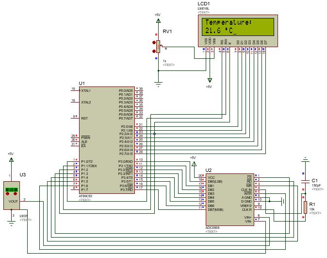
84 83
EEE3410 Microcontroller Applications Department of Electrical Engineering Lecture 4 The 8051 Architecture
 Department of Electrical Engineering Lecture 4 The 8051 Architecture 1 In this Lecture Overview General physical & operational features Block diagram Pin assignments Logic symbol Hardware description Pin
Microcontroller Intel [Instruction Set]
![Microcontroller Intel [Instruction Set]](/thumbs/82/86620819.jpg "Microcontroller Intel [Instruction Set]") Microcontroller Intel 8051 [Instruction Set] Structure of Assembly Language [ label: ] mnemonic [operands] [ ;comment ] Example: MOV R1, #25H ; load data 25H into R1 2 8051 Assembly Language Registers
Microcontroller Intel 8051 [Instruction Set] Structure of Assembly Language [ label: ] mnemonic [operands] [ ;comment ] Example: MOV R1, #25H ; load data 25H into R1 2 8051 Assembly Language Registers
Microprocessors 1. The 8051 Instruction Set. Microprocessors 1 1. Msc. Ivan A. Escobar Broitman
 Microprocessors 1 The 8051 Instruction Set Microprocessors 1 1 Instruction Groups The 8051 has 255 instructions Every 8-bit opcode from 00 to FF is used except for A5. The instructions are grouped into
 Contents 8051 Instruction Set BY D. BALAKRISHNA, Research Assistant, IIIT-H Chapter I : Control Transfer Instructions Lesson (a): Loop Lesson (b): Jump (i) Conditional Lesson (c): Lesson (d): Lesson (e):
Architecture & Instruction set of 8085 Microprocessor and 8051 Micro Controller
 of 8085 microprocessor 8085 is pronounced as "eighty-eighty-five" microprocessor. It is an 8-bit microprocessor designed by Intel in 1977 using NMOS technology. It has the following configuration 8-bit
8051 Overview and Instruction Set
 8051 Overview and Instruction Set Curtis A. Nelson Engr 355 1 Microprocessors vs. Microcontrollers Microprocessors are single-chip CPUs used in microcomputers Microcontrollers and microprocessors are different
8051 Microcontroller
 8051 Microcontroller EE4380 Fall 2001 Pari vallal Kannan Center for Integrated Circuits and Systems University of Texas at Dallas 8051 Architecture Programmer s View Register Set Instruction Set Memory
UNIT 2 THE 8051 INSTRUCTION SET AND PROGRAMMING
 UNIT 2 THE 8051 INSTRUCTION SET AND PROGRAMMING Instructions Alphabetical List of Instructions ACALL: Absolute Call ADD, ADDC: Add Accumulator (With Carry) AJMP: Absolute Jump ANL: Bitwise AND CJNE: Compare
Module Contents of the Module Hours COs
 Microcontrollers (EE45): Syllabus: Module Contents of the Module Hours COs 1 8051 MICROCONTROLLER ARCHITECTURE: Introduction to Microprocessors and Microcontrollers, the 8051 Architecture, 08 1 and pin
Memory organization Programming model - Program status word - register banks - Addressing modes - instruction set Programming examples.
 MICROCONTROLLERS AND APPLICATIONS 1 Module 2 Module-2 Contents: Memory organization Programming model - Program status word - register banks - Addressing modes - instruction set Programming examples. MEMORY
SN8F5000 Family Instruction Set
 SONiX Technology Co., Ltd. 8051-based Microcontroller 1 Overview SN8F5000 is 8051 Flash Type microcontroller supports comprehensive assembly instructions and which are fully compatible with standard 8051.
Microcontroller. Instruction set of 8051
 UNIT 2: Addressing Modes and Operations: Introduction, Addressing modes, External data Moves, Code Memory, Read Only Data Moves / Indexed Addressing mode, PUSH and POP Opcodes, Data exchanges, Example
Assembly Language programming (2)
") EEE3410 Microcontroller Applications LABORATORY Experiment 2 Assembly Language programming (2) Name Class Date Class No. Marks Arithmetic, Logic and Jump instructions Objectives To learn and practice the
EEE3410 Microcontroller Applications LABORATORY Experiment 2 Assembly Language programming (2) Name Class Date Class No. Marks Arithmetic, Logic and Jump instructions Objectives To learn and practice the
Programming of 8085 microprocessor and 8051 micro controller Study material
 8085 Demo Programs Now, let us take a look at some program demonstrations using the above instructions Adding Two 8-bit Numbers Write a program to add data at 3005H & 3006H memory location and store the
Digital Blocks Semiconductor IP
 805 SFR Bus Digital Blocks Semiconductor IP 805 Microcontroller Configurable Peripherals General Description The Digital Blocks (Configurable Peripherals) Microcontroller Verilog IP Core is complaint with
C51 Family. Architectural Overview of the C51 Family. Summary
 Architectural Overview of the C51 Family C51 Family Summary 1. Introduction............................................................ I.1. 1.1. TSC80C51/80C51/80C31.................................................................
UNIT THE 8051 INSTRUCTION SET AND PROGRAMMING
 UNIT THE 8051 INSTRUCTION SET AND PROGRAMMING Instructions Alphabetical List of Instructions ACALL: Absolute Call ADD, ADDC: Add Accumulator (With Carry) AJMP: Absolute Jump ANL: Bitwise AND CJNE: Compare
Digital Blocks Semiconductor IP
 Digital Blocks Semiconductor IP 805 Microcontroller General Description The Digital Blocks Microcontroller Verilog IP Core is complaint with the MCS 5 Instruction Set and contains standard 805 MCU peripherals,
TUTORIAL Assembly Language programming (2)
") 8051 Assembly Language programming (2) TUTORIAL 4 EEE3410 Microcontroller Applications 1. Write the instructions to move value 34h into register A and value 3Fh into register B, then add them together.
8051 Assembly Language programming (2) TUTORIAL 4 EEE3410 Microcontroller Applications 1. Write the instructions to move value 34h into register A and value 3Fh into register B, then add them together.
Digital Blocks Semiconductor IP
 Digital Blocks Semiconductor IP DB805C-FSM 805 Microcontroller FSM Finite State Machine General Description The Digital Blocks DB805C-FSM IP Core contains Digital Blocks compact DB805C CPU Core & GPIO
8051 Microcontroller
 8051 Microcontroller 1 Salient Features (1). 8 bit microcontroller originally developed by Intel in 1980. (2). High-performance CMOS Technology. (3). Contains Total 40 pins. (4). Address bus is of 16 bit
Q. Classify the instruction set of 8051 and list out the instructions in each type.
 INTRODUCTION Here is a list of the operands and their meanings: A - accumulator; Rn - is one of working registers (R0-R7) in the currently active RAM memory bank; Direct - is any 8-bit address register
ET355 Microprocessors Thursday 6:00 pm 10:20 pm
 ITT Technical Institute ET355 Microprocessors Thursday 6:00 pm 10:20 pm Unit 4 Chapter 6, pp. 139-174 Chapter 7, pp. 181-188 Unit 4 Objectives Lecture: BCD Programming Examples of the 805x Microprocessor
ENE 334 Microprocessors
 Page 1 ENE 334 Microprocessors Lecture 10: MCS-51: Logical and Arithmetic : Dejwoot KHAWPARISUTH http://webstaff.kmutt.ac.th/~dejwoot.kha/ ENE 334 MCS-51 Logical & Arithmetic Page 2 Logical: Objectives
CS 320. Computer Architecture Core Architecture
 CS 320 Computer Architecture 8051 Core Architecture Evan Hallam 19 April 2006 Abstract The 8051 is an 8-bit microprocessor designed originally in the 1980 s by the Intel Corporation. This inexpensive and
DR bit RISC Microcontroller. Instructions set details ver 3.10
 DR80390 8-bit RISC Microcontroller Instructions set details ver 3.10 DR80390 Instructions set details - 2 - Contents 1. Overview 7 1.1. Document structure. 7 2. Instructions set brief 7 2.1. Instruction
ET2640 Microprocessors
 ET2640 Microprocessors Unit -2 Processor Programming Concepts Basic Control Instructor : Stan Kong Email : skong@itt-tech.edu Figure 2 4 Bits of the PSW Register 8051 REGISTER BANKS AND STACK 80 BYTES
Principle and Interface Techniques of Microcontroller
 Principle and Interface Techniques of Microcontroller --8051 Microcontroller and Embedded Systems Using Assembly and C LI, Guang ( 李光 ) Prof. PhD, DIC, MIET WANG, You ( 王酉 ) PhD, MIET 杭州 浙江大学 2011 Chapter
Dragonchip. Instruction Set Manual
 Dragonchip Instruction Set Manual Version 3.1 July 2004 The Objective of this document is to provide the user a detail description to the each instruction set used in Dragonchip s MCU family. There are
8051 microcontrollers
 8051 microcontrollers Presented by: Deepak Kumar Rout Synergy Institute of Engineering and Technology, Dhenkanal Chapter 2 Introduction Intel MCS-51 family of microcontrollers consists of various devices
Microcontroller and Embedded Systems:
 Microcontroller and Embedded Systems: Branches: 1. Electronics & Telecommunication Engineering 2. Electrical & Electronics Engineering Semester: 6 th Semester / 7 th Semester 1. Explain the differences
TUTORIAL. Donal Heffernan University of Limerick May Tutorial D.Heffernan 2000,
 8051 TUTORIAL Donal Heffernan University of Limerick May-2002 8051 Tutorial D.Heffernan 2000, 2001 1 Blank 8051 Tutorial D.Heffernan 2000, 2001 2 Some reference material: Test books + MacKenzie Scott.
Introduction To MCS-51
 Introduction To MCS-51 By Charoen Vongchumyen Department of Computer Engineering Faculty of Engineering KMITLadkrabang 8051 Hardware Basic Content Overview Architechture Memory map Register Interrupt Timer/Counter
8051 Microcontroller
 8051 Microcontroller The 8051, Motorola and PIC families are the 3 leading sellers in the microcontroller market. The 8051 microcontroller was originally developed by Intel in the late 1970 s. Today many
Embedded Controller Programming
 Embedded Controller Programming Counters, Timers and I/O in Assembly Language Ken Arnold Copyright 2000-2004 Ken Arnold 1 Outline Timer/Counters Serial Port More 8051 Instructions Examples Copyright 2000-2004
MASSEY UNIVERSITY PALMERSTON NORTH CAMPUS
 MASSEY UNIVERSITY PALMERSTON NORTH CAMPUS EXAMINATION FOR 159.233 COMPUTER SYSTEMS Semester One June 2008 Time allowed: THREE (3) hours This exam contains THREE (3) questions ANSWER ALL THREE (3) QUESTIONS
Assembly Language programming (3)
") EEE3410 Microcontroller Applications LABORATORY Experiment 3 Assembly Language programming (3) Name Class Date Class No. Marks Conditional Program Branching and Subroutine Call in 8051 Objectives To learn
EEE3410 Microcontroller Applications LABORATORY Experiment 3 Assembly Language programming (3) Name Class Date Class No. Marks Conditional Program Branching and Subroutine Call in 8051 Objectives To learn
CHAPTER ASSEMBLY LANGUAGE PROGRAMMING
 CHAPTER 2 8051 ASSEMBLY LANGUAGE PROGRAMMING Registers Register are used to store information temporarily: A byte of data to be processed An address pointing to the data to be fetched The vast majority
e-pg Pathshala Subject : Computer Science Paper: Embedded System Module: 8051 Architecture Module No: CS/ES/5 Quadrant 1 e-text
 e-pg Pathshala Subject : Computer Science Paper: Embedded System Module: 8051 Architecture Module No: CS/ES/5 Quadrant 1 e-text In this lecture the detailed architecture of 8051 controller, register bank,
Control Transfer Instructions Jump, Loop, and Call. ECE473/573 Microprocessor System Design, Dr. Shiue
 Control Transfer Instructions Jump, Loop, and Call 1 Jump Instructions JZ label ; Jump if A=0 JNZ label ; Jump if A!=0 DJNZ reg, label ; Decrement and Jump if A (or reg.)!=0 CJNE A, byte ; Compare and
MICROCONTROLLER AND PLC LAB-436 SEMESTER-5
 MICROCONTROLLER AND PLC LAB-436 SEMESTER-5 Exp:1 STUDY OF MICROCONTROLLER 8051 To study the microcontroller and familiarize the 8051microcontroller kit Theory:- A Microcontroller consists of a powerful
EXPERIMENT NO.1. A Microcontroller is a complete computer system built on a single chip.
 EXPERIMENT NO.1 AIM: Study of 8051 Microcontroller TOOLS: 8051 kit THEORY: Salient Features of 8051 A Microcontroller is a complete computer system built on a single chip. It contains all components like
Question Bank Microprocessor and Microcontroller
 QUESTION BANK - 2 PART A 1. What is cycle stealing? (K1-CO3) During any given bus cycle, one of the system components connected to the system bus is given control of the bus. This component is said to
8051 Microcontrollers
 8051 Microcontrollers Richa Upadhyay Prabhu NMIMS s MPSTME richa.upadhyay@nmims.edu March 8, 2016 Controller vs Processor Controller vs Processor Introduction to 8051 Micro-controller In 1981,Intel corporation
Dodatak. Skup instrukcija
 Dodatak Skup instrukcija Arithmetic Operations [@Ri] implies contents of memory location pointed to by R0 or R1 Rn refers to registers R0-R7 of the currently selected register bank 2 ADD A,
Module I. Microcontroller can be classified on the basis of their bits processed like 8bit MC, 16bit MC.
 MICROCONTROLLERS AND APPLICATIONS 1 Module 1 Module I Introduction to Microcontrollers: Comparison with Microprocessors Harvard and Von Neumann Architectures - 80C51 microcontroller features - internal
Programming Book Microcontroller Kit. Rev 3.0 January, Wichit Sirichote
 Programming Book1 8051 Microcontroller Kit Rev 3.0 January, 016 016 Wichit Sirichote 1 Contents Overview...3 SAFTY INFORMATION...3 Tools...3 Experiment 1 Blinking LED...4 Experiment Binary number counting...9
MCS -51 Programmer s Guide and Instruction Set
 MCS -51 Programmer s Guide and Instruction Set November 1992 Order Number 270249-003 COPYRIGHT INTEL CORPORATION 1996 MCS -51 PROGRAMMER S GUIDE AND INSTRUCTION SET CONTENTS PAGE MEMORY ORGANIZATION 1
~: Simple Programs in 8051 assembly language :~
 ~: Simple Programs in 8051 assembly language :~ Here some simple programs of 8051 are given to understand the operation of different instructions and to understand the logic behind particular program.
8051 Microcontroller Assembly Programming
 8051 Microcontroller Assembly Programming EE4380 Fall 2002 Class 3 Pari vallal Kannan Center for Integrated Circuits and Systems University of Texas at Dallas Topics Machine code 8051 Addressing Modes
Chapter 3. Bit Addressable Area. By DeccanRobots
 Chapter 3 Bit Addressable Area By DeccanRobots What is Bit Addressable Area? FFh 2Fh 20h 00h Data Memory General purpose Memory Area Bit Addressable Memory Registers Memory Area from 20H to 2FH is Bit
ELEG3924 Microprocessor
 Department of Electrical Engineering University of Arkansas ELEG3924 Microprocessor Ch.2 Assembly Language Programming Dr. Jing Yang jingyang@uark.edu 1 OUTLINE Inside 8051 Introduction to assembly programming
8051 Core Specification
 8051 Core Specification Authors: Jaka Simsic Simon Teran jakas@opencores.org simont@opencores.org Rev. 0.1 August 14, 2001 First Draft www.opencores.org Rev 0.1 First Draft 1 of 26 Revision History Rev.
Chapter Family Microcontrollers Instruction Set
 Chapter 4 8051 Family Microcontrollers Instruction Set Lesson 5 Program Flow Control and Interrupt Flow Control Instructions 2 Branch instructions- Jump to new value of Program Counter (PC) LJMP address16
Instruction Set Of 8051
 Instruction Set Of 8051 By Darshan Patel M.Tech (Power Electronics & Drives) Assistant Professor, Electrical Department Sankalchand Patel college of Engineering-Visnagar Introduction The process of writing
8051 Microcontrollers
 8051 Microcontrollers Richa Upadhyay Prabhu NMIMS s MPSTME richa.upadhyay@nmims.edu March 15, 2016 8051 INSTRUCTIONS JUMP, LOOP AND CALL INSTRUCTIONS 8051 INSTRUCTIONS Repeating a sequence of instructions
MODULE-1. Short Answer Questions
 MODULE-1 Short Answer Questions 1. Give the comparison between microprocessor and microcontroller. It is very clear from figure that in microprocessor we have to interface additional circuitry for providing
Application Brief D-005
 Interfacing the Avago HDSP-2xxx LED Alphanumeric Displays with the Intel 8751H Microcontroller Application Brief D-005 Introduction The HDSP-21xx/-25xx series of products is ideal for applications where
Engr. A. N. Aniedu Electronic and Computer Engineering Nnamdi Azikiwe University, Awka
 Engr. A. N. Aniedu Electronic and Computer Engineering Nnamdi Azikiwe University, Awka INTRODUCTION Microcontroller vs General Purpose Microprocessor General-purpose microprocessors contains No RAM No
SOLUTION MANUAL FOR THE 8051 MICROCONTROLLER 4TH EDITION BY MACKENZIE AND PHAN
 SOLUTION MANUAL FOR THE 8051 MICROCONTROLLER 4TH EDITION BY MACKENZIE AND PHAN Chapter 1 - Introduction to Microcontrollers 1. (a)the first widely used microprocessor was the 8080. (b) The 8080 was introduced
What Registers are available? Programming in Assembler. Assembler Programming - like early Basic. Assembler Data Movement Instructions
 Programming in Assembler Need knowledge of CPU 8051 Programmers model what registers are available? what memory is available? code memory (for programs) data memory (for variables and the stack) what instructions
Practical Course File For
 Practical Course File For Microprocessor (IT 473) B.Tech (IT) IV-SEM Department of IT University Institute of Engineering & Technology Panjab University, Chandigarh Page 1 INTRODUCTION... 4 EXPERIMENT-1:
ELEG3924 Microprocessor
 Department of Electrical Engineering University of Arkansas ELEG3924 Microprocessor Ch.3 Jump, Loop, and Call Dr. Jing Yang jingyang@uark.edu 1 OUTLINE Loop and Jump instructions Call instructions Time
ELEG3923 Microprocessor Ch.6 Arithmetic and Logics
 Department of Electrical Engineering University of Arkansas ELEG3923 Microprocessor Ch.6 Arithmetic and Logics Dr. Jingxian Wu wuj@uark.edu OUTLINE 2 Arithmetic instructions Signed number operations Logic
MICROPROCESSOR & MICROCONTROLLER
 a) From road north to East From road east to north From road south to west From road west to south From road west to north b) From road north to East From road south to west From road south to north From
8051 Programming: Arithmetic and Logic
 8051 Programming: Arithmetic and Logic EE4380 Fall 2002 Class 4 Pari vallal Kannan Center for Integrated Circuits and Systems University of Texas at Dallas Topics Signed and Unsigned arithmetic Binary
ELEG3923 Microprocessor Ch.2 Assembly Language Programming
 Department of Electrical Engineering University of Arkansas ELEG3923 Microprocessor Ch.2 Assembly Language Programming Dr. Jingxian Wu wuj@uark.edu OUTLINE 2 Inside 8051 Introduction to assembly programming
MICROPROCESSORS AND MICROCONTROLLERS MATERIAL. Features of 8051:
 DEPARTMENT OF ECE MICROPROCESSORS AND MICROCONTROLLERS MATERIAL UNIT V 8051 MICROCONTROLLERS To make a complete microcomputer system, only microprocessor is not sufficient. It is necessary to add other
UNIT MICROCONTROLLER AND ITS PROGRAMMING
 M i c r o p r o c e s s o r s a n d M i c r o c o n t r o l l e r s P a g e 1 UNIT-7 8051 MICROCONTROLLER AND ITS PROGRAMMING INTRODUCTION The microcontroller incorporates all the features that are found
80C51 family programmer s guide and instruction set. 80C51 Family. PROGRAMMER S GUIDE AND INSTRUCTION SET Memory Organization. Philips Semiconductors
 PROGRAMMER S GUIDE AND INSTRUCTION SET Memory Organization Program Memory The 80C51 has separate address spaces for program and data memory. The Program memory can be up to 64k bytes long. The lower 4k
Principle and Interface Techniques of Microcontroller
 Principle and Interface Techniques of Microcontroller --8051 Microcontroller and Embedded Systems Using Assembly and C LI, Guang ( 李光 ) Prof. PhD, DIC, MIET WANG, You ( 王酉 ) PhD, MIET 杭州 浙江大学 2014 Chapter
Three criteria in Choosing a Microcontroller
 The 8051 Microcontroller architecture Contents: Introduction Block Diagram and Pin Description of the 8051 Registers Some Simple Instructions Structure of Assembly language and Running an 8051 program
BHARATHIDASAN ENGINEERING COLLEGE. III Year / V Semester / EEE MICROPROCESSORS AND MICROCONTROLLERS (R-2013)
") BHARATHIDASAN ENGINEERING COLLEGE III Year / V Semester / EEE MICROPROCESSORS AND MICROCONTROLLERS (R-2013) FREQUENTLY ASKED QUESTIONS IN UNIVERSITY EXAMINATION PART A UNIT 1-8085 PROCESSOR 1. Draw the
BHARATHIDASAN ENGINEERING COLLEGE III Year / V Semester / EEE MICROPROCESSORS AND MICROCONTROLLERS (R-2013) FREQUENTLY ASKED QUESTIONS IN UNIVERSITY EXAMINATION PART A UNIT 1-8085 PROCESSOR 1. Draw the
The Microcontroller. Lecture Set 3. Major Microcontroller Families. Example Microcontroller Families Cont. Example Microcontroller Families
 The Microcontroller Lecture Set 3 Architecture of the 8051 Microcontroller Microcontrollers can be considered as self-contained systems with a processor, memory and I/O ports. In most cases, all that is
ELEG3923 Microprocessor Ch.3 Jump, Loop, and Call
 Department of Electrical Engineering University of Arkansas ELEG3923 Microprocessor Ch.3 Jump, Loop, and Call Dr. Jingxian Wu wuj@uark.edu OUTLINE 2 Loop and Jump instructions Call instructions Time delay
8051 Programming using Assembly
 8051 Programming using Assembly The Instruction Addressing Modes dest,source ; dest = source A,#72H ;A=72H A, # r ;A= r OR 72H R4,#62H ;R4=62H B,0F9H ;B=the content of F9 th byte of RAM DPTR,#7634H DPL,#34H
Assembly Language Programming of 8085
 Assembly Language Programming of 8085 Topics 1. Introduction 2. Programming model of 8085 3. Instruction set of 8085 4. Example Programs 5. Addressing modes of 8085 6. Instruction & Data Formats of 8085
UNIT-III ASSEMBLY LANGUAGE PROGRAMMING. The CPU can access data in various ways, which are called addressing modes
 8051 Software Overview: 1. Addressing Modes 2. Instruction Set 3. Programming 8051 Addressing Modes: UNIT-III ASSEMBLY LANGUAGE PROGRAMMING The CPU can access data in various ways, which are called addressing
8-bit Microcontroller with 8K Bytes In-System Programmable Flash AT89S52
 Features Compatible with MCS -51 Products 8K Bytes of In-System Programmable (ISP) Flash Memory Endurance: 10,000 Write/Erase Cycles 4.0V to 5.5V Operating Range Fully Static Operation: 0 Hz to 33 MHz
EE6502- MICROPROCESSOR AND MICROCONTROLLER
 . EE6502- MICROPROCESSOR AND MICROCONTROLLER UNIT III - 8051 MICROCONTROLLER PART - A 1. What is Microcontroller? A device which contains the microprocessor with integrated peripherals like memory, serial
UNIT IV MICROCONTROLLER
 UNIT IV 8051- MICROCONTROLLER Prepared by R. Kavitha Page 1 Application Prepared by R. Kavitha Page 2 Pin Description of the 8051 UNIT IV- 8051 MICROCONTROLLER P1.0 P1.1 P1.2 P1.3 P1.4 P1.5 P1.6 P1.7 RST
Arithmetic and Logic
 8051 - Arithmetic and Logic EE4380 Fall 2001 Class 8 Pari vallal Kannan Center for Integrated Circuits and Systems University of Texas at Dallas Signed Arithmetic - Concepts Representation of the sign
 8051 Memory Organization BY D. BALAKRISHNA, Research Assistant, IIIT-H Chapter 1: Memory Organization There are 2 types of memories available in 8051 microcontroller. Program memory/c code memory (ROM)
CPEG300 Embedded System Design. Lecture 3 Memory
 CPEG300 Embedded System Design Lecture 3 Memory Hamad Bin Khalifa University, Spring 2018 Review Von Neumann vs. Harvard architecture? System on Board, system on chip? Generic Hardware Architecture of
Q.1. A) Attempt any THREE of the following:
 Attempt any THREE of the following:") Important Instructions to examiners: 1) The answers should be examined by key words and not as word-to-word as given in the model answer scheme. 2) The model answer and the answer written by candidate
Important Instructions to examiners: 1) The answers should be examined by key words and not as word-to-word as given in the model answer scheme. 2) The model answer and the answer written by candidate
Embedded World Television, Radio, CD player, Washing Machine Microwave Oven Card readers, Palm devices
 A presentation on INTRODUCTION We are living in the Embedded World. We are surrounded with many embedded products and our daily life largely depends on the proper functioning of these gadgets. Television,
SYLLABUS UNIT - I 8086/8088 ARCHITECTURE AND INSTRUCTION SET
 1 SYLLABUS UNIT - I 8086/8088 ARCHITECTURE AND INSTRUCTION SET Intel 8086/8088 Architecture Segmented Memory, Minimum and Maximum Modes of Operation, Timing Diagram, Addressing Modes, Instruction Set,
CPEG300 Embedded System Design. Lecture 6 Interrupt System
 CPEG300 Embedded System Design Lecture 6 Interrupt System Hamad Bin Khalifa University, Spring 2018 Correction Lecture 3, page 18: Only direct addressing mode is allowed for pushing or popping the stack:
Understanding the basic building blocks of a microcontroller device in general. Knows the terminologies like embedded and external memory devices,
 Understanding the basic building blocks of a microcontroller device in general. Knows the terminologies like embedded and external memory devices, CISC and RISC processors etc. Knows the architecture and
SUMMER 13 EXAMINATION
 MAHARASHTRA STATE BOARD OF TECHNICAL EDUCATION (Autonomous) (ISO/IEC - 27001-2005 Certified) Subject Code: 12187 SUMMER 13 EXAMINATION Model Answer Important Instructions to examiners: 1) The answers should
EXPERIMENT NO. 1 THE MKT 8085 MICROPROCESSOR TRAINER
 OBJECT: EXPERIMENT NO. 1 THE MKT 8085 MICROPROCESSOR TRAINER To understand the structure and operating instruction of the microprocessor trainer. INTRODUCTION: The MKT 8085 is a single-board microcomputer,
Vidyalankar T.E. Sem. V [ETRX] Microprocessors and Microcontrollers I Prelim Question Paper Solution
![Vidyalankar T.E. Sem. V [ETRX] Microprocessors and Microcontrollers I Prelim Question Paper Solution](/thumbs/74/70555699.jpg "Vidyalankar T.E. Sem. V [ETRX] Microprocessors and Microcontrollers I Prelim Question Paper Solution") 1. (a) 1. (b) T.E. Sem. V [ETRX] Microprocessors and Microcontrollers I Prelim Question Paper Solution Priority modes. 1) Fully Nested Mode : It is a general purpose mode. IR 0 highest priority IR 1 lowest
1. (a) 1. (b) T.E. Sem. V [ETRX] Microprocessors and Microcontrollers I Prelim Question Paper Solution Priority modes. 1) Fully Nested Mode : It is a general purpose mode. IR 0 highest priority IR 1 lowest
Interrupt Programming: Interrupts vs. Polling Method:
 UNIT 4: INTERRUPT PROGRAMMING & SERIAL COMMUNICATION WITH 8051: Definition of an interrupt, types of interrupts, Timers and Counter programming with interrupts in assembly. 8051 Serial Communication: Data
MCS-51 Serial Port A T 8 9 C 5 2 1
 MCS-51 Serial Port AT89C52 1 Introduction to Serial Communications Serial vs. Parallel transfer of data Simplex, Duplex and half-duplex modes Synchronous, Asynchronous UART Universal Asynchronous Receiver/Transmitter.
Highlights. FP51 (FPGA based 1T 8051 core)
") Copyright 2017 PulseRain Technology, LLC. FP51 (FPGA based 1T 8051 core) 10555 Scripps Trl, San Diego, CA 92131 858-877-3485 858-408-9550 http://www.pulserain.com Highlights 1T 8051 Core Intel MCS-51 Compatible
Copyright 2017 PulseRain Technology, LLC. FP51 (FPGA based 1T 8051 core) 10555 Scripps Trl, San Diego, CA 92131 858-877-3485 858-408-9550 http://www.pulserain.com Highlights 1T 8051 Core Intel MCS-51 Compatible
CoE3DJ4 Digital Systems Design. Chapter 5: Serial Port Operation
 CoE3DJ4 Digital Systems Design Chapter 5: Serial Port Operation Serial port 8051 includes an on-chip serial port Hardware access to the port is through TXD and RXD (Port 3 bits 1 and 0) Serial port is
EC2304-MICROPROCESSOR AND MICROCONROLLERS 2 marks questions and answers UNIT-I
 EC2304-MICROPROCESSOR AND MICROCONROLLERS 2 marks questions and answers 1. Define microprocessors? UNIT-I A semiconductor device(integrated circuit) manufactured by using the LSI technique. It includes
1. INTRODUCTION TO MICROPROCESSOR AND MICROCOMPUTER ARCHITECTURE:
 1. INTRODUCTION TO MICROPROCESSOR AND MICROCOMPUTER ARCHITECTURE: A microprocessor is a programmable electronics chip that has computing and decision making capabilities similar to central processing unit
1 MALP ( ) Unit-1. (1) Draw and explain the internal architecture of 8085.
 Unit-1. (1) Draw and explain the internal architecture of 8085.") (1) Draw and explain the internal architecture of 8085. The architecture of 8085 Microprocessor is shown in figure given below. The internal architecture of 8085 includes following section ALU-Arithmetic
(1) Draw and explain the internal architecture of 8085. The architecture of 8085 Microprocessor is shown in figure given below. The internal architecture of 8085 includes following section ALU-Arithmetic
Microcontroller and Applications
 S.Y. Diploma : Sem. IV [DE/EJ/ET/EN/EX/EQ/IS/IC/IE] Microcontroller and Applications Time: 3 Hrs.] Prelim Question Paper Solution [Marks : 70 Q.1 Attempt any FIVE of the following : [10] Q.1(a) Define