Xilinx ASMBL Architecture
|
|
|
- Jason Gibson
- 6 years ago
- Views:
Transcription

1 FPGA Structure

2 Xilinx ASMBL Architecture
3 Design Flow Synthesis: HDL to FPGA primitives Translate: FPGA Primitives to FPGA Slice components Map: Packing of Slice components into Slices, placement of Slices on fabric Route: connecting Slices Bitstream generation: generating the required configuration bits to load into the FPGA

4 Configurable Logic Blocks
5 Slice LUTs 1 CLB = 2 Slices 1 Slice = 4 LUT Modules, 2 MUXF7, 1 MUXF8 A LUT Module contains: 1 LUT6, 1 MUXCY, 1 XORCY, 2 FFs
6 Slice LUTs 1 CLB = 2 Slices 1 Slice = 4 LUT Modules, 2 MUXF7, 1 MUXF8 A LUT Module contrains: 1 LUT6, 1 MUXCY, 1 XORCY, 2 FFs
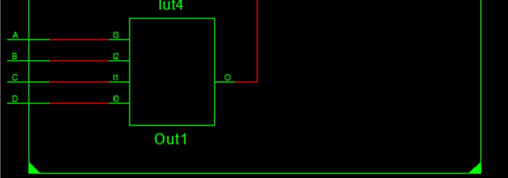
7 Slice LUTs LUTs = Multiplexers Data Inputs from the FPGA configuration bits Selection inputs from user logic For N-input LUT, 2 N configuration bits A B A B A B MUX 4:1 A B
8 Slice LUTs Number of LUT inputs is architecture dependent: Xilinx Virtex 4 and earlier: 4-input LUTs (LUT4), 2 LUTs per Slice Xilinx Virtex 5 and later: 6-input LUTs (LUT6), 4 LUTs per Slice Xilinx Virtex 6 and 7-Series: 6-input LUTs, configurable as two shared-input 5-input LUTs Altera: 8-input LUTs (ALM), configurable as combinations of smaller LUTs
9 Area and Delay vs. LUT Size LUTs have constant delay, regardless of implemented function Example: LUT4 architecture (Virtex4) O = I1 & I2 & I3 & I4 => 1 LUT, 0.43 ns O = I1 & I2 & I3 & I4 & I5 & I6 => 2 LUTs, 0.93 ns As a general rule: LUT delays are small, routing delays can be large
10 Exercise: Multiplexers Implementation of 2:1, 4:1, 8:1 multiplexers on Virtex-4 architecture Advanced multiplexing techniques: XAPP522
11 Slice Multiplexer Resources A slice contains multiplexers that mux between LUT outputs (MUXFx) Virtex-4: MUXF5 Virtex-5 and later: MUXF7, MUXF8
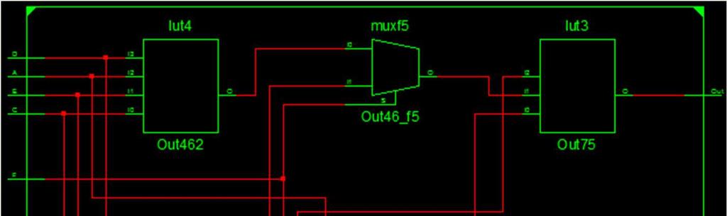
12 Logic optimization using MUXFx Example: LUT4 architecture (Virtex4) O = I1 & I2 & I3 & I4 & I5 => 1 LUT, 1 MUXF5, 0.72ns Use of MUXFx reduces LUT usage and routing requirements Local (in-slice) routing -> more predictable performance
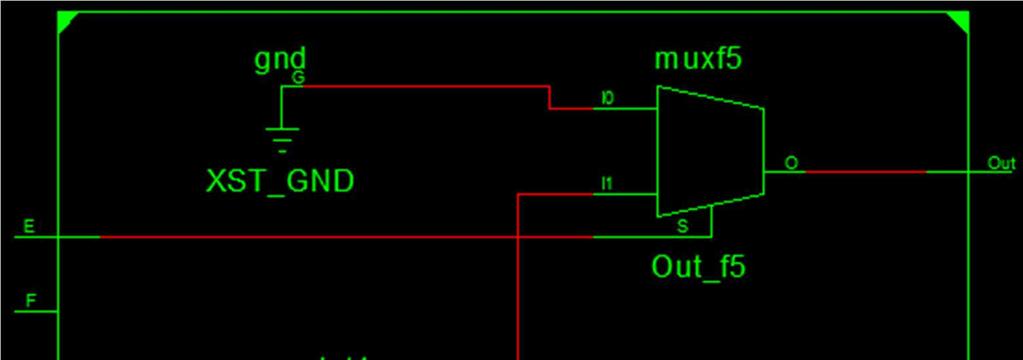
13 Logic optimization using MUXFx
14 Multiplexers vs First Index Decoders Example code: if(a) Out = E F; else if(b) Out = E & F; else if(c) Out = E ^ F; else if(d) Out = ~E F; else Out = 1'bx;
15 Multiplexers vs First Index Decoders
16 Multiplexers vs. First Index Decoders The synthesis tool cannot always detect properties of the inputs of logic functions Inputs are from pins Inputs are from memories (Block or Distributed) Unconstrained version, for when we know {A,B,C,D} is one-hot: assign sel1 = ~(A B); assign sel0 = B D; case({sel1,sel0}) 2'b00: Out = E F; 2'b01: Out = E & F; 2'b10: Out = E ^ F; 2'b11: Out = ~E F; endcase
17 Multiplexers vs. First Index Decoders
18 Exercise: Adder LUT6 Architecture (7-Series) Implement 4-bit adder optimally (carry-chain versus carry look-ahead)


19 Slice Arithmetic Resources Carry-chain adder implementation
20 Slice Arithmetic Resources Slice primitives: MUXCY, XORCY
21 Selecting Adder Type Analysis of various adder types (Design and Performance Analysis of Various Adders using Verilog; M. SaiKumar, P. Samundiswary) Ripple-carry (RCA) has hardware support in FPGA Carry-save (CSA) / Carry-look-ahead (CLA) are first choice for VLSI Assignment: compare RCA/CSA based Popcount Implement Verilog for 16b input Synthesize/Map Record delay and LUT/Slice counts
22 Adder Inference Synthesis tools will infer RCA Multi-input adder implementation may be controlled through parentheses: E = (A+B)+(C+D) results in tree E= (A+(B+(C+D))) results in cascade
23 Optimization Example Implementing an increment instruction in a processor ALU in Virtex-4 Behavioral description in ISE 14.2 yields bad results for the following code: if(sel) else sum = a+b+carry_in; sum = a+4'd1+carry_in; 12 Slices, 1.5ns delay. Can we do better?
24 Optimization Results Using LUT3s instead of LUT2s in the adder structure, we can hardcode a multiplexer that selects between operand b and constant 1 before XOR-ing with operand a The rest of the structure is identical (MUXCY, XORCY) and built with primitive instantiation Results: 2 Slices, 1ns delay
25 Slice Registers Latch/FlipFlop primitives available within the Slice Available control signals: Set/Reset, Clock Enable, Clock Asynchronous/Synchronous Set/Reset Set/Reset typically refers to synchronous Clear/Preset refers to asynchronous Primitives: FD{R/S/RS/C/P}{E}
26 Slice Registers Synchronous Asynchronous Set clock) if(set) q<=1; else q<=d; clock or posedge set) if(set) q<=1; else q<=d; Reset clock) if(reset) q<=0; else q<=d; clock or negedge reset) if(set) q<=0; else q<=d;
27 Using Clock Enables Control signal priority determines implementation of the Flip-Flop primitive Example 1: Set before CE clk) if(set) q<=1; else if(ce) q<=d; Example 2: CE before Set clk) if(ce) if(set) q<=1; else q<=d;


28 Using Clock Enables Example 1 Results: FDSE Example 2 Results: FDE + LUT
29 Using Clock Enables Flip-Flop primitives are architecture dependent Example: clk) if(reset) q<=0; else if(set) q<=1; else if(ce) q <= d;


30 Using Clock Enables Spartan-3: FDRSE Virtex-6: LUT+FDR
31 Using Clock Enables Another example: clk) if(set) q<=1; else if(reset) q<=0; else if(ce) q <= d;

32 Using Clock Enables
33 Async vs Sync Resets Asynchronous resets Act immediately Are clock-independent Induce timing hazards Synchronous resets Ports can be used to minimize logic Predictable
34 Global Resets We use global resets to: Get the circuit into a known state at power-up Initialize simulations properly (!) Global resets have to be routed to S/R pins of the Flip-Flop FPGAs include a dedicated global set-reset net for post-configuration initialization (GSR)
35 Using the GSR STARTUP_VIRTEX6 #(.PROG_USR("FALSE") // Activate program event security feature ) STARTUP_VIRTEX6_inst (.CFGCLK(CFGCLK), // 1-bit Configuration main clock output.cfgmclk(cfgmclk), // 1-bit Configuration internal oscillator clock output.dinspi(dinspi), // 1-bit DIN SPI PROM access output.eos(eos), // 1-bit Active high output signal indicating the End Of Configuration..PREQ(PREQ), // 1-bit PROGRAM request to fabric output.tckspi(tckspi), // 1-bit TCK configuration pin access output.clk(clk), // 1-bit User start-up clock input.gsr(gsr), // 1-bit Global Set/Reset input (GSR cannot be used for the port name).gts(gts), // 1-bit Global 3-state input (GTS cannot be used for the port name).keyclearb(keyclearb), // 1-bit Clear AES Decrypter Key input from Battery-Backed RAM (BBRAM).PACK(PACK), // 1-bit PROGRAM acknowledge input.usrcclko(usrcclko), // 1-bit User CCLK input.usrcclkts(usrcclkts), // 1-bit User CCLK 3-state enable input.usrdoneo(usrdoneo), // 1-bit User DONE pin output control.usrdonets(usrdonets) // 1-bit User DONE 3-state enable output );
36 Avoid Latches! Latches are most commonly generated by unterminated control sequences Missing else statements in if clauses Missing default statements in case clauses To avoid over-constraining the logic, use x values in your else and default statements
Topics. Midterm Finish Chapter 7
 Lecture 9 Topics Midterm Finish Chapter 7 Xilinx FPGAs Chapter 7 Spartan 3E Architecture Source: Spartan-3E FPGA Family Datasheet CLB Configurable Logic Blocks Each CLB contains four slices Each slice
Topics. Midterm Finish Chapter 7
 Lecture 9 Topics Midterm Finish Chapter 7 ROM (review) Memory device in which permanent binary information is stored. Example: 32 x 8 ROM Five input lines (2 5 = 32) 32 outputs, each representing a memory
ECE 645: Lecture 1. Basic Adders and Counters. Implementation of Adders in FPGAs
 ECE 645: Lecture Basic Adders and Counters Implementation of Adders in FPGAs Required Reading Behrooz Parhami, Computer Arithmetic: Algorithms and Hardware Design Chapter 5, Basic Addition and Counting,
HDL Coding Style Xilinx, Inc. All Rights Reserved
 HDL Coding Style Objective After completing this module, you will be able to: Select a proper coding style to create efficient FPGA designs Specify Xilinx resources that need to be instantiated for various
FPGA architecture and design technology
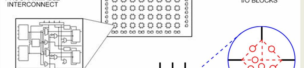
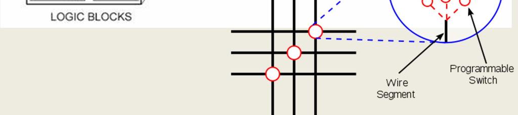
 CE 435 Embedded Systems Spring 2017 FPGA architecture and design technology Nikos Bellas Computer and Communications Engineering Department University of Thessaly 1 FPGA fabric A generic island-style FPGA
TSEA44 - Design for FPGAs
 2015-11-24 Now for something else... Adapting designs to FPGAs Why? Clock frequency Area Power Target FPGA architecture: Xilinx FPGAs with 4 input LUTs (such as Virtex-II) Determining the maximum frequency
Block RAM. Size. Ports. Virtex-4 and older: 18Kb Virtex-5 and newer: 36Kb, can function as two 18Kb blocks
 Block RAM Dedicated FPGA resource, separate columns from CLBs Designed to implement large (Kb) memories Multi-port capabilities Multi-clock capabilities FIFO capabilities Built-in error detection and correction
! Program logic functions, interconnect using SRAM. ! Advantages: ! Re-programmable; ! dynamically reconfigurable; ! uses standard processes.
 Topics! SRAM-based FPGA fabrics:! Xilinx.! Altera. SRAM-based FPGAs! Program logic functions, using SRAM.! Advantages:! Re-programmable;! dynamically reconfigurable;! uses standard processes.! isadvantages:!
Verilog Sequential Logic. Verilog for Synthesis Rev C (module 3 and 4)
") Verilog Sequential Logic Verilog for Synthesis Rev C (module 3 and 4) Jim Duckworth, WPI 1 Sequential Logic Module 3 Latches and Flip-Flops Implemented by using signals in always statements with edge-triggered
Verilog Sequential Logic Verilog for Synthesis Rev C (module 3 and 4) Jim Duckworth, WPI 1 Sequential Logic Module 3 Latches and Flip-Flops Implemented by using signals in always statements with edge-triggered
Why Should I Learn This Language? VLSI HDL. Verilog-2
 Verilog Why Should I Learn This Language? VLSI HDL Verilog-2 Different Levels of Abstraction Algorithmic the function of the system RTL the data flow the control signals the storage element and clock Gate
FPGA for Complex System Implementation. National Chiao Tung University Chun-Jen Tsai 04/14/2011
 FPGA for Complex System Implementation National Chiao Tung University Chun-Jen Tsai 04/14/2011 About FPGA FPGA was invented by Ross Freeman in 1989 SRAM-based FPGA properties Standard parts Allowing multi-level
CSE140L: Components and Design Techniques for Digital Systems Lab
 CSE140L: Components and Design Techniques for Digital Systems Lab Tajana Simunic Rosing Source: Vahid, Katz, Culler 1 Announcements & Outline Lab 4 due; demo signup times listed on the cse140l site Check
EEL 4783: HDL in Digital System Design
 EEL 4783: HDL in Digital System Design Lecture 15: Logic Synthesis with Verilog Prof. Mingjie Lin 1 Verilog Synthesis Synthesis vs. Compilation Descriptions mapped to hardware Verilog design patterns for
INTRODUCTION TO FPGA ARCHITECTURE
 3/3/25 INTRODUCTION TO FPGA ARCHITECTURE DIGITAL LOGIC DESIGN (BASIC TECHNIQUES) a b a y 2input Black Box y b Functional Schematic a b y a b y a b y 2 Truth Table (AND) Truth Table (OR) Truth Table (XOR)
CSE140L: Components and Design
 CSE140L: Components and Design Techniques for Digital Systems Lab Tajana Simunic Rosing Source: Vahid, Katz, Culler 1 Grade distribution: 70% Labs 35% Lab 4 30% Lab 3 20% Lab 2 15% Lab 1 30% Final exam
PINE TRAINING ACADEMY
 PINE TRAINING ACADEMY Course Module A d d r e s s D - 5 5 7, G o v i n d p u r a m, G h a z i a b a d, U. P., 2 0 1 0 1 3, I n d i a Digital Logic System Design using Gates/Verilog or VHDL and Implementation
Synthesis vs. Compilation Descriptions mapped to hardware Verilog design patterns for best synthesis. Spring 2007 Lec #8 -- HW Synthesis 1
 Verilog Synthesis Synthesis vs. Compilation Descriptions mapped to hardware Verilog design patterns for best synthesis Spring 2007 Lec #8 -- HW Synthesis 1 Logic Synthesis Verilog and VHDL started out
ECE 545 Lecture 12. FPGA Resources. George Mason University
 ECE 545 Lecture 2 FPGA Resources George Mason University Recommended reading 7 Series FPGAs Configurable Logic Block: User Guide Overview Functional Details 2 What is an FPGA? Configurable Logic Blocks
DSP Resources. Main features: 1 adder-subtractor, 1 multiplier, 1 add/sub/logic ALU, 1 comparator, several pipeline stages
 DSP Resources Specialized FPGA columns for complex arithmetic functionality DSP48 Tile: two DSP48 slices, interconnect Each DSP48 is a self-contained arithmeticlogical unit with add/sub/multiply/logic
Verilog for High Performance
 Verilog for High Performance Course Description This course provides all necessary theoretical and practical know-how to write synthesizable HDL code through Verilog standard language. The course goes
EECS150 - Digital Design Lecture 5 - Verilog Logic Synthesis
 EECS150 - Digital Design Lecture 5 - Verilog Logic Synthesis Jan 31, 2012 John Wawrzynek Spring 2012 EECS150 - Lec05-verilog_synth Page 1 Outline Quick review of essentials of state elements Finite State
Lecture 3. Behavioral Modeling Sequential Circuits. Registers Counters Finite State Machines
 Lecture 3 Behavioral Modeling Sequential Circuits Registers Counters Finite State Machines Behavioral Modeling Behavioral Modeling Behavioral descriptions use the keyword always, followed by optional event
FPGA Design Challenge :Techkriti 14 Digital Design using Verilog Part 1
 FPGA Design Challenge :Techkriti 14 Digital Design using Verilog Part 1 Anurag Dwivedi Digital Design : Bottom Up Approach Basic Block - Gates Digital Design : Bottom Up Approach Gates -> Flip Flops Digital
Logic Synthesis. EECS150 - Digital Design Lecture 6 - Synthesis
 Logic Synthesis Verilog and VHDL started out as simulation languages, but quickly people wrote programs to automatically convert Verilog code into low-level circuit descriptions (netlists). EECS150 - Digital
N-input EX-NOR gate. N-output inverter. N-input NOR gate
 Hardware Description Language HDL Introduction HDL is a hardware description language used to design and document electronic systems. HDL allows designers to design at various levels of abstraction. It
Review from last time. CS152 Computer Architecture and Engineering Lecture 6. Verilog (finish) Multiply, Divide, Shift
 Multiply, Divide, Shift") Review from last time CS152 Computer Architecture and Engineering Lecture 6 Verilog (finish) Multiply, Divide, Shift February 11, 2004 John Kubiatowicz (www.cs.berkeley.edu/~kubitron) lecture slides: http://www-inst.eecs.berkeley.edu/~cs152/
Review from last time CS152 Computer Architecture and Engineering Lecture 6 Verilog (finish) Multiply, Divide, Shift February 11, 2004 John Kubiatowicz (www.cs.berkeley.edu/~kubitron) lecture slides: http://www-inst.eecs.berkeley.edu/~cs152/
Note: Closed book no notes or other material allowed, no calculators or other electronic devices.
 ECE 574: Modeling and Synthesis of Digital Systems using Verilog and VHDL Fall 2017 Exam Review Note: Closed book no notes or other material allowed, no calculators or other electronic devices. One page
Verilog Fundamentals. Shubham Singh. Junior Undergrad. Electrical Engineering
 Verilog Fundamentals Shubham Singh Junior Undergrad. Electrical Engineering VERILOG FUNDAMENTALS HDLs HISTORY HOW FPGA & VERILOG ARE RELATED CODING IN VERILOG HDLs HISTORY HDL HARDWARE DESCRIPTION LANGUAGE
FPGA for Software Engineers
 FPGA for Software Engineers Course Description This course closes the gap between hardware and software engineers by providing the software engineer all the necessary FPGA concepts and terms. The course
Digital Design with SystemVerilog
 Digital Design with SystemVerilog Prof. Stephen A. Edwards Columbia University Spring 25 Synchronous Digital Design Combinational Logic Sequential Logic Summary of Modeling Styles Testbenches Why HDLs?
Field Programmable Gate Array (FPGA)
") Field Programmable Gate Array (FPGA) Lecturer: Krébesz, Tamas 1 FPGA in general Reprogrammable Si chip Invented in 1985 by Ross Freeman (Xilinx inc.) Combines the advantages of ASIC and uc-based systems
Field Programmable Gate Array (FPGA) Lecturer: Krébesz, Tamas 1 FPGA in general Reprogrammable Si chip Invented in 1985 by Ross Freeman (Xilinx inc.) Combines the advantages of ASIC and uc-based systems
EECS150 - Digital Design Lecture 10 Logic Synthesis
 EECS150 - Digital Design Lecture 10 Logic Synthesis September 26, 2002 John Wawrzynek Fall 2002 EECS150 Lec10-synthesis Page 1 Logic Synthesis Verilog and VHDL stated out as simulation languages, but quickly
Verilog Tutorial. Introduction. T. A.: Hsueh-Yi Lin. 2008/3/12 VLSI Digital Signal Processing 2
 Verilog Tutorial T. A.: Hsueh-Yi Lin Introduction 2008/3/12 VLSI Digital Signal Processing 2 Verilog: A common language for industry HDL is a common way for hardware design Verilog VHDL Verilog is widely
EECS150 - Digital Design Lecture 10 Logic Synthesis
 EECS150 - Digital Design Lecture 10 Logic Synthesis February 13, 2003 John Wawrzynek Spring 2003 EECS150 Lec8-synthesis Page 1 Logic Synthesis Verilog and VHDL started out as simulation languages, but
Virtex-II Architecture
 Virtex-II Architecture Block SelectRAM resource I/O Blocks (IOBs) edicated multipliers Programmable interconnect Configurable Logic Blocks (CLBs) Virtex -II architecture s core voltage operates at 1.5V
Logic Circuits II ECE 2411 Thursday 4:45pm-7:20pm. Lecture 3
 Logic Circuits II ECE 2411 Thursday 4:45pm-7:20pm Lecture 3 Lecture 3 Topics Covered: Chapter 4 Discuss Sequential logic Verilog Coding Introduce Sequential coding Further review of Combinational Verilog
Chapter 9: Sequential Logic Modules
 Chapter 9: Sequential Logic Modules Prof. Soo-Ik Chae Digital System Designs and Practices Using Verilog HDL and FPGAs @ 2008, John Wiley 9-1 Objectives After completing this chapter, you will be able
Lecture 12 VHDL Synthesis
 CPE 487: Digital System Design Spring 2018 Lecture 12 VHDL Synthesis Bryan Ackland Department of Electrical and Computer Engineering Stevens Institute of Technology Hoboken, NJ 07030 1 What is Synthesis?
FPGA: What? Why? Marco D. Santambrogio
 FPGA: What? Why? Marco D. Santambrogio marco.santambrogio@polimi.it 2 Reconfigurable Hardware Reconfigurable computing is intended to fill the gap between hardware and software, achieving potentially much
Verilog for Synthesis Ing. Pullini Antonio
 Verilog for Synthesis Ing. Pullini Antonio antonio.pullini@epfl.ch Outline Introduction to Verilog HDL Describing combinational logic Inference of basic combinational blocks Describing sequential circuits
Field Programmable Gate Array
 Field Programmable Gate Array System Arch 27 (Fire Tom Wada) What is FPGA? System Arch 27 (Fire Tom Wada) 2 FPGA Programmable (= reconfigurable) Digital System Component Basic components Combinational
Chap 6 Introduction to HDL (d)
") Design with Verilog Chap 6 Introduction to HDL (d) Credit to: MD Rizal Othman Faculty of Electrical & Electronics Engineering Universiti Malaysia Pahang Ext: 6036 VERILOG HDL Basic Unit A module Module
Design with Verilog Chap 6 Introduction to HDL (d) Credit to: MD Rizal Othman Faculty of Electrical & Electronics Engineering Universiti Malaysia Pahang Ext: 6036 VERILOG HDL Basic Unit A module Module
Introduction to Field Programmable Gate Arrays
 Introduction to Field Programmable Gate Arrays Lecture 1/3 CERN Accelerator School on Digital Signal Processing Sigtuna, Sweden, 31 May 9 June 2007 Javier Serrano, CERN AB-CO-HT Outline Historical introduction.
ECE 448 Lecture 5. FPGA Devices
 E 448 Lecture 5 FPGA evices E 448 FPGA and ASIC esign with VHL George Mason University Required reading 7 Series FPGAs Configurable Logic Block: User Guide Overview Functional etails 2 What is an FPGA?
DESIGN AND IMPLEMENTATION OF ADDER ARCHITECTURES AND ANALYSIS OF PERFORMANCE METRICS
 International Journal of Electronics and Communication Engineering and Technology (IJECET) Volume 8, Issue 5, September-October 2017, pp. 1 6, Article ID: IJECET_08_05_001 Available online at http://www.iaeme.com/ijecet/issues.asp?jtype=ijecet&vtype=8&itype=5
Writing Circuit Descriptions 8
 8 Writing Circuit Descriptions 8 You can write many logically equivalent descriptions in Verilog to describe a circuit design. However, some descriptions are more efficient than others in terms of the
ECE 636. Reconfigurable Computing. Lecture 2. Field Programmable Gate Arrays I
 ECE 636 Reconfigurable Computing Lecture 2 Field Programmable Gate Arrays I Overview Anti-fuse and EEPROM-based devices Contemporary SRAM devices - Wiring - Embedded New trends - Single-driver wiring -
Altera FLEX 8000 Block Diagram
 Altera FLEX 8000 Block Diagram Figure from Altera technical literature FLEX 8000 chip contains 26 162 LABs Each LAB contains 8 Logic Elements (LEs), so a chip contains 208 1296 LEs, totaling 2,500 16,000
Synthesis Options FPGA and ASIC Technology Comparison - 1
 Synthesis Options Comparison - 1 2009 Xilinx, Inc. All Rights Reserved Welcome If you are new to FPGA design, this module will help you synthesize your design properly These synthesis techniques promote
VHDL for Synthesis. Course Description. Course Duration. Goals
 VHDL for Synthesis Course Description This course provides all necessary theoretical and practical know how to write an efficient synthesizable HDL code through VHDL standard language. The course goes
EECS150 - Digital Design Lecture 20 - Finite State Machines Revisited
 EECS150 - Digital Design Lecture 20 - Finite State Machines Revisited April 2, 2009 John Wawrzynek Spring 2009 EECS150 - Lec20-fsm Page 1 Finite State Machines (FSMs) FSM circuits are a type of sequential
Verilog 1 - Fundamentals
 Verilog 1 - Fundamentals FA FA FA FA module adder( input [3:0] A, B, output cout, output [3:0] S ); wire c0, c1, c2; FA fa0( A[0], B[0], 1 b0, c0, S[0] ); FA fa1( A[1], B[1], c0, c1, S[1] ); FA fa2( A[2],
Don t expect to be able to write and debug your code during the lab session.
 EECS150 Spring 2002 Lab 4 Verilog Simulation Mapping UNIVERSITY OF CALIFORNIA AT BERKELEY COLLEGE OF ENGINEERING DEPARTMENT OF ELECTRICAL ENGINEERING AND COMPUTER SCIENCE Lab 4 Verilog Simulation Mapping
Digital Integrated Circuits
 Digital Integrated Circuits Lecture 4 Jaeyong Chung System-on-Chips (SoC) Laboratory Incheon National University BCD TO EXCESS-3 CODE CONVERTER 0100 0101 +0011 +0011 0111 1000 LSB received first Chung
EECS150 - Digital Design Lecture 6 - Field Programmable Gate Arrays (FPGAs)
") EECS150 - Digital Design Lecture 6 - Field Programmable Gate Arrays (FPGAs) September 12, 2002 John Wawrzynek Fall 2002 EECS150 - Lec06-FPGA Page 1 Outline What are FPGAs? Why use FPGAs (a short history
EECS150 - Digital Design Lecture 6 - Field Programmable Gate Arrays (FPGAs) September 12, 2002 John Wawrzynek Fall 2002 EECS150 - Lec06-FPGA Page 1 Outline What are FPGAs? Why use FPGAs (a short history
An easy to read reference is:
 1. Synopsis: Timing Analysis and Timing Constraints The objective of this lab is to make you familiar with two critical reports produced by the Xilinx ISE during your design synthesis and implementation.
Basic FPGA Architecture Xilinx, Inc. All Rights Reserved
 Basic FPGA Architecture 2005 Xilinx, Inc. All Rights Reserved Objectives After completing this module, you will be able to: Identify the basic architectural resources of the Virtex -II FPGA List the differences
CSCB58 - Lab 3. Prelab /3 Part I (in-lab) /2 Part II (in-lab) /2 TOTAL /8
 /2 Part II (in-lab) /2 TOTAL /8") CSCB58 - Lab 3 Latches, Flip-flops, and Registers Learning Objectives The purpose of this exercise is to investigate the fundamental synchronous logic elements: latches, flip-flops, and registers. Prelab
CSCB58 - Lab 3 Latches, Flip-flops, and Registers Learning Objectives The purpose of this exercise is to investigate the fundamental synchronous logic elements: latches, flip-flops, and registers. Prelab
Verilog Module 1 Introduction and Combinational Logic
 Verilog Module 1 Introduction and Combinational Logic Jim Duckworth ECE Department, WPI 1 Module 1 Verilog background 1983: Gateway Design Automation released Verilog HDL Verilog and simulator 1985: Verilog
FPGA Architecture Overview. Generic FPGA Architecture (1) FPGA Architecture
 FPGA Architecture") FPGA Architecture Overview dr chris dick dsp chief architect wireless and signal processing group xilinx inc. Generic FPGA Architecture () Generic FPGA architecture consists of an array of logic tiles
FPGA Architecture Overview dr chris dick dsp chief architect wireless and signal processing group xilinx inc. Generic FPGA Architecture () Generic FPGA architecture consists of an array of logic tiles
Outline. EECS150 - Digital Design Lecture 6 - Field Programmable Gate Arrays (FPGAs) FPGA Overview. Why FPGAs?
 FPGA Overview. Why FPGAs?") EECS150 - Digital Design Lecture 6 - Field Programmable Gate Arrays (FPGAs) September 12, 2002 John Wawrzynek Outline What are FPGAs? Why use FPGAs (a short history lesson). FPGA variations Internal logic
EECS150 - Digital Design Lecture 6 - Field Programmable Gate Arrays (FPGAs) September 12, 2002 John Wawrzynek Outline What are FPGAs? Why use FPGAs (a short history lesson). FPGA variations Internal logic
Digital Circuit Design and Language. Datapath Design. Chang, Ik Joon Kyunghee University
 Digital Circuit Design and Language Datapath Design Chang, Ik Joon Kyunghee University Typical Synchronous Design + Control Section : Finite State Machine + Data Section: Adder, Multiplier, Shift Register
Verilog 1 - Fundamentals
 Verilog 1 - Fundamentals FA FA FA FA module adder( input [3:0] A, B, output cout, output [3:0] S ); wire c0, c1, c2; FA fa0( A[0], B[0], 1 b0, c0, S[0] ); FA fa1( A[1], B[1], c0, c1, S[1] ); FA fa2( A[2],
EECS 150 Homework 7 Solutions Fall (a) 4.3 The functions for the 7 segment display decoder given in Section 4.3 are:
 4.3 The functions for the 7 segment display decoder given in Section 4.3 are:") Problem 1: CLD2 Problems. (a) 4.3 The functions for the 7 segment display decoder given in Section 4.3 are: C 0 = A + BD + C + BD C 1 = A + CD + CD + B C 2 = A + B + C + D C 3 = BD + CD + BCD + BC C 4
Problem 1: CLD2 Problems. (a) 4.3 The functions for the 7 segment display decoder given in Section 4.3 are: C 0 = A + BD + C + BD C 1 = A + CD + CD + B C 2 = A + B + C + D C 3 = BD + CD + BCD + BC C 4
CDA 4253 FPGA System Design Op7miza7on Techniques. Hao Zheng Comp S ci & Eng Univ of South Florida
 CDA 4253 FPGA System Design Op7miza7on Techniques Hao Zheng Comp S ci & Eng Univ of South Florida 1 Extracted from Advanced FPGA Design by Steve Kilts 2 Op7miza7on for Performance 3 Performance Defini7ons
Advanced High-level HDL Design Techniques for Programmable Logic
 Advanced High-level HDL Design Techniques for Programmable Logic Author : Darron May, Applications Specialist, ALT Technologies Ltd. Abstract : Design Methodologies for Programmable Logic focuses on advanced
 DEPT OF ECE EC6612 -VLSI DESIGN LABORATORY MANUAL (REGULATION-2013) LAB MANUAL DEPARTMENT OF ECE NAME: REGISTER NUMBER: YEAR/SEM.: ACADEMIC YEAR: 2015-2016 DEPT OF ECE EC6612 -VLSI DESIGN LABORATORY MANUAL
Introduction to Verilog HDL. Verilog 1
 Introduction to HDL Hardware Description Language (HDL) High-Level Programming Language Special constructs to model microelectronic circuits Describe the operation of a circuit at various levels of abstraction
ECE 574: Modeling and Synthesis of Digital Systems using Verilog and VHDL. Fall 2017 Final Exam (6.00 to 8.30pm) Verilog SOLUTIONS
 Verilog SOLUTIONS") ECE 574: Modeling and Synthesis of Digital Systems using Verilog and VHDL Fall 2017 Final Exam (6.00 to 8.30pm) Verilog SOLUTIONS Note: Closed book no notes or other material allowed apart from the one
ECE 574: Modeling and Synthesis of Digital Systems using Verilog and VHDL Fall 2017 Final Exam (6.00 to 8.30pm) Verilog SOLUTIONS Note: Closed book no notes or other material allowed apart from the one
Evolution of Implementation Technologies. ECE 4211/5211 Rapid Prototyping with FPGAs. Gate Array Technology (IBM s) Programmable Logic
 Programmable Logic") ECE 42/52 Rapid Prototyping with FPGAs Dr. Charlie Wang Department of Electrical and Computer Engineering University of Colorado at Colorado Springs Evolution of Implementation Technologies Discrete devices:
ECE 42/52 Rapid Prototyping with FPGAs Dr. Charlie Wang Department of Electrical and Computer Engineering University of Colorado at Colorado Springs Evolution of Implementation Technologies Discrete devices:
Stratix II vs. Virtex-4 Performance Comparison
 White Paper Stratix II vs. Virtex-4 Performance Comparison Altera Stratix II devices use a new and innovative logic structure called the adaptive logic module () to make Stratix II devices the industry
ECE 551: Digital System *
 ECE 551: Digital System * Design & Synthesis Lecture Set 5 5.1: Verilog Behavioral Model for Finite State Machines (FSMs) 5.2: Verilog Simulation I/O and 2001 Standard (In Separate File) 3/4/2003 1 Explicit
MCMASTER UNIVERSITY EMBEDDED SYSTEMS
 MCMASTER UNIVERSITY EMBEDDED SYSTEMS Computer Engineering 4DS4 Lecture Revision of Digital Systems Amin Vali January 26 Course material belongs to DrNNicolici Field programmable gate arrays (FPGAs) x x
Chapter 9: Sequential Logic Modules
 Chapter 9: Sequential Logic Modules Prof. Ming-Bo Lin Department of Electronic Engineering National Taiwan University of Science and Technology Digital System Designs and Practices Using Verilog HDL and
Product Obsolete/Under Obsolescence
 APPLICATION NOTE Adapting ASIC Designs for Use with Spartan FPGAs XAPP119 July 20, 1998 (Version 1.0) Application Note by Kim Goldblatt Summary Spartan FPGAs are an exciting, new alternative for implementing
The Verilog Language COMS W Prof. Stephen A. Edwards Fall 2002 Columbia University Department of Computer Science
 The Verilog Language COMS W4995-02 Prof. Stephen A. Edwards Fall 2002 Columbia University Department of Computer Science The Verilog Language Originally a modeling language for a very efficient event-driven
Lecture 3: Modeling in VHDL. EE 3610 Digital Systems
 EE 3610: Digital Systems 1 Lecture 3: Modeling in VHDL VHDL: Overview 2 VHDL VHSIC Hardware Description Language VHSIC=Very High Speed Integrated Circuit Programming language for modelling of hardware
In this lecture, we will go beyond the basic Verilog syntax and examine how flipflops and other clocked circuits are specified.
 1 In this lecture, we will go beyond the basic Verilog syntax and examine how flipflops and other clocked circuits are specified. I will also introduce the idea of a testbench as part of a design specification.
קורס VHDL for High Performance. VHDL
 קורס VHDL for High Performance תיאור הקורס קורסזהמספקאתכלהידע התיאורטיוהמעשילכתיבתקודHDL. VHDL לסינתזה בעזרת שפת הסטנדרט הקורסמעמיקמאודומלמדאת הדרךהיעילהלכתיבתקודVHDL בכדילקבלאתמימושתכןהלוגי המדויק. הקורסמשלב
CSE 591: Advanced Hardware Design and Verification (2012 Spring) LAB #0
 LAB #0") Lab 0: Tutorial on Xilinx Project Navigator & ALDEC s Active-HDL Simulator CSE 591: Advanced Hardware Design and Verification Assigned: 01/05/2011 Due: 01/19/2011 Table of Contents 1 Overview... 2 1.1
Lab 0: Tutorial on Xilinx Project Navigator & ALDEC s Active-HDL Simulator CSE 591: Advanced Hardware Design and Verification Assigned: 01/05/2011 Due: 01/19/2011 Table of Contents 1 Overview... 2 1.1
Modeling Synchronous Logic Circuits. Debdeep Mukhopadhyay IIT Madras
 Modeling Synchronous Logic Circuits Debdeep Mukhopadhyay IIT Madras Basic Sequential Circuits A combinational circuit produces output solely depending on the current input. But a sequential circuit remembers
PROJECT REPORT - UART
 Tanvi Shama 200601196 Akshay Soni 200601148 DAIICT PROJECT REPORT - UART Digital System Architecture 2 Project Report - UART S.No Topic Page No. 1. PROJECT STATEMENT 3 2. FUNCTIONAL SPECIFICATIONS INTRODUCTION
Speaker: Kayting Adviser: Prof. An-Yeu Wu Date: 2009/11/23
 98-1 Under-Graduate Project Synthesis of Combinational Logic Speaker: Kayting Adviser: Prof. An-Yeu Wu Date: 2009/11/23 What is synthesis? Outline Behavior Description for Synthesis Write Efficient HDL
Verilog introduction. Embedded and Ambient Systems Lab
 Verilog introduction Embedded and Ambient Systems Lab Purpose of HDL languages Modeling hardware behavior Large part of these languages can only be used for simulation, not for hardware generation (synthesis)
Homework deadline extended to next friday
 Norm Midterm Grading Finished Stats on course homepage Pickup after this lab lec. Regrade requests within 1wk of posted solution Homework deadline extended to next friday Description Design Conception
The Virtex FPGA and Introduction to design techniques
 The Virtex FPGA and Introduction to design techniques SM098 Computation Structures Lecture 6 Simple Programmable Logic evices Programmable Array Logic (PAL) AN-OR arrays are common blocks in SPL and CPL
What is Xilinx Design Language?
 Bill Jason P. Tomas University of Nevada Las Vegas Dept. of Electrical and Computer Engineering What is Xilinx Design Language? XDL is a human readable ASCII format compatible with the more widely used
EE260: Digital Design, Spring 2018
 Topics Verilog Module 1 Introduction Yao Zheng (Based on the slides of Prof. Jim Duckworth) Background to Verilog Introduction to language Programmable Logic Devices CPLDs and FPGAs FPGA architecture Nexys
Digital Design (VIMIAA01) Introduction to the Verilog HDL
 Introduction to the Verilog HDL") BUDAPEST UNIVERSITY OF TECHNOLOGY AND ECONOMICS FACULTY OF ELECTRICAL ENGINEERING AND INFORMATICS DEPARTMENT OF MEASUREMENT AND INFORMATION SYSTEMS Digital Design (VIMIAA01) Introduction to the Verilog
BUDAPEST UNIVERSITY OF TECHNOLOGY AND ECONOMICS FACULTY OF ELECTRICAL ENGINEERING AND INFORMATICS DEPARTMENT OF MEASUREMENT AND INFORMATION SYSTEMS Digital Design (VIMIAA01) Introduction to the Verilog
Designing Safe Verilog State Machines with Synplify
 Designing Safe Verilog State Machines with Synplify Introduction One of the strengths of Synplify is the Finite State Machine compiler. This is a powerful feature that not only has the ability to automatically
EECS 151/251A Spring 2019 Digital Design and Integrated Circuits. Instructor: John Wawrzynek. Lecture 18 EE141
 EECS 151/251A Spring 2019 Digital Design and Integrated Circuits Instructor: John Wawrzynek Lecture 18 Memory Blocks Multi-ported RAM Combining Memory blocks FIFOs FPGA memory blocks Memory block synthesis
ECE 448 Lecture 5. FPGA Devices
 ECE 448 Lecture 5 FPGA Devices George Mason University Required reading Spartan-6 FPGA Configurable Logic Block: User Guide CLB Overview Slice Description 2 Recommended reading Highly recommended for the
A Brief Introduction to Verilog Hardware Definition Language (HDL)
") www.realdigital.org A Brief Introduction to Verilog Hardware Definition Language (HDL) Forward Verilog is a Hardware Description language (HDL) that is used to define the structure and/or behavior of digital
www.realdigital.org A Brief Introduction to Verilog Hardware Definition Language (HDL) Forward Verilog is a Hardware Description language (HDL) that is used to define the structure and/or behavior of digital
EECS150 - Digital Design Lecture 3 - Field Programmable Gate Arrays (FPGAs) Project platform: Xilinx ML
 Project platform: Xilinx ML") EECS150 - igital esign Lecture 3 - Field Programmable Gate Arrays (FPGAs) January 25, 2010 John Wawrzynek Spring 2011 EECS150 - Lec03-FPGA Page 1 Project platform: Xilinx ML505-110 Spring 2011 EECS150
EECS150 - igital esign Lecture 3 - Field Programmable Gate Arrays (FPGAs) January 25, 2010 John Wawrzynek Spring 2011 EECS150 - Lec03-FPGA Page 1 Project platform: Xilinx ML505-110 Spring 2011 EECS150
Readings: Storage unit. Can hold an n-bit value Composed of a group of n flip-flops. Each flip-flop stores 1 bit of information.
 Registers Readings: 5.8-5.9.3 Storage unit. Can hold an n-bit value Composed of a group of n flip-flops Each flip-flop stores 1 bit of information ff ff ff ff 178 Controlled Register Reset Load Action
ENGN1640: Design of Computing Systems Topic 02: Lab Foundations
 ENGN1640: Design of Computing Systems Topic 02: Lab Foundations Professor Sherief Reda http://scale.engin.brown.edu School of Engineering Brown University Spring 2014 1 Topics 1. Programmable logic 2.
Advanced FPGA Design. Jan Pospíšil, CERN BE-BI-BP ISOTDAQ 2018, Vienna
 Advanced FPGA Design Jan Pospíšil, CERN BE-BI-BP j.pospisil@cern.ch ISOTDAQ 2018, Vienna Acknowledgement Manoel Barros Marin (CERN) lecturer of ISOTDAQ-17 Markus Joos (CERN) & other organisers of ISOTDAQ-18
ECE Digital Engineering Laboratory. Designing for Synthesis
 ECE 554 - Digital Engineering Laboratory Designing for Synthesis Below is a list of coding styles that might cause synthesis problems and/or inefficient design implementation. This is not an exhaustive
CS Digital Systems Project Laboratory
 CS 194- igital Systems Project Laboratory Lecture 1 Virtex-5 Microarchitecture Not a professor. John is OK. 2008-9- John Lazzaro (www.cs.berkeley.edu/~lazzaro) And also, an introduction to the project.
Today. Comments about assignment Max 1/T (skew = 0) Max clock skew? Comments about assignment 3 ASICs and Programmable logic Others courses
 Max clock skew? Comments about assignment 3 ASICs and Programmable logic Others courses") Today Comments about assignment 3-43 Comments about assignment 3 ASICs and Programmable logic Others courses octor Per should show up in the end of the lecture Mealy machines can not be coded in a single
Today Comments about assignment 3-43 Comments about assignment 3 ASICs and Programmable logic Others courses octor Per should show up in the end of the lecture Mealy machines can not be coded in a single