Chapter 2: Hardware Design Flow Using Verilog in Quartus II
|
|
|
- Edwina Pearson
- 6 years ago
- Views:
Transcription
1 Chapter 2: Hardware Design Flow Using Verilog in Quartus II 2.1 Introduction to Quartus II System Development Software This chapter is an introduction to the Quartus II software that will be used for analysis and synthesis of the DE2-115 Development and Education Board. Throughout this chapter hardware description languages like Verilog will be used for coding. The Altera Quartus II design software provides a complete, multiplatform design environment for system-on-aprogrammable-chip (SOPC) designs. Also an example will be implemented in a tutorial using the hardware description language (Verilog) and the DE Below are some suggested readings before going into the next section. Quartus II Development Software Reading Resources: (In suggested chronological reading/watching order) 1) Introduction to Quartus II Software Version 11.0 (Latest): NOTE: The link to the newer version of the later version (11.0) provides a very brief overview, whereas the older version (listed below) gives more in depth information. Version 10.0: focus: Emphasis is placed on the following sections, although a greater knowledge base is achieved by reviewing the entire document: a) Design Flow- Introduction (Page No. 11), Graphical User Interface Design Flow (Page No. 12)
2 b) Design Entry (Page No. 29) Introduction, Creating a Project(Page No. 30), Creating a Design(Page No. 31), later this document can be used for a specific method of design entry (like Verilog, Block Diagram, VHDL, etc.) c) Programming & Configuration (Page No. 93) Introduction, Creating and Using Programming Files 2) Using Verilog for Quartus II Design: <system cd>\de2_115_tutorials\tut_quartus_intro_verilog.pdf focus: This tutorial guides through the simulation process so that the project can be implemented without needing access to the DE2-115.(familiar with quartus and Verilog) (PG No 1-21) 3) Quartus II Handbook: NOTE: This resource is in depth and is only necessary to briefly overview the material in order to know where information can be found on an as needed basis.
3 2.2 Design Flow (Hardware Only) Design Entry Synthesis No Functional Simulation Design correct? Yes Fitting Timing Analysis and Simulation No Timing requirement met? Yes Programming and Configuration

4 2.3 Binary Adder Example Now that you are getting familiar with Quartus II and the DE2-11 a tutorial discussing the basic steps for using Quartus II is discussed below. In this example, the components from the DE2-115 Board that will be used are: 7 Segment Hex Display, Switches, 8 Red LEDs, and the LCD Display As shown in the picture above the switches and LED s are synchronized and represent a 4 bit binary number. The values of these binary numbers are displayed on the 7 segment display and LCD. Moreover the addition of these two binary numbers is also displayed on the seven segment display and LCD. *To learn more in detail about the 7 Segment Hex Display also there is a short video about 7 segment display () and LCD refer to the last 5 pages of this example The Binary Adder tutorial teaches how to
5 Connect the conputer with the DE Create a new project using Quartus II. Create a Verilog file. Put I/O pin locations in the assignment editor. Synthesize your design. Use system builder. 1. The youtube video for the complete procedure can be accessed from the link given below: 2. The example can also be implemented by using the written instructions given below: Binary Adder Tutorial Step 1: Install the USB driver for the FPGA development board. This step will only be done for the first time the FPGA board is used. a) On the FPGA board, connect the power plug to an outlet. Connect the USB cable from your computer to the FPGA board in port J9 (closest to the power outlet). b) Open the start Menu and Search Windows for Device Manager -> Scroll down to Other Devices -> A new window called USB Blaster Properties will open.


6 c) Under the tab Driver select Update Driver -> A new window will pop up and you ll select Browse my computer for driver software


7 d) In the field Search for Drivers in this location browse your computer to create the following path: C: - > Altera -> > Quartus -> Drivers -> USB Blaster then select Browse e) You may need to click allow to complete the process. Step 2: Open the Quartus II software a) Select Create New Project Wizard

8 b) In the first step (1 of 5) you will need to create a directory for your project and name your new project. c) In step 2 of 5, you will add any previously created files to your project. Make sure to go to the lower portion of screen and select Add User Libraries. i. A new window opens. Go to Global Library Name and to the right of Global libraries click on ii. Go to Computer then go to the C drive (where the Altera folder is located) iii. Go to on the Altera folder then go to the quartus folder iv. Go to on the libraries folder v. Add the MegaFunctions library and click Select folder then OK d) In step 3 of 5, Family & Device Settings you will adjust the family and device you want to target for compilation.

 In step 5 of 5, Summary, click Finish to create your new project.")
9 i. Device family is Cyclone IV E. ii. Target device is Specific and select our device from Available Devices EP4CE115F29C7. Click Next e) In step 4 of 5, EDA Tool Settings do not make any adjustments. Click Next f) In step 5 of 5, Summary, click Finish to create your new project. Step 3: You will need to create a new Verilog file for your project. a) Under File select New b) Under Design Files select Verilog HDL File

10 c) Click OK d) A new Verilog file will open. An asterisk will appear near the file name whenever unsaved changes have been made. ~ This tutorial focuses on Verilog (a hardware description language), In order to program the Altera DE2-115

11 Step 4: Copy the Verilog Code from the file Binary_Adder.txt file into Quartus II Note: Binary_Adder.txt is located in the Codes folder Step 5: You will use the DE2-115 manual to determine ports and PIN assignments. Assignments->assignment editor (Ctrl+Shift+A) set all components to their appropriate locations and voltage
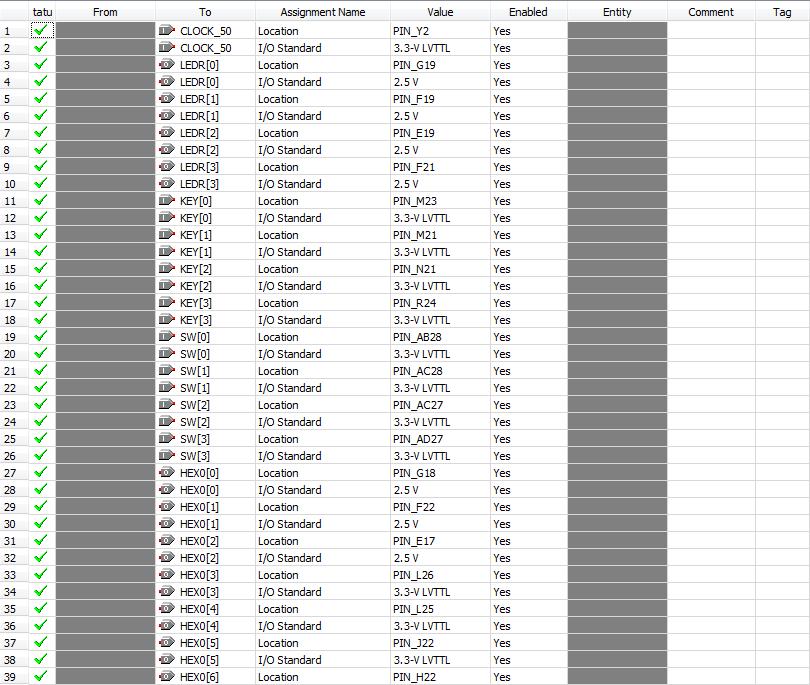
12
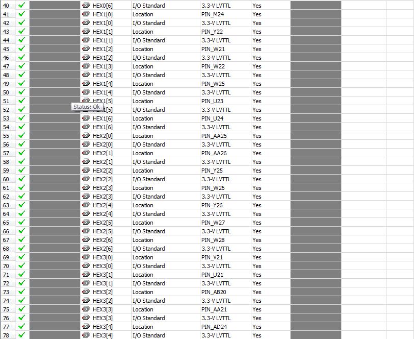
13
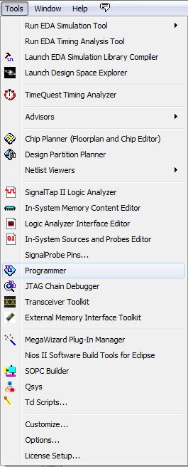
14 Step 6: For any project it is required to create pin assignment from the DE2-115 manual. a) Under Assignments select Assignment Editor b) Add each port under Assignment Name each port will need two assignments: i. PIN location ii. I/O requirement. Note: This process is very lengthy and in the future can be bypassed using System Builder ( PG No. 15). Step 7: When the Verilog code is finished, and all assignments are done, you will be ready to compile your design and program the device.
 Step 9: When it has compiled, double click on Program Device. a) Push the large red button on the FPGA board to turn on the power.")
15 Step 8: At the top of the screen, select the Play button to begin the automatic compilation process. Watch in the lower left screen as the compilation process occurs. This may take several minutes. (Step 7) Step 9: When it has compiled, double click on Program Device. a) Push the large red button on the FPGA board to turn on the power. b) Programmer will open, and at the top left USB Blaster will appear. If it does not, click on Hardware Setup. Select USB Blaster and click ok. c) When USB Blaster appears next to Hardware Setup select Start and watch the upper right corner as the design is implemented. d) When the Progress bar has reach 100% you may test your design on the FPGA board.
16

 Name the project under Project Name: in this Tutorial we name or project Binary_Adder 3) Check all Components that you will be using: in this Tutorial we")
17 System Builder Alternate way to do pin assignments with the help of System Builder System builder is a GUI that creates pin assignment by selecting the components that will be needed for a project. System builder saves time by creating the pin assignments for you and letting you choose what components you need. For Example:- 1) Open DE2_115_tools->DE2_115_system_builder to find DE2_115_SystemBuilder.exe 2) Name the project under Project Name: in this Tutorial we name or project Binary_Adder 3) Check all Components that you will be using: in this Tutorial we are using CLOCK, LEDx27, Buttonx4, 7-Segementx8, Switchx18, and of course the LCD.
 Delete the verilog code that System Builder created then copy the code from Binary_Adder_System_Builder 8) Go")
18 4) Click Generate 5) Create a directory for your project and then click save 6) To open this project open the.qpf file 7) Delete the verilog code that System Builder created then copy the code from Binary_Adder_System_Builder 8) Go to steps 8 and 9


19 7 Segment Hex Display In this project we used four 7-segment displays to show the values of switches being turned on in binary. In a 7- segment display a high logic level will turn off the led and a low logic level to a segment will turn the led on. To represent an LED with a seven-bit value we use the values zero through six. To display a zero to a segment we set the hex value to be equal to
20 7b This is because a zero will have all led on but the center led (number 6 on the figure above). The code also uses a function to simplify the task of representing a bit value to a hex value. Since the function DISPLAYNUMBERS only has one output it seemed like a function instead of a task. In the function we have only one input value that represents a 4 bit switch value, this value is passed through a series of if else statements to determine the hex value. At the end of this program we assign all appropriate values to the represented LEDs. There is a quick example of getting the LED s, Switches, Keys, and 7 segment Hex Display to function properly in the link below that goes more in detail about the 7 segment display.

21 16 x 2 LCD
22 To display characters to an LCD there is a series of steps that need to be done before to initializing the LCD module. Since Verilog doesn t read code sequentially we created a case statement that will allow the initialization to be done in order. This is done by changing the state of the case to the next step in every case statement. The steps performed are RESET1, RESET2, RESET3, FUNCTION SET, DISPLAY OFF, DISPLAY CLEAR, RETURN HOME, CHANGE
23 LINE, DROP LCD, HOLD, DISPLAY ON, and MODE SET AND PRINT STRING. These reset needs to be done three time to because we need to initialize enable to high and register select and read/write to low signals. These steps are also done to communicate with the LCD to determine if it will be an 8 or 4 bit data bus, this is done by setting the data bus equal to the hex value eight(8 h38). Before we can write to the screen we need to clear the LCD display, this is done by changing the data bus equal to 8 h01 (Start of heading). Finally when we need to display the screen we set enable and read/write to high and reset to low, this is done because this allows us to write data to the LCD. In the print string case statement we added an else if (index ==line1) because without this the LCD wouldn t know when the next line begin or the first line starts.
Tutorial for Altera DE1 and Quartus II
 Tutorial for Altera DE1 and Quartus II Qin-Zhong Ye December, 2013 This tutorial teaches you the basic steps to use Quartus II version 13.0 to program Altera s FPGA, Cyclone II EP2C20 on the Development
DKAN0011A Setting Up a Nios II System with SDRAM on the DE2
 DKAN0011A Setting Up a Nios II System with SDRAM on the DE2 04 November 2009 Introduction This tutorial details how to set up and instantiate a Nios II system on Terasic Technologies, Inc. s DE2 Altera
Quick Tutorial for Quartus II & ModelSim Altera
 Quick Tutorial for Quartus II & ModelSim Altera By Ziqiang Patrick Huang Hudson 213c Ziqiang.huang@duke.edu Download & Installation For Windows or Linux users : Download Quartus II Web Edition v13.0 (ModelSim
NIOS CPU Based Embedded Computer System on Programmable Chip
 1 Objectives NIOS CPU Based Embedded Computer System on Programmable Chip EE8205: Embedded Computer Systems This lab has been constructed to introduce the development of dedicated embedded system based
CPE 200L LABORATORY 4: INTRODUCTION TO DE2 BOARD UNIVERSITY OF NEVADA, LAS VEGAS GOALS: BACKGROUND:
 CPE 200L LABORATORY 4: INTRODUCTION TO DE2 BOARD DEPARTMENT OF ELECTRICAL AND COMPUTER ENGINEERING UNIVERSITY OF NEVADA, LAS VEGAS GOALS: Getting familiar with DE2 board installation, properties, usage.
NIOS CPU Based Embedded Computer System on Programmable Chip
 NIOS CPU Based Embedded Computer System on Programmable Chip 1 Lab Objectives EE8205: Embedded Computer Systems NIOS-II SoPC: PART-I This lab has been constructed to introduce the development of dedicated
EE 231 Fall Lab 1: Introduction to Verilog HDL and Altera IDE
 Lab 1: Introduction to Verilog HDL and Altera IDE Introduction In this lab you will design simple circuits by programming the Field-Programmable Gate Array (FPGA). At the end of the lab you should be able
NIOS CPU Based Embedded Computer System on Programmable Chip
 NIOS CPU Based Embedded Computer System on Programmable Chip EE8205: Embedded Computer Systems NIOS-II SoPC: PART-II 1 Introduction This lab has been constructed to introduce the development of dedicated
University of Massachusetts Amherst Computer Systems Lab 2 (ECE 354) Spring Lab 1: Using Nios 2 processor for code execution on FPGA
 Spring Lab 1: Using Nios 2 processor for code execution on FPGA") University of Massachusetts Amherst Computer Systems Lab 2 (ECE 354) Spring 2007 Lab 1: Using Nios 2 processor for code execution on FPGA Objectives: After the completion of this lab: 1. You will understand
University of Massachusetts Amherst Computer Systems Lab 2 (ECE 354) Spring 2007 Lab 1: Using Nios 2 processor for code execution on FPGA Objectives: After the completion of this lab: 1. You will understand
Contents. Appendix B HDL Entry Tutorial 2 Page 1 of 14
 Appendix B HDL Entry Tutorial 2 Page 1 of 14 Contents Appendix B HDL Entry Tutorial 2...2 B.1 Getting Started...2 B.1.1 Preparing a Folder for the Project...2 B.1.2 Starting Quartus II...2 B.1.3 Creating
Chapter 2 Getting Hands on Altera Quartus II Software
 Chapter 2 Getting Hands on Altera Quartus II Software Contents 2.1 Installation of Software... 20 2.2 Setting Up of License... 21 2.3 Creation of First Embedded System Project... 22 2.4 Project Building
ECE 3610 Microprocessing Systems Lab #1 Verilog Design of the TOC Using Quartus II
 ECE 3610 Microprocessing Systems Lab #1 Verilog Design of the TOC Using Quartus II This lab manual presents an introduction to the Quartus II Computer Aided Design (CAD) system. This manual gives step-by-step
NOTE: This tutorial contains many large illustrations. Page breaks have been added to keep images on the same page as the step that they represent.
 CSE 352 Tutorial # 4 Synthesizing onto an FPGA Objectives This tutorial will walk you through the steps of implementing a design made in Active-HDL onto the Altera Cyclone II FPGA NOTE: This tutorial contains
CSE P567 - Winter 2010 Lab 1 Introduction to FGPA CAD Tools
 CSE P567 - Winter 2010 Lab 1 Introduction to FGPA CAD Tools This is a tutorial introduction to the process of designing circuits using a set of modern design tools. While the tools we will be using (Altera
FPGA Introductory Tutorial: Part 1
 FPGA Introductory Tutorial: Part 1 This tutorial is designed to assist in learning the basics of the Altera Quartus II v9.0 software. Part 1 of the tutorial will cover the basics of creating a Project,
Laboratory Exercise 8
 Laboratory Exercise 8 Memory Blocks In computer systems it is necessary to provide a substantial amount of memory. If a system is implemented using FPGA technology it is possible to provide some amount
SOPC LAB1. I. Introduction. II. Lab contents. 4-bit count up counter. Advanced VLSI Due Wednesday, 01/08/2003
 SOPC LAB1 I. Introduction The purpose of this lab is to familiarize you with all the items in the kit. This tutorial tells you how to develop FPGA system in Quartus II. You are ready to begin using the
Tutorial on Quartus II Introduction Using Verilog Code
 Tutorial on Quartus II Introduction Using Verilog Code (Version 15) 1 Introduction This tutorial presents an introduction to the Quartus II CAD system. It gives a general overview of a typical CAD flow
EE 231 Fall EE 231 Lab 2
 EE 231 Lab 2 Introduction to Verilog HDL and Quartus In the previous lab you designed simple circuits using discrete chips. In this lab you will do the same but by programming the CPLD. At the end of the
Lab 2 EECE473 Computer Organization & Architecture University of Maine
 Lab 2: Verilog Programming Instructor: Yifeng Zhu 50 Points Objectives: 1. Quatus II Programming assignment: PIN assignments, LEDs, switches; 2. Download and test the design on Altera DE2 board 3. Create
Introduction to the Altera SOPC Builder Using Verilog Designs. 1 Introduction
 Introduction to the Altera SOPC Builder Using Verilog Designs 1 Introduction This tutorial presents an introduction to Altera s SOPC Builder software, which is used to implement a system that uses the
2 nd Year Laboratory. Experiment: FPGA Design with Verilog. Department of Electrical & Electronic Engineering. Imperial College London.
 Department of Electrical & Electronic Engineering 2 nd Year Laboratory Experiment: FPGA Design with Verilog Objectives By the end of this experiment, you should know: How to design digital circuits using
PREFACE. Changes to the SOPC Edition
 PREFACE Changes to the SOPC Edition Rapid Prototyping of Digital Systems provides an exciting and challenging laboratory component for undergraduate digital logic and computer design courses using FPGAs
Lab 6: Integrated the Decoder with Muti-bit Counter and Programming a FPGA
 Lab 6: Integrated the Decoder with Muti-bit Counter and Programming a FPGA For your report: The problem written in English The flowchart or function table to solve the problem if it is necessary The design
Tutorial on Quartus II Introduction Using Schematic Designs
 Tutorial on Quartus II Introduction Using Schematic Designs (Version 15) 1 Introduction This tutorial presents an introduction to the Quartus II CAD system. It gives a general overview of a typical CAD
QUARTUS II Altera Corporation
 QUARTUS II Quartus II Design Flow Design Entry Timing Constraints Synthesis Placement and Routing Timing, Area, Power Optimization Timing and Power Analyzer Optimized Design 2 Can I still use a Processor?
Introduction to the Altera SOPC Builder Using Verilog Design
 Introduction to the Altera SOPC Builder Using Verilog Design This tutorial presents an introduction to Altera s SOPC Builder software, which is used to implement a system that uses the Nios II processor
SignalTap II with Verilog Designs. 1 Introduction. For Quartus II 13.1
 SignalTap II with Verilog Designs For Quartus II 13.1 1 Introduction This tutorial explains how to use the SignalTap II feature within Altera s Quartus II software. The SignalTap II Embedded Logic Analyzer
Experiment 18 Full Adder and Parallel Binary Adder
 Objectives Experiment 18 Full Adder and Parallel Binary Adder Upon completion of this laboratory exercise, you should be able to: Create and simulate a full adder in VHDL, assign pins to the design, and
Quartus II Introduction Using Verilog Design
 Quartus II Introduction Using Verilog Design This tutorial presents an introduction to the Quartus R II CAD system. It gives a general overview of a typical CAD flow for designing circuits that are implemented
PHYS 623 Field Programmable Gate Arrays Laboratory 1
 PHYS 623 Field Programmable Gate Arrays Laboratory 1 Ian Wisher, University of Wisconsin Physics Department Last edits October 19, 2015 1 Primer In this lab we will explore one of the most exciting developments
Debugging Nios II Systems with the SignalTap II Logic Analyzer
 Debugging Nios II Systems with the SignalTap II Logic Analyzer May 2007, ver. 1.0 Application Note 446 Introduction As FPGA system designs become more sophisticated and system focused, with increasing
EMT1250 LABORATORY EXPERIMENT. EXPERIMENT # 6: Quartus II Tutorial and Practice. Name: Date:
 EXPERIMENT # 6: Quartus II Tutorial and Practice Name: Date: Equipment/Parts Needed: Quartus II R Web Edition V9.1 SP2 software by Altera Corporation USB drive to save your files Objective: Learn how to
FPGA RGB Matrix. Created by lady ada. Last updated on :15:42 PM UTC
 FPGA RGB Matrix Created by lady ada Last updated on 2017-12-27 09:15:42 PM UTC Guide Contents Guide Contents Overview Controlling the Adafruit 32x16 RGB LED Matrix with a DE0-Nano FPGA Board Prerequisites
University of Florida EEL 3701 Dr. Eric M. Schwartz Madison Emas, TA Department of Electrical & Computer Engineering Revision 1 5-Jun-17
 Page 1/14 Example Problem Given the logic equation Y = A*/B + /C, implement this equation using a two input AND gate, a two input OR gate and two inverters under the Quartus environment. Upon completion
ECE 437 Computer Architecture and Organization Lab 6: Programming RAM and ROM Due: Thursday, November 3
 Objectives: ECE 437 Computer Architecture and Organization Lab 6: Programming RAM and ROM Due: Thursday, November 3 Build Instruction Memory and Data Memory What to hand in: Your implementation source
Digital Systems Laboratory
 2012 Fall CSE140L Digital Systems Laboratory by Dr. Choon Kim CSE Department UCSD 1 Welcome to CSE140L! 2 3-way Light Controller, 2-1 MUX, Majority Detector, 7- seg Display, Binary-to- Decimal converter.
Laboratory 4 Design a Muti-bit Counter and Programming a FPGA
 Laboratory 4 Design a Muti-bit Counter and Programming a FPGA For your report: The problem written in English The flowchart or function table to solve the problem if it is necessary The design entry included
E85: Digital Design and Computer Engineering Lab 2: FPGA Tools and Combinatorial Logic Design
 E85: Digital Design and Computer Engineering Lab 2: FPGA Tools and Combinatorial Logic Design Objective The purpose of this lab is to learn to use Field Programmable Gate Array (FPGA) tools to simulate
EXPERIMENT 1. INTRODUCTION TO ALTERA
 EXPERIMENT 1. INTRODUCTION TO ALTERA I. Introduction I.I Objectives In this experiment, you will learn computer aided digital design and verification of it using Field Programmable Gate Arrays (FPGA).
Building Combinatorial Circuit Using Behavioral Modeling Lab
 Building Combinatorial Circuit Using Behavioral Modeling Lab Overview: In this lab you will learn how to model a combinatorial circuit using behavioral modeling style of Verilog HDL. You will model a combinatorial
Quartus II Introduction Using Schematic Design
 Quartus II Introduction Using Schematic Design This tutorial presents an introduction to the Quartus R II CAD system. It gives a general overview of a typical CAD flow for designing circuits that are implemented
Chip Design with FPGA Design Tools
 Chip Design with FPGA Design Tools Intern: Supervisor: Antoine Vazquez Janusz Zalewski Florida Gulf Coast University Fort Myers, FL 33928 V1.9, August 28 th. Page 1 1. Introduction FPGA is abbreviation
University of Massachusetts Amherst Computer Systems Lab 1 (ECE 354) LAB 1 Reference Manual
 LAB 1 Reference Manual") University of Massachusetts Amherst Computer Systems Lab 1 (ECE 354) LAB 1 Reference Manual Lab 1: Using NIOS II processor for code execution on FPGA Objectives: 1. Understand the typical design flow in
University of Massachusetts Amherst Computer Systems Lab 1 (ECE 354) LAB 1 Reference Manual Lab 1: Using NIOS II processor for code execution on FPGA Objectives: 1. Understand the typical design flow in
EMBEDDED SOPC DESIGN WITH NIOS II PROCESSOR AND VHDL EXAMPLES
 EMBEDDED SOPC DESIGN WITH NIOS II PROCESSOR AND VHDL EXAMPLES Pong P. Chu Cleveland State University A JOHN WILEY & SONS, INC., PUBLICATION PREFACE An SoC (system on a chip) integrates a processor, memory
Laboratory Exercise 3 Comparative Analysis of Hardware and Emulation Forms of Signed 32-Bit Multiplication
 Laboratory Exercise 3 Comparative Analysis of Hardware and Emulation Forms of Signed 32-Bit Multiplication Introduction All processors offer some form of instructions to add, subtract, and manipulate data.
Tutorial 2 Implementing Circuits in Altera Devices
 Appendix C Tutorial 2 Implementing Circuits in Altera Devices In this tutorial we describe how to use the physical design tools in Quartus II. In addition to the modules used in Tutorial 1, the following
CHAPTER 1 INTRODUCTION... 1 CHAPTER 2 ASSIGN THE DEVICE... 7 CHAPTER 3 DESIGN ENTRY CHAPTER 4 COMPILE AND VERIFY YOUR DESIGN...
 CONTENTS CHAPTER 1 INTRODUCTION... 1 1.1 DESIGN FLOW... 1 1.2 BEFORE YOU BEGIN... 2 1.3 WHAT YOU WILL LEARN... 6 CHAPTER 2 ASSIGN THE DEVICE... 7 2.1 ASSIGN THE DEVICE... 7 CHAPTER 3 DESIGN ENTRY... 11
EMT1250 LABORATORY EXPERIMENT. EXPERIMENT # 7: VHDL and DE2 Board. Name: Date:
 EXPERIMENT # 7: VHDL and DE2 Board Name: Date: Equipment/Parts Needed: Quartus II R Web Edition V9.1 SP2 software by Altera Corporation USB drive to save your files Objective: Learn how to create and modify
IMPLEMENTING COUNTERS
 EECS:6660:0xxField Programmable Gate Arrays s11l1_fpga.fm - 1 Lab Assignment #1 Due Thursday, March 31 2011 IMPLEMENTING COUNTERS 1. OBJECTIVES - learning the VHDL implementation process using Language
Terasic DE0 Field Programmable Gate Array (FPGA) Development Board
 Development Board") Lecture FPGA-01 DE0 FPGA Development Board and Quartus II 9.1 FPGA Design Software Terasic DE0 Field Programmable Gate Array (FPGA) Development Board 1 May 16, 2013 3 Layout and Components of DE0 May 16,
Lecture FPGA-01 DE0 FPGA Development Board and Quartus II 9.1 FPGA Design Software Terasic DE0 Field Programmable Gate Array (FPGA) Development Board 1 May 16, 2013 3 Layout and Components of DE0 May 16,
Quartus II Version 14.0 Tutorial Created September 10, 2014; Last Updated January 9, 2017
 Quartus II Version 14.0 Tutorial Created September 10, 2014; Last Updated January 9, 2017 This tutorial will walk you through the process of developing circuit designs within Quartus II, simulating with
Quartus II Introduction Using Verilog Designs. 1 Introduction. For Quartus II 12.0
 Quartus II Introduction Using Verilog Designs For Quartus II 12.0 1 Introduction This tutorial presents an introduction to the Quartus II CAD system. It gives a general overview of a typical CAD flow for
CSCB58 - Lab 0. Intro to The Lab & The DE2 Board. Prelab /4 Part I (in-lab) /1 Part II (in-lab) /1
 /1 Part II (in-lab) /1") CSCB58 - Lab 0 Intro to The Lab & The DE2 Board Learning Objectives This week we will be getting you familiar with the lab and the boards that we will be using in later labs. You will also learn how to
CSCB58 - Lab 0 Intro to The Lab & The DE2 Board Learning Objectives This week we will be getting you familiar with the lab and the boards that we will be using in later labs. You will also learn how to
Lab 2: Introduction to Verilog HDL and Quartus
 Lab 2: Introduction to Verilog HDL and Quartus September 16, 2008 In the previous lab you designed simple circuits using discrete chips. In this lab you will do the same but by programming the CPLD. At
Tutorial 3. Appendix D. D.1 Design Using Verilog Code. The Ripple-Carry Adder Code. Functional Simulation
 Appendix D Tutorial 3 This tutorial introduces more advanced capabilities of the Quartus II system. We show how Verilog code is organized and compiled and illustrate how multibit signals are represented
Making Qsys Components. 1 Introduction. For Quartus II 13.0
 Making Qsys Components For Quartus II 13.0 1 Introduction The Altera Qsys tool allows a digital system to be designed by interconnecting selected Qsys components, such as processors, memory controllers,
TLL5000 Electronic System Design Base Module. Getting Started Guide, Ver 3.4
 TLL5000 Electronic System Design Base Module Getting Started Guide, Ver 3.4 COPYRIGHT NOTICE The Learning Labs, Inc. ( TLL ) All rights reserved, 2008 Reproduction in any form without permission is prohibited.
UNIVERSITY OF CALIFORNIA, DAVIS Department of Electrical and Computer Engineering. EEC180A DIGITAL SYSTEMS I Winter 2015
 UNIVERSITY OF CALIFORNIA, DAVIS Department of Electrical and Computer Engineering EEC180A DIGITAL SYSTEMS I Winter 2015 LAB 1: Introduction to Quartus II Schematic Capture and ModelSim Simulation This
Xilinx ChipScope ICON/VIO/ILA Tutorial
 Xilinx ChipScope ICON/VIO/ILA Tutorial The Xilinx ChipScope tools package has several modules that you can add to your Verilog design to capture input and output directly from the FPGA hardware. These
Verilog Design Entry, Synthesis, and Behavioral Simulation
 ------------------------------------------------------------- PURPOSE - This lab will present a brief overview of a typical design flow and then will start to walk you through some typical tasks and familiarize
Quartus II Tutorial. September 10, 2014 Quartus II Version 14.0
 Quartus II Tutorial September 10, 2014 Quartus II Version 14.0 This tutorial will walk you through the process of developing circuit designs within Quartus II, simulating with Modelsim, and downloading
Altera Technical Training Quartus II Software Design
 Altera Technical Training Quartus II Software Design Exercises Quartus II Software Design Series: Foundation 2 Quartus II Software Design Series: Foundation Exercises Exercise 1 3 Exercises Quartus II
Laboratory 4 Design a Muti-bit Counter
 Laboratory 4 Design a Muti-bit Counter Background A. Approach I: Design 3-bit counter with and clear T-type flip-flop is shown in Figure 1. A T flip-flop is obtained from a JK flip-flop by tying the J
HyperBus Memory Controller (HBMC) Tutorial
 Tutorial") Synaptic Labs' HyperBus Memory Controller (HBMC) Tutorial T001A: A Qsys based Nios II Reference design with a simple self test of the HyperFlash and HyperRAM device using S/Labs' HBMC IP This tutorial
Synaptic Labs' HyperBus Memory Controller (HBMC) Tutorial T001A: A Qsys based Nios II Reference design with a simple self test of the HyperFlash and HyperRAM device using S/Labs' HBMC IP This tutorial
Banks, Jasmine Elizabeth (2011) The Spartan 3E Tutorial 1 : Introduction to FPGA Programming, Version 1.0. [Tutorial Programme]
![Banks, Jasmine Elizabeth (2011) The Spartan 3E Tutorial 1 : Introduction to FPGA Programming, Version 1.0. [Tutorial Programme]](/thumbs/75/72381729.jpg "Banks, Jasmine Elizabeth (2011) The Spartan 3E Tutorial 1 : Introduction to FPGA Programming, Version 1.0. [Tutorial Programme]") QUT Digital Repository: http://eprints.qut.edu.au/ This is the author version published as: This is the accepted version of this article. To be published as : This is the author s version published as:
QUT Digital Repository: http://eprints.qut.edu.au/ This is the author version published as: This is the accepted version of this article. To be published as : This is the author s version published as:
Quartus II Tutorial. September 10, 2014 Quartus II Version 14.0
 Quartus II Tutorial September 10, 2014 Quartus II Version 14.0 This tutorial will walk you through the process of developing circuit designs within Quartus II, simulating with Modelsim, and downloading
1 Introduction 2. 2 Background 3. 3 Getting Started 4. 4 Starting a New Project 6. 5 Design Entry Using VHDL Code 13
 Quartus Prime Introduction Using VHDL Designs For Quartus Prime 17.0 Contents 1 Introduction 2 2 Background 3 3 Getting Started 4 3.1 Quartus Prime Online Help................................................................................................
Laboratory Exercise 1
 Laboratory Exercise 1 Switches, Lights, and Multiplexers The purpose of this exercise is to learn how to connect simple input and output devices to an FPGA chip and implement a circuit that uses these
UNIVERSITI MALAYSIA PERLIS
 UNIVERSITI MALAYSIA PERLIS SCHOOL OF COMPUTER & COMMUNICATIONS ENGINEERING EKT 124 LABORATORY MODULE INTRODUCTION TO QUARTUS II DESIGN SOFTWARE : INTRODUCTION TO QUARTUS II DESIGN SOFTWARE OBJECTIVES To
Using Library Modules in Verilog Designs. 1 Introduction. For Quartus II 13.0
 Using Library Modules in Verilog Designs For Quartus II 13.0 1 Introduction This tutorial explains how Altera s library modules can be included in Verilog-based designs, which are implemented by using
DDR and DDR2 SDRAM Controller Compiler User Guide
 DDR and DDR2 SDRAM Controller Compiler User Guide 101 Innovation Drive San Jose, CA 95134 www.altera.com Operations Part Number Compiler Version: 8.1 Document Date: November 2008 Copyright 2008 Altera
Error Correction Code (ALTECC_ENCODER and ALTECC_DECODER) Megafunctions User Guide
 Megafunctions User Guide") Error Correction Code (ALTECC_ENCODER and ALTECC_DECODER) Megafunctions User Guide 11 Innovation Drive San Jose, CA 95134 www.altera.com Software Version 8. Document Version: 2. Document Date: June 28
Error Correction Code (ALTECC_ENCODER and ALTECC_DECODER) Megafunctions User Guide 11 Innovation Drive San Jose, CA 95134 www.altera.com Software Version 8. Document Version: 2. Document Date: June 28
TLL5000 Electronic System Design Base Module
 TLL5000 Electronic System Design Base Module The Learning Labs, Inc. Copyright 2007 Manual Revision 2007.12.28 1 Copyright 2007 The Learning Labs, Inc. Copyright Notice The Learning Labs, Inc. ( TLL )
ECE 4305 Computer Architecture Lab #1
 ECE 4305 Computer Architecture Lab #1 The objective of this lab is for students to familiarize with the FPGA prototyping system board (Nexys-2) and the Xilinx software development environment that will
HyperBus Memory Controller (HBMC) Tutorial
 Tutorial") Synaptic Labs' HyperBus Memory Controller (HBMC) Tutorial T005B: A Qsys based Nios II Reference design with a simple application running from HyperFlash and HyperRAM device using S/Labs' HBMC IP. The HyperRAM
Synaptic Labs' HyperBus Memory Controller (HBMC) Tutorial T005B: A Qsys based Nios II Reference design with a simple application running from HyperFlash and HyperRAM device using S/Labs' HBMC IP. The HyperRAM
VHDL for Synthesis. Course Description. Course Duration. Goals
 VHDL for Synthesis Course Description This course provides all necessary theoretical and practical know how to write an efficient synthesizable HDL code through VHDL standard language. The course goes
My First FPGA Design Tutorial
 101 Innovation Drive San Jose, CA 95134 (408) 544-7000 http://www.altera.com TU-01002-1.0 Copyright 2007 Altera Corporation. All rights reserved. Altera, The Programmable Solutions Company, the stylized
Configuration and programming minimodules MMfpga01 and MMfpga11
 MMfpga01 MMfpga11 Configuration and programming minimodules MMfpga01 and MMfpga11 1 Index 1. Instalation of the QUARTUS II Web Edition...3 2. How to install QUARTUS II Web Edition...5 3. Installation of
TESTING ON THE DE2 BOARD
 TESTING ON THE DE2 BOARD September 18 th, 2007 CSC343 Fall 2007 Prepared by: Steven Medina PURPOSE The DE2 board is a programmable board with an FPGA chip attached. FPGA stands for Field Programmable Gate
CET4805 Component and Subsystem Design II. EXPERIMENT # 5: Adders. Name: Date:
 EXPERIMENT # 5: Adders Name: Date: Equipment/Parts Needed: Quartus II R Web Edition V9.1 SP2 software by Altera Corporation USB drive to save your files Objective: Design a half adder by extracting the
Introduction to Simulation of VHDL Designs Using ModelSim Graphical Waveform Editor. 1 Introduction. For Quartus Prime 16.1
 Introduction to Simulation of VHDL Designs Using ModelSim Graphical Waveform Editor For Quartus Prime 16.1 1 Introduction This tutorial provides an introduction to simulation of logic circuits using the
ECSE-323 Digital System Design. Lab #1 Using the Altera Quartus II Software Fall 2008
 1 ECSE-323 Digital System Design Lab #1 Using the Altera Quartus II Software Fall 2008 2 Introduction. In this lab you will learn the basics of the Altera Quartus II FPGA design software through following
Laboratory Exercise 7
 Laboratory Exercise 7 Finite State Machines This is an exercise in using finite state machines. Part I We wish to implement a finite state machine (FSM) that recognizes two specific sequences of applied
The development board used in this class is ALTERA s DE The board provides the following hardware:
 Lab 1 The goal of this lab is to get familiar with the mechanics of designing digital systems using VHDL and ALTERA s FPGAs. The development board used in this class is ALTERA s DE2-115. The board provides
My First FPGA for Altera DE2-115 Board
 My First FPGA for Altera DE2-115 Board 數位電路實驗 TA: 吳柏辰 Author: Trumen Outline Complete Your Verilog Design Assign The Device Add a PLL Megafunction Assign the Pins Create a Default TimeQuest SDC File Compile
Using the Serial FlashLoader With the Quartus II Software
 Using the Serial FlashLoader With the Quartus II Software July 2006, ver. 3.0 Application Note 370 Introduction Using the Joint Test Action Group () interface, the Altera Serial FlashLoader (SFL) is the
Verilog for High Performance
 Verilog for High Performance Course Description This course provides all necessary theoretical and practical know-how to write synthesizable HDL code through Verilog standard language. The course goes
HyperBus Memory Controller (HBMC) Tutorial
 Tutorial") Synaptic Labs' HyperBus Memory Controller (HBMC) Tutorial T005C: A Qsys based Nios II Reference design with a simple HyperFlash test device using S/Labs' HBMC IP and S/Labs' Memory Region Mapper IP This
Synaptic Labs' HyperBus Memory Controller (HBMC) Tutorial T005C: A Qsys based Nios II Reference design with a simple HyperFlash test device using S/Labs' HBMC IP and S/Labs' Memory Region Mapper IP This
CSEE W4840 Embedded System Design Lab 1
 CSEE W4840 Embedded System Design Lab 1 Stephen A. Edwards Due January 31, 2008 Abstract Learn to use the Altera Quartus development envrionment and the DE2 boards by implementing a small hardware design
University of Florida EEL 3701 Dr. Eric M. Schwartz Department of Electrical & Computer Engineering Revision 0 12-Jun-16
 Page 1/14 Quartus Tutorial with Basic Graphical Gate Entry and Simulation Example Problem Given the logic equation Y = A*/B + /C, implement this equation using a two input AND gate, a two input OR gate
POS-PHY Level 2 and 3 Compiler User Guide
 POS-PHY Level 2 and 3 Compiler User Guide 101 Innovation Drive San Jose, CA 95134 www.altera.com MegaCore Version: 8.1 Document Date: November 2008 Copyright 2008 Altera Corporation. All rights reserved.
Name EGR 2131 Lab #6 Number Representation and Arithmetic Circuits
 Name EGR 2131 Lab #6 Number Representation and Arithmetic Circuits Equipment and Components Quartus software and Altera DE2-115 board PART 1: Number Representation in Microsoft Calculator. First, let s
Xilinx Tutorial Basic Walk-through
 Introduction to Digital Logic Design with FPGA s: Digital logic circuits form the basis of all digital electronic devices. FPGAs (Field Programmable Gate Array) are large programmable digital electronic
HyperBus Memory Controller (HBMC) Tutorial
 Tutorial") Synaptic Labs' HyperBus Memory Controller (HBMC) Tutorial T002A: A Qsys based Nios II reference design using Intel s MSGDMA to benchmark memory copy operations on the HyperRAM device using S/Labs' HBMC
Synaptic Labs' HyperBus Memory Controller (HBMC) Tutorial T002A: A Qsys based Nios II reference design using Intel s MSGDMA to benchmark memory copy operations on the HyperRAM device using S/Labs' HBMC
Experiment 3 Introduction to Verilog Programming using Quartus II software Prepared by: Eng. Shatha Awawdeh, Eng.Eman Abu_Zaitoun
 Experiment 3 Introduction to Verilog Programming using Quartus II software Prepared by: Eng. Shatha Awawdeh, Eng.Eman Abu_Zaitoun Introduction: Verilog HDL is a hardware description language used to design
EXPERIMENT NUMBER 7 HIERARCHICAL DESIGN OF A FOUR BIT ADDER (EDA-2)
") 7-1 EXPERIMENT NUMBER 7 HIERARCHICAL DESIGN OF A FOUR BIT ADDER (EDA-2) Purpose The purpose of this exercise is to explore more advanced features of schematic based design. In particular you will go through
7-1 EXPERIMENT NUMBER 7 HIERARCHICAL DESIGN OF A FOUR BIT ADDER (EDA-2) Purpose The purpose of this exercise is to explore more advanced features of schematic based design. In particular you will go through
DE2 Board & Quartus II Software
 January 23, 2015 Contact and Office Hours Teaching Assistant (TA) Sergio Contreras Office Office Hours Email SEB 3259 Tuesday & Thursday 12:30-2:00 PM Wednesday 1:30-3:30 PM contre47@nevada.unlv.edu Syllabus
Using ModelSim to Simulate Logic Circuits for Altera FPGA Devices
 Using ModelSim to Simulate Logic Circuits for Altera FPGA Devices This tutorial is a basic introduction to ModelSim, a Mentor Graphics simulation tool for logic circuits. We show how to perform functional