ECE 331: N0. Professor Andrew Mason Michigan State University. Opening Remarks
|
|
|
- Brian Spencer
- 6 years ago
- Views:
Transcription


1 ECE 331: N0 ECE230 Review Professor Andrew Mason Michigan State University Spring Announcements Opening Remarks HW1 due next Mon Labs begin in week 4 No class next-next Mon MLK Day ECE230 Review HO_0 posted on web Anyone need a syllabus? Today s Objectives Questions? Perform number base conversions for Dec, Hex, Bin Identify value range as function of number of bits; identify out of range overflow for signed and unsigned binary numbers Express numbers in signed 2 s complement (S2C) form, perform 2 s complement operation, and evaluate subtraction using S2C. Identify value range in S2C and determine 2C overflow Perform minimization of logic expressions using min/max terms, K-maps, and Boolean arithmetic 1.2


2 Be neat! Homework Guidelines should represent a professional work product Show work Clearly indicate answers Give units in answer Grading effort more than results may not be corrected but solutions will be posted Homework Questions come to office hours! 1.3 Digital Bases Decimal (Dec), base 10 Binary (Bin), base 2 Hexadecimal (Hex), base 16 Base Conversions Bin Dec Number Systems Hex Dec Bin Hex TPS: Convert to hex. 1.4
3 Binary Addition DEMO: using PC Calculator to check conversions & math only for checking answers! always show work in homework Addition Examples Decimal Binary Hex Decimal Binary Hex B ] Value Range n unsigned binary bits can only express values 0 to 2 n -1 n unsigned hex bit express values 0 to 16 n -1 larger values generate overflow carry_out bit 1.5 Binary Subtraction Microprocessors do not subtract, they only add! 2 s Complement = 2C X-Y = X+(-Y) = X+[Y]*, where [ ]* means 2 s complement read extensive notes in HO_0a To subtract use numbers in signed 2 s complement (S2C) form use 2C operation to negate subtracted/negative values then ADD EX: Evaluate 5 3 using 4-bit S2C # s value = 2 sign bit 0 = + (positive) carry_out, ignore for subtraction 1.6
4 2 s Complement Overflow EX: Evaluate -7 6 using 4-bit S2C # s value = 3 sign bit 0 = + (positive) carry_out, ignore for subtraction but does -7 6 = 3? No! should = is out of range for 4-bit S2C # 2 s Complement m Overflow: when result of arithmetic is outside the value range of n-bit signed binary number Signed binary range: -2 n-1 to 2 n-1-1 Detecting 2C Overflow: only overflow if sign of both numbers is same & is opposite sign of addition result Overflow A B S A B S n 1 n 1 n 1 n 1 n 1 n Arithmetic with 2C Overflow EX: Evaluate using 3-bit S2C # s, detect 2C overflow 2C Overflow? sign of both #s (at addition) = 0 sign of result = 1 (opposite of 0) 2C overflow! More examples in HO_0a 1.8
5 Bin/Hex Math Examples EX: Evaluate using 4-bit S2C # s, detect 2C overflow meets conditions for 2C overflow, so answer is not reliable EX: Evaluate using 4-bit S2C # s, check answer 1.9 Logic Minimization Often need to reduce a complex logic expression to it smallest form (i.e., fewest number of logic operations) Methods of logic minimization Boolean arithmetic using Boolean properties EX F X Y Z X Y Z X Y Z Z X Y Karnaugh maps EX: Find the minimal SoP expression for XY F (1,2,5,7 ) XYZ Z 0 m 2 1 m 1 m 7 m 5 then reduce using Boolean arithmetic F = XZ + Y Z +X YZ =Z(X+Y ) Z(X+Y +X YZ is the minimal form. 1.10
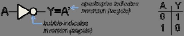
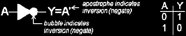
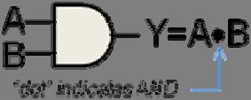
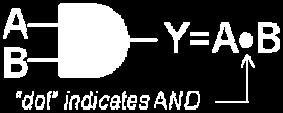
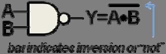
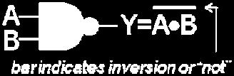
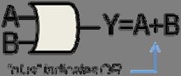
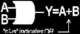
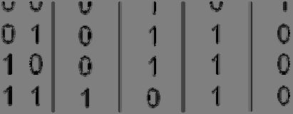
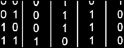
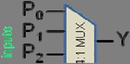
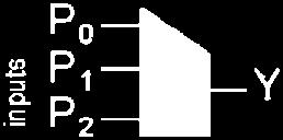
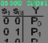
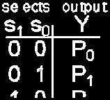
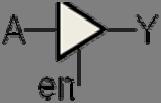
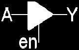
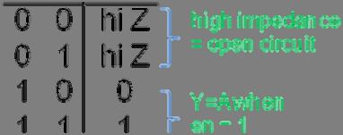
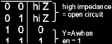
6 Basic Combinational Logic Gates INV AND NAND OR NOR inversion bubbles bbl 1.11 More Combinational Logic MUX: select 1 from many example 4:1 MUX Buffer: signal isolation & drive inverter without the inversion Tri-State (buffer/inverter) buffer (or inverter) with disable (high impedance) state 1.12


 or")
")


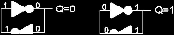
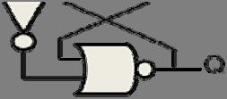
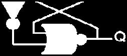
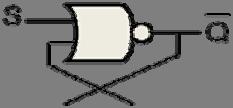
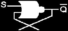
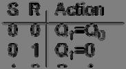
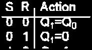
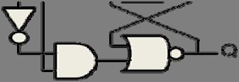
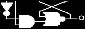
7 XOR & XNOR And More true of both different (XOR) or both same (XNOR) Decoder only one active output example 4:1 decoder difference from MUX? active low concept 1.13 Sequential logic Sequential Logic & Latch difference from combinational? - output based on input value at prior time Latch 2-state storage circuit can hold data bi-stable circuit D-type latch D-type latch w/ enable SR latch 1.14


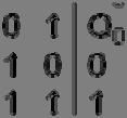
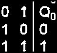
8 Flip Flop Flip flop is a synchronous circuit which means? D-type master-slave slave flip flop latch level logic gate level JK flip flop Toggle flip flop Convertability State tables for D-type type, JK, and T-type flip flops 1.15 Flip Flop Timing Diagrams Timing diagram: map of digital output (& input) vs. time use state table to find output look at proper clock transition ignore input changes outside clock transitions Rising- vs. falling-edge triggered triggered by clock rising = positive = up falling = negative = down CLK D Qp Qn 1.16
9 Data registers Registers stores block (byte/word) of digital data composed of flip flops; used as static memory example: 4b parallel-in parallel-out register Shift register can move data laterally between register bits can input or output (or both) data serially example: 4b serial-in parallel out shift register 1.17 Shift Shift & Rotate move each bit (left or right) to adjacent register, load in preset value (normally 0) into open registers Rotate move each bit (left or right) to adjacent register, rotate exiting bits back into other side of register Example: shift right by 2 rotate left by


 2")
 Example:")

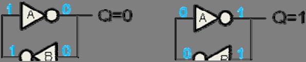
10 DeMorgans & Complete Set DeMorgans Relations Complete Set Concept all logic functions can be implemented with ONLY NAND (or ONLY NOR) example: INV with NAND similarly, can make AND, OR, NOR with only NAND 1.19 Logic Schematic Manipulation Bubble pushing technique bubbles can be moved from input of a gate to the output of an attached gate (or from output to input) 2 bubbles can be added to any node (like double negative) Example: convert to all NANDs ND using DeMorgans & bubble pushing initial F bubble pushing DeMorgans final 1.20
KING FAHD UNIVERSITY OF PETROLEUM & MINERALS COMPUTER ENGINEERING DEPARTMENT
 KING FAHD UNIVERSITY OF PETROLEUM & MINERALS COMPUTER ENGINEERING DEPARTMENT COE 202: Digital Logic Design Term 162 (Spring 2017) Instructor: Dr. Abdulaziz Barnawi Class time: U.T.R.: 11:00-11:50AM Class
BUILDING BLOCKS OF A BASIC MICROPROCESSOR. Part 1 PowerPoint Format of Lecture 3 of Book
 BUILDING BLOCKS OF A BASIC MICROPROCESSOR Part PowerPoint Format of Lecture 3 of Book Decoder Tri-state device Full adder, full subtractor Arithmetic Logic Unit (ALU) Memories Example showing how to write
LECTURE 4. Logic Design
 LECTURE 4 Logic Design LOGIC DESIGN The language of the machine is binary that is, sequences of 1 s and 0 s. But why? At the hardware level, computers are streams of signals. These signals only have two
Final Exam Solution Sunday, December 15, 10:05-12:05 PM
 Last (family) name: First (given) name: Student I.D. #: Circle section: Kim Hu Department of Electrical and Computer Engineering University of Wisconsin - Madison ECE/CS 352 Digital System Fundamentals
Systems Programming. Lecture 2 Review of Computer Architecture I
 Systems Programming www.atomicrhubarb.com/systems Lecture 2 Review of Computer Architecture I In The Book Patt & Patel Chapter 1,2,3 (review) Outline Binary Bit Numbering Logical operations 2's complement
END-TERM EXAMINATION
 (Please Write your Exam Roll No. immediately) END-TERM EXAMINATION DECEMBER 2006 Exam. Roll No... Exam Series code: 100919DEC06200963 Paper Code: MCA-103 Subject: Digital Electronics Time: 3 Hours Maximum
1. Prove that if you have tri-state buffers and inverters, you can build any combinational logic circuit. [4]
![1. Prove that if you have tri-state buffers and inverters, you can build any combinational logic circuit. [4]](/thumbs/81/83055464.jpg "1. Prove that if you have tri-state buffers and inverters, you can build any combinational logic circuit. [4]") HW 3 Answer Key 1. Prove that if you have tri-state buffers and inverters, you can build any combinational logic circuit. [4] You can build a NAND gate from tri-state buffers and inverters and thus you
HW 3 Answer Key 1. Prove that if you have tri-state buffers and inverters, you can build any combinational logic circuit. [4] You can build a NAND gate from tri-state buffers and inverters and thus you
Code No: R Set No. 1
 Code No: R059210504 Set No. 1 II B.Tech I Semester Regular Examinations, November 2007 DIGITAL LOGIC DESIGN ( Common to Computer Science & Engineering, Information Technology and Computer Science & Systems
Code No: R Set No. 1
 Code No: R059210504 Set No. 1 II B.Tech I Semester Supplementary Examinations, February 2007 DIGITAL LOGIC DESIGN ( Common to Computer Science & Engineering, Information Technology and Computer Science
SUBJECT CODE: IT T35 DIGITAL SYSTEM DESIGN YEAR / SEM : 2 / 3
 UNIT - I PART A (2 Marks) 1. Using Demorgan s theorem convert the following Boolean expression to an equivalent expression that has only OR and complement operations. Show the function can be implemented
Injntu.com Injntu.com Injntu.com R16
 1. a) What are the three methods of obtaining the 2 s complement of a given binary (3M) number? b) What do you mean by K-map? Name it advantages and disadvantages. (3M) c) Distinguish between a half-adder
Question Total Possible Test Score Total 100
 Computer Engineering 2210 Final Name 11 problems, 100 points. Closed books, closed notes, no calculators. You would be wise to read all problems before beginning, note point values and difficulty of problems,
Philadelphia University Student Name: Student Number:
 Philadelphia University Student Name: Student Number: Faculty of Engineering Serial Number: Final Exam, First Semester: 2018/2019 Dept. of Computer Engineering Course Title: Logic Circuits Date: 03/01/2019
R10. II B. Tech I Semester, Supplementary Examinations, May
 SET - 1 1. a) Convert the following decimal numbers into an equivalent binary numbers. i) 53.625 ii) 4097.188 iii) 167 iv) 0.4475 b) Add the following numbers using 2 s complement method. i) -48 and +31
II/IV B.Tech (Regular/Supplementary) DEGREE EXAMINATION. Answer ONE question from each unit.
 DEGREE EXAMINATION. Answer ONE question from each unit.") Hall Ticket Number: 14CS IT303 November, 2017 Third Semester Time: Three Hours Answer Question No.1 compulsorily. II/IV B.Tech (Regular/Supplementary) DEGREE EXAMINATION Common for CSE & IT Digital Logic
Hall Ticket Number: 14CS IT303 November, 2017 Third Semester Time: Three Hours Answer Question No.1 compulsorily. II/IV B.Tech (Regular/Supplementary) DEGREE EXAMINATION Common for CSE & IT Digital Logic
Code No: R Set No. 1
 Code No: R059210504 Set No. 1 II B.Tech I Semester Regular Examinations, November 2006 DIGITAL LOGIC DESIGN ( Common to Computer Science & Engineering, Information Technology and Computer Science & Systems
HANSABA COLLEGE OF ENGINEERING & TECHNOLOGY (098) SUBJECT: DIGITAL ELECTRONICS ( ) Assignment
 SUBJECT: DIGITAL ELECTRONICS ( ) Assignment") Assignment 1. What is multiplexer? With logic circuit and function table explain the working of 4 to 1 line multiplexer. 2. Implement following Boolean function using 8: 1 multiplexer. F(A,B,C,D) = (2,3,5,7,8,9,12,13,14,15)
Assignment 1. What is multiplexer? With logic circuit and function table explain the working of 4 to 1 line multiplexer. 2. Implement following Boolean function using 8: 1 multiplexer. F(A,B,C,D) = (2,3,5,7,8,9,12,13,14,15)
Scheme G. Sample Test Paper-I
 Sample Test Paper-I Marks : 25 Times:1 Hour 1. All questions are compulsory. 2. Illustrate your answers with neat sketches wherever necessary. 3. Figures to the right indicate full marks. 4. Assume suitable
MULTIMEDIA COLLEGE JALAN GURNEY KIRI KUALA LUMPUR
 STUDENT IDENTIFICATION NO MULTIMEDIA COLLEGE JALAN GURNEY KIRI 54100 KUALA LUMPUR SECOND SEMESTER FINAL EXAMINATION, 2013/2014 SESSION ITC2223 COMPUTER ORGANIZATION & ARCHITECTURE DSEW-E-F 1/13 18 FEBRUARY
3. The high voltage level of a digital signal in positive logic is : a) 1 b) 0 c) either 1 or 0
 1 b) 0 c) either 1 or 0") 1. The number of level in a digital signal is: a) one b) two c) four d) ten 2. A pure sine wave is : a) a digital signal b) analog signal c) can be digital or analog signal d) neither digital nor analog
1. The number of level in a digital signal is: a) one b) two c) four d) ten 2. A pure sine wave is : a) a digital signal b) analog signal c) can be digital or analog signal d) neither digital nor analog
Lecture Topics. Announcements. Today: Integer Arithmetic (P&H ) Next: continued. Consulting hours. Introduction to Sim. Milestone #1 (due 1/26)
 Next: continued. Consulting hours. Introduction to Sim. Milestone #1 (due 1/26)") Lecture Topics Today: Integer Arithmetic (P&H 3.1-3.4) Next: continued 1 Announcements Consulting hours Introduction to Sim Milestone #1 (due 1/26) 2 1 Overview: Integer Operations Internal representation
Lecture Topics Today: Integer Arithmetic (P&H 3.1-3.4) Next: continued 1 Announcements Consulting hours Introduction to Sim Milestone #1 (due 1/26) 2 1 Overview: Integer Operations Internal representation
ECE 2030D Computer Engineering Spring problems, 5 pages Exam Two 8 March 2012
 Instructions: This is a closed book, closed note exam. Calculators are not permitted. If you have a question, raise your hand and I will come to you. Please work the exam in pencil and do not separate
6.1 Combinational Circuits. George Boole ( ) Claude Shannon ( )
 Claude Shannon ( )") 6. Combinational Circuits George Boole (85 864) Claude Shannon (96 2) Digital signals Binary (or logical ) values: or, on or off, high or low voltage Wires. Propagate logical values from place to place.
6. Combinational Circuits George Boole (85 864) Claude Shannon (96 2) Digital signals Binary (or logical ) values: or, on or off, high or low voltage Wires. Propagate logical values from place to place.
Chapter 2: Combinational Systems
 Uchechukwu Ofoegbu Chapter 2: Combinational Systems Temple University Adapted from Alan Marcovitz s Introduction to Logic and Computer Design Riddle Four switches can be turned on or off. One is the switch
ECE 2300 Digital Logic & Computer Organization. More Sequential Logic Verilog
 ECE 2300 Digital Logic & Computer Organization Spring 2018 More Sequential Logic Verilog Lecture 7: 1 Announcements HW3 will be posted tonight Prelim 1 Thursday March 1, in class Coverage: Lectures 1~7
Midterm Exam Review. CS 2420 :: Fall 2016 Molly O'Neil
 Midterm Exam Review CS 2420 :: Fall 2016 Molly O'Neil Midterm Exam Thursday, October 20 In class, pencil & paper exam Closed book, closed notes, no cell phones or calculators, clean desk 20% of your final
INSTITUTE OF AERONAUTICAL ENGINEERING (Autonomous) Dundigal, Hyderabad
 Dundigal, Hyderabad") INSTITUTE OF AERONAUTICAL ENGINEERING (Autonomous) Dundigal, Hyderabad - 500 043 COMPUTER SCIENCE AND ENGINEERING TUTORIAL QUESTION BANK Name : DIGITAL LOGIC DESISN Code : AEC020 Class : B Tech III Semester
INSTITUTE OF AERONAUTICAL ENGINEERING (Autonomous) Dundigal, Hyderabad - 500 043 COMPUTER SCIENCE AND ENGINEERING TUTORIAL QUESTION BANK Name : DIGITAL LOGIC DESISN Code : AEC020 Class : B Tech III Semester
ECE 2030B 1:00pm Computer Engineering Spring problems, 5 pages Exam Two 10 March 2010
 Instructions: This is a closed book, closed note exam. Calculators are not permitted. If you have a question, raise your hand and I will come to you. Please work the exam in pencil and do not separate
Digital Logic Design Exercises. Assignment 1
 Assignment 1 For Exercises 1-5, match the following numbers with their definition A Number Natural number C Integer number D Negative number E Rational number 1 A unit of an abstract mathematical system
Parallel logic circuits
 Computer Mathematics Week 9 Parallel logic circuits College of Information cience and Engineering Ritsumeikan University last week the mathematics of logic circuits the foundation of all digital design
UPY14602-DIGITAL ELECTRONICS AND MICROPROCESSORS Lesson Plan
 UPY14602-DIGITAL ELECTRONICS AND MICROPROCESSORS Lesson Plan UNIT I - NUMBER SYSTEMS AND LOGIC GATES Introduction to decimal- Binary- Octal- Hexadecimal number systems-inter conversions-bcd code- Excess
NODIA AND COMPANY. GATE SOLVED PAPER Computer Science Engineering Digital Logic. Copyright By NODIA & COMPANY
 No part of this publication may be reproduced or distributed in any form or any means, electronic, mechanical, photocopying, or otherwise without the prior permission of the author. GATE SOLVED PAPER Computer
CONTENTS CHAPTER 1: NUMBER SYSTEM. Foreword...(vii) Preface... (ix) Acknowledgement... (xi) About the Author...(xxiii)
 Preface... (ix) Acknowledgement... (xi) About the Author...(xxiii)") CONTENTS Foreword...(vii) Preface... (ix) Acknowledgement... (xi) About the Author...(xxiii) CHAPTER 1: NUMBER SYSTEM 1.1 Digital Electronics... 1 1.1.1 Introduction... 1 1.1.2 Advantages of Digital Systems...
CONTENTS Foreword...(vii) Preface... (ix) Acknowledgement... (xi) About the Author...(xxiii) CHAPTER 1: NUMBER SYSTEM 1.1 Digital Electronics... 1 1.1.1 Introduction... 1 1.1.2 Advantages of Digital Systems...
Logic design Ibn Al Haitham collage /Computer science Eng. Sameer
 DEMORGAN'S THEOREMS One of DeMorgan's theorems stated as follows: The complement of a product of variables is equal to the sum of the complements of the variables. DeMorgan's second theorem is stated as
ELCT 501: Digital System Design
 ELCT 501: Digital System Lecture 4: CAD tools (Continued) Dr. Mohamed Abd El Ghany, Basic VHDL Concept Via an Example Problem: write VHDL code for 1-bit adder 4-bit adder 2 1-bit adder Inputs: A (1 bit)
B.Tech II Year I Semester (R13) Regular Examinations December 2014 DIGITAL LOGIC DESIGN
 Regular Examinations December 2014 DIGITAL LOGIC DESIGN") B.Tech II Year I Semester () Regular Examinations December 2014 (Common to IT and CSE) (a) If 1010 2 + 10 2 = X 10, then X is ----- Write the first 9 decimal digits in base 3. (c) What is meant by don
B.Tech II Year I Semester () Regular Examinations December 2014 (Common to IT and CSE) (a) If 1010 2 + 10 2 = X 10, then X is ----- Write the first 9 decimal digits in base 3. (c) What is meant by don
ECE 341 Midterm Exam
 ECE 341 Midterm Exam Time allowed: 90 minutes Total Points: 75 Points Scored: Name: Problem No. 1 (10 points) For each of the following statements, indicate whether the statement is TRUE or FALSE: (a)
DIGITAL CIRCUIT LOGIC UNIT 7: MULTI-LEVEL GATE CIRCUITS NAND AND NOR GATES
 DIGITAL CIRCUIT LOGIC UNIT 7: MULTI-LEVEL GATE CIRCUITS NAND AND NOR GATES 1 iclicker Question 13 Considering the K-Map, f can be simplified as (2 minutes): A) f = b c + a b c B) f = ab d + a b d AB CD
NH 67, Karur Trichy Highways, Puliyur C.F, Karur District DEPARTMENT OF INFORMATION TECHNOLOGY CS 2202 DIGITAL PRINCIPLES AND SYSTEM DESIGN
 NH 67, Karur Trichy Highways, Puliyur C.F, 639 114 Karur District DEPARTMENT OF INFORMATION TECHNOLOGY CS 2202 DIGITAL PRINCIPLES AND SYSTEM DESIGN UNIT 1 BOOLEAN ALGEBRA AND LOGIC GATES Review of binary
Digital Fundamentals. Lab 6 2 s Complement / Digital Calculator
 Richland College Engineering Technology Rev. 0. Donham Rev. 1 (7/2003) J. Horne Rev. 2 (1/2008) J. radbury Digital Fundamentals CETT 1425 Lab 6 2 s Complement / Digital Calculator Name: Date: Objectives:
R a) Simplify the logic functions from binary to seven segment display code converter (8M) b) Simplify the following using Tabular method
 Simplify the logic functions from binary to seven segment display code converter (8M) b) Simplify the following using Tabular method") SET - 1 1. a) Convert the decimal number 250.5 to base 3, base 4 b) Write and prove de-morgan laws c) Implement two input EX-OR gate from 2 to 1 multiplexer (3M) d) Write the demerits of PROM (3M) e) What
SET - 1 1. a) Convert the decimal number 250.5 to base 3, base 4 b) Write and prove de-morgan laws c) Implement two input EX-OR gate from 2 to 1 multiplexer (3M) d) Write the demerits of PROM (3M) e) What
Outcomes. Spiral 1 / Unit 6. Flip Flops FLIP FLOPS AND REGISTERS. Flip flops and Registers. Outputs only change once per clock period
 1-6.1 1-6.2 Spiral 1 / Unit 6 Flip flops and Registers Mark Redekopp Outcomes I know the difference between combinational and sequential logic and can name examples of each. I understand latency, throughput,
COLLEGE OF ENGINEERING DEPARTMENT OF ELECTRICAL AND ELECTRONICS ENGINEERING QUESTION BANK SUBJECT CODE & NAME: EC 1312 DIGITAL LOGIC CIRCUITS UNIT I
 KINGS COLLEGE OF ENGINEERING DEPARTMENT OF ELECTRICAL AND ELECTRONICS ENGINEERING QUESTION BANK SUBJECT CODE & NAME: EC 1312 DIGITAL LOGIC CIRCUITS YEAR / SEM: III / V UNIT I NUMBER SYSTEM & BOOLEAN ALGEBRA
EE292: Fundamentals of ECE
 EE292: Fundamentals of ECE Fall 2012 TTh 10:00-11:15 SEB 1242 Lecture 22 121115 http://www.ee.unlv.edu/~b1morris/ee292/ 2 Outline Review Binary Number Representation Binary Arithmetic Combinatorial Logic
DE Solution Set QP Code : 00904
 DE Solution Set QP Code : 00904 1. Attempt any three of the following: 15 a. Define digital signal. (1M) With respect to digital signal explain the terms digits and bits.(2m) Also discuss active high and
Microcomputers. Outline. Number Systems and Digital Logic Review
 Microcomputers Number Systems and Digital Logic Review Lecture 1-1 Outline Number systems and formats Common number systems Base Conversion Integer representation Signed integer representation Binary coded
Basic Arithmetic (adding and subtracting)
") Basic Arithmetic (adding and subtracting) Digital logic to show add/subtract Boolean algebra abstraction of physical, analog circuit behavior 1 0 CPU components ALU logic circuits logic gates transistors
Basic Arithmetic (adding and subtracting) Digital logic to show add/subtract Boolean algebra abstraction of physical, analog circuit behavior 1 0 CPU components ALU logic circuits logic gates transistors
Chapter 2 Basic Logic Circuits and VHDL Description
 Chapter 2 Basic Logic Circuits and VHDL Description We cannot solve our problems with the same thinking we used when we created them. ----- Albert Einstein Like a C or C++ programmer don t apply the logic.
Spiral 1 / Unit 6. Flip-flops and Registers
 1-5.1 Spiral 1 / Unit 6 Flip-flops and Registers 1-5.2 Outcomes I know the difference between combinational and sequential logic and can name examples of each. I understand latency, throughput, and at
Outcomes. Spiral 1 / Unit 6. Flip Flops FLIP FLOPS AND REGISTERS. Flip flops and Registers. Outputs only change once per clock period
 1-5.1 1-5.2 Spiral 1 / Unit 6 Flip flops and Registers Mark Redekopp Outcomes I know the difference between combinational and sequential logic and can name examples of each. I understand latency, throughput,
ECE 341 Midterm Exam
 ECE 341 Midterm Exam Time allowed: 75 minutes Total Points: 75 Points Scored: Name: Problem No. 1 (8 points) For each of the following statements, indicate whether the statement is TRUE or FALSE: (a) A
Principles of Digital Techniques PDT (17320) Assignment No State advantages of digital system over analog system.
 Assignment No State advantages of digital system over analog system.") Assignment No. 1 1. State advantages of digital system over analog system. 2. Convert following numbers a. (138.56) 10 = (?) 2 = (?) 8 = (?) 16 b. (1110011.011) 2 = (?) 10 = (?) 8 = (?) 16 c. (3004.06)
Assignment No. 1 1. State advantages of digital system over analog system. 2. Convert following numbers a. (138.56) 10 = (?) 2 = (?) 8 = (?) 16 b. (1110011.011) 2 = (?) 10 = (?) 8 = (?) 16 c. (3004.06)
Gate-Level Minimization. BME208 Logic Circuits Yalçın İŞLER
 Gate-Level Minimization BME28 Logic Circuits Yalçın İŞLER islerya@yahoo.com http://me.islerya.com Complexity of Digital Circuits Directly related to the complexity of the algebraic expression we use to
KINGS COLLEGE OF ENGINEERING DEPARTMENT OF ELECTRICAL AND ELECTRONICS ENGINEERING QUESTION BANK NAME OF THE SUBJECT: EE 2255 DIGITAL LOGIC CIRCUITS
 KINGS COLLEGE OF ENGINEERING DEPARTMENT OF ELECTRICAL AND ELECTRONICS ENGINEERING QUESTION BANK NAME OF THE SUBJECT: EE 2255 DIGITAL LOGIC CIRCUITS YEAR / SEM: II / IV UNIT I BOOLEAN ALGEBRA AND COMBINATIONAL
Chapter 3. Boolean Algebra and Digital Logic
 Chapter 3 Boolean Algebra and Digital Logic Chapter 3 Objectives Understand the relationship between Boolean logic and digital computer circuits. Learn how to design simple logic circuits. Understand how
INSTITUTE OF AERONAUTICAL ENGINEERING (Autonomous) Dundigal, Hyderabad
 Dundigal, Hyderabad") INSTITUTE OF AERONAUTICAL ENGINEERING (Autonomous) Dundigal, Hyderabad - 500043 Course Name : DIGITAL LOGIC DESISN Course Code : AEC020 Class : B Tech III Semester Branch : CSE Academic Year : 2018 2019
INSTITUTE OF AERONAUTICAL ENGINEERING (Autonomous) Dundigal, Hyderabad - 500043 Course Name : DIGITAL LOGIC DESISN Course Code : AEC020 Class : B Tech III Semester Branch : CSE Academic Year : 2018 2019
REGISTER TRANSFER LANGUAGE
 REGISTER TRANSFER LANGUAGE The operations executed on the data stored in the registers are called micro operations. Classifications of micro operations Register transfer micro operations Arithmetic micro
Hours / 100 Marks Seat No.
 17333 13141 3 Hours / 100 Seat No. Instructions (1) All Questions are Compulsory. (2) Answer each next main Question on a new page. (3) Illustrate your answers with neat sketches wherever necessary. (4)
6.1 Combinational Circuits. George Boole ( ) Claude Shannon ( )
 Claude Shannon ( )") 6. Combinational Circuits George Boole (85 864) Claude Shannon (96 2) Signals and Wires Digital signals Binary (or logical ) values: or, on or off, high or low voltage Wires. Propagate digital signals
6. Combinational Circuits George Boole (85 864) Claude Shannon (96 2) Signals and Wires Digital signals Binary (or logical ) values: or, on or off, high or low voltage Wires. Propagate digital signals
Chapter 10 Binary Arithmetics
 27..27 Chapter Binary Arithmetics Dr.-Ing. Stefan Werner Table of content Chapter : Switching Algebra Chapter 2: Logical Levels, Timing & Delays Chapter 3: Karnaugh-Veitch-Maps Chapter 4: Combinational
SIDDHARTH GROUP OF INSTITUTIONS :: PUTTUR Siddharth Nagar, Narayanavanam Road QUESTION BANK (DESCRIPTIVE)
") SIDDHARTH GROUP OF INSTITUTIONS :: PUTTUR Siddharth Nagar, Narayanavanam Road 517583 QUESTION BANK (DESCRIPTIVE) Subject with Code : STLD(16EC402) Year & Sem: II-B.Tech & I-Sem Course & Branch: B.Tech
SIDDHARTH GROUP OF INSTITUTIONS :: PUTTUR Siddharth Nagar, Narayanavanam Road 517583 QUESTION BANK (DESCRIPTIVE) Subject with Code : STLD(16EC402) Year & Sem: II-B.Tech & I-Sem Course & Branch: B.Tech
Arithmetic and Logical Operations
 Arithmetic and Logical Operations 2 CMPE2c x +y + sum Or in tabular form Binary Addition Carry Out Sum B A Carry In Binary Addition And as a full adder a b co ci sum 4-bit Ripple-Carry adder: Carry values
Semester Transition Point. EE 109 Unit 11 Binary Arithmetic. Binary Arithmetic ARITHMETIC
 1 2 Semester Transition Point EE 109 Unit 11 Binary Arithmetic At this point we are going to start to transition in our class to look more at the hardware organization and the low-level software that is
CSCB58 - Lab 3. Prelab /3 Part I (in-lab) /2 Part II (in-lab) /2 TOTAL /8
 /2 Part II (in-lab) /2 TOTAL /8") CSCB58 - Lab 3 Latches, Flip-flops, and Registers Learning Objectives The purpose of this exercise is to investigate the fundamental synchronous logic elements: latches, flip-flops, and registers. Prelab
CSCB58 - Lab 3 Latches, Flip-flops, and Registers Learning Objectives The purpose of this exercise is to investigate the fundamental synchronous logic elements: latches, flip-flops, and registers. Prelab
R07
 www..com www..com SET - 1 II B. Tech I Semester Supplementary Examinations May 2013 SWITCHING THEORY AND LOGIC DESIGN (Com. to EEE, EIE, BME, ECC) Time: 3 hours Max. Marks: 80 Answer any FIVE Questions
COPYRIGHTED MATERIAL INDEX
 INDEX Absorption law, 31, 38 Acyclic graph, 35 tree, 36 Addition operators, in VHDL (VHSIC hardware description language), 192 Algebraic division, 105 AND gate, 48 49 Antisymmetric, 34 Applicable input
 Get Free notes at Module-I One s Complement: Complement all the bits.i.e. makes all 1s as 0s and all 0s as 1s Two s Complement: One s complement+1 SIGNED BINARY NUMBERS Positive integers (including zero)
CDA 3103 Computer Organization Exam 1 (Sep. 22th, 2014)
") CDA 3103 Computer Organization Exam 1 (Sep. 22th, 2014) Name: USF ID: Problem Points Score 1 10 2 10 3 15 4 15 5 10 6 20 otal 80 Exam Rules Use the back of the exam paper as necessary. But indicate clearly
CDA 3103 Computer Organization Exam 1 (Sep. 22th, 2014) Name: USF ID: Problem Points Score 1 10 2 10 3 15 4 15 5 10 6 20 otal 80 Exam Rules Use the back of the exam paper as necessary. But indicate clearly
Midterm Project Design of 4 Bit ALU Fall 2001
 Midterm Project Design of 4 Bit ALU Fall 2001 By K.Narayanan George Washington University E.C.E Department K.Narayanan Fall 2001 1 Midterm Project... 1 Design of 4 Bit ALU... 1 Abstract... 3 1.2 Specification:...
Written exam for IE1204/5 Digital Design Thursday 29/
 Written exam for IE1204/5 Digital Design Thursday 29/10 2015 9.00-13.00 General Information Examiner: Ingo Sander. Teacher: William Sandqvist phone 08-7904487 Exam text does not have to be returned when
VALLIAMMAI ENGINEERING COLLEGE. SRM Nagar, Kattankulathur DEPARTMENT OF ELECTRONICS AND COMMUNICATION ENGINEERING EC6302 DIGITAL ELECTRONICS
 VALLIAMMAI ENGINEERING COLLEGE SRM Nagar, Kattankulathur-603 203 DEPARTMENT OF ELECTRONICS AND COMMUNICATION ENGINEERING EC6302 DIGITAL ELECTRONICS YEAR / SEMESTER: II / III ACADEMIC YEAR: 2015-2016 (ODD
QUESTION BANK FOR TEST
 CSCI 2121 Computer Organization and Assembly Language PRACTICE QUESTION BANK FOR TEST 1 Note: This represents a sample set. Please study all the topics from the lecture notes. Question 1. Multiple Choice
ECE 2020B Fundamentals of Digital Design Spring problems, 6 pages Exam Two Solutions 26 February 2014
 Problem 1 (4 parts, 21 points) Encoders and Pass Gates Part A (8 points) Suppose the circuit below has the following input priority: I 1 > I 3 > I 0 > I 2. Complete the truth table by filling in the input
1. Mark the correct statement(s)
") 1. Mark the correct statement(s) 1.1 A theorem in Boolean algebra: a) Can easily be proved by e.g. logic induction b) Is a logical statement that is assumed to be true, c) Can be contradicted by another
1. Mark the correct statement(s) 1.1 A theorem in Boolean algebra: a) Can easily be proved by e.g. logic induction b) Is a logical statement that is assumed to be true, c) Can be contradicted by another
Code No: 07A3EC03 Set No. 1
 Code No: 07A3EC03 Set No. 1 II B.Tech I Semester Regular Examinations, November 2008 SWITCHING THEORY AND LOGIC DESIGN ( Common to Electrical & Electronic Engineering, Electronics & Instrumentation Engineering,
This tutorial gives a complete understanding on Computer Logical Organization starting from basic computer overview till its advanced architecture.
 About the Tutorial Computer Logical Organization refers to the level of abstraction above the digital logic level, but below the operating system level. At this level, the major components are functional
EE 109L Review. Name: Solutions
 EE 9L Review Name: Solutions Closed Book / Score:. Short Answer (6 pts.) a. Storing temporary values in (memory / registers) is preferred due to the (increased / decreased) access time. b. True / False:
 www.vidyarthiplus.com Question Paper Code : 31298 B.E./B.Tech. DEGREE EXAMINATION, NOVEMBER/DECEMBER 2013. Third Semester Computer Science and Engineering CS 2202/CS 34/EC 1206 A/10144 CS 303/080230012--DIGITAL
EECS150, Fall 2004, Midterm 1, Prof. Culler. Problem 1 (15 points) 1.a. Circle the gate-level circuits that DO NOT implement a Boolean AND function.
 1.a. Circle the gate-level circuits that DO NOT implement a Boolean AND function.") Problem 1 (15 points) 1.a. Circle the gate-level circuits that DO NOT implement a Boolean AND function. 1.b. Show that a 2-to-1 MUX is universal (i.e. that any Boolean expression can be implemented with
Problem 1 (15 points) 1.a. Circle the gate-level circuits that DO NOT implement a Boolean AND function. 1.b. Show that a 2-to-1 MUX is universal (i.e. that any Boolean expression can be implemented with
DIRECTORATE OF TECHNICAL EDUCATION DIPLOMA IN ELECTRICAL AND ELECTRONICS ENGINEERING II YEAR M SCHEME IV SEMESTER.
 DIRECTORATE OF TECHNICAL EDUCATION DIPLOMA IN ELECTRICAL AND ELECTRONICS ENGINEERING II YEAR M SCHEME IV SEMESTER 2015 2016 onwards DIGITAL ELECTRONICS CURRICULUM DEVELOPMENT CENTRE Curriculum Development
Ripple Counters. Lecture 30 1
 Ripple Counters A register that goes through a prescribed sequence of states upon the application of input pulses is called a counter. The input pulses may be clock pulses, or they may originate from some
Question No: 1 ( Marks: 1 ) - Please choose one A SOP expression is equal to 1
 - Please choose one A SOP expression is equal to 1") ASSALAM O ALAIKUM all fellows ALL IN ONE Mega File CS302 Midterm PAPERS, MCQz & subjective Created BY Farhan& Ali BS (cs) 3rd sem Hackers Group Mandi Bahauddin Remember us in your prayers Mindhacker124@gmail.com
ASSALAM O ALAIKUM all fellows ALL IN ONE Mega File CS302 Midterm PAPERS, MCQz & subjective Created BY Farhan& Ali BS (cs) 3rd sem Hackers Group Mandi Bahauddin Remember us in your prayers Mindhacker124@gmail.com
Gate Level Minimization Map Method
 Gate Level Minimization Map Method Complexity of hardware implementation is directly related to the complexity of the algebraic expression Truth table representation of a function is unique Algebraically
UNIT I BOOLEAN ALGEBRA AND COMBINATIONAL CIRCUITS PART-A (2 MARKS)
") SUBJECT NAME: DIGITAL LOGIC CIRCUITS YEAR / SEM : II / III DEPARTMENT : EEE UNIT I BOOLEAN ALGEBRA AND COMBINATIONAL CIRCUITS 1. What is variable mapping? 2. Name the two canonical forms for Boolean algebra.
SUBJECT NAME: DIGITAL LOGIC CIRCUITS YEAR / SEM : II / III DEPARTMENT : EEE UNIT I BOOLEAN ALGEBRA AND COMBINATIONAL CIRCUITS 1. What is variable mapping? 2. Name the two canonical forms for Boolean algebra.
Chapter 3. Gate-Level Minimization. Outlines
 Chapter 3 Gate-Level Minimization Introduction The Map Method Four-Variable Map Five-Variable Map Outlines Product of Sums Simplification Don t-care Conditions NAND and NOR Implementation Other Two-Level
Reference Sheet for C112 Hardware
 Reference Sheet for C112 Hardware 1 Boolean Algebra, Gates and Circuits Autumn 2016 Basic Operators Precedence : (strongest),, + (weakest). AND A B R 0 0 0 0 1 0 1 0 0 1 1 1 OR + A B R 0 0 0 0 1 1 1 0
10EC33: DIGITAL ELECTRONICS QUESTION BANK
 10EC33: DIGITAL ELECTRONICS Faculty: Dr.Bajarangbali E Examination QuestionS QUESTION BANK 1. Discuss canonical & standard forms of Boolean functions with an example. 2. Convert the following Boolean function
Digital logic fundamentals. Question Bank. Unit I
 Digital logic fundamentals Question Bank Subject Name : Digital Logic Fundamentals Subject code: CA102T Staff Name: R.Roseline Unit I 1. What is Number system? 2. Define binary logic. 3. Show how negative
CMPE 413/ CMSC 711. Project Specification: 16 bit 2 s complement Adder and 8 bit 2 s complement multiplier. GND. Input bus. Latches I[8]-I[15]
![CMPE 413/ CMSC 711. Project Specification: 16 bit 2 s complement Adder and 8 bit 2 s complement multiplier. GND. Input bus. Latches I[8]-I[15]](/thumbs/72/67338890.jpg "CMPE 413/ CMSC 711. Project Specification: 16 bit 2 s complement Adder and 8 bit 2 s complement multiplier. GND. Input bus. Latches I[8]-I[15]") Project Specification: 16 bit 2 s complement Adder and 8 bit 2 s complement multiplier. Assigned: Fri, Nov 3rd Due: Tue, Dec. 19th Description: con1 I[15] I[14] I[13] GND I[12] I[11] I[10] I[9] con2 O[15]
Project Specification: 16 bit 2 s complement Adder and 8 bit 2 s complement multiplier. Assigned: Fri, Nov 3rd Due: Tue, Dec. 19th Description: con1 I[15] I[14] I[13] GND I[12] I[11] I[10] I[9] con2 O[15]
EE 109L Final Review
 EE 09L Final Review Name: Closed Book / Score:. Short Answer (6 pts.) a. Storing temporary values in (memory / registers) is preferred due to the (increased / decreased) access time. b. True / False: A
SHRI ANGALAMMAN COLLEGE OF ENGINEERING. (An ISO 9001:2008 Certified Institution) SIRUGANOOR, TIRUCHIRAPPALLI
 SIRUGANOOR, TIRUCHIRAPPALLI") SHRI ANGALAMMAN COLLEGE OF ENGINEERING AND TECHNOLOGY (An ISO 9001:2008 Certified Institution) SIRUGANOOR, TIRUCHIRAPPALLI 621 105 DEPARTMENT OF ELECTRONICS AND COMMUNICATION ENGINEERING EC1201 DIGITAL
SHRI ANGALAMMAN COLLEGE OF ENGINEERING AND TECHNOLOGY (An ISO 9001:2008 Certified Institution) SIRUGANOOR, TIRUCHIRAPPALLI 621 105 DEPARTMENT OF ELECTRONICS AND COMMUNICATION ENGINEERING EC1201 DIGITAL
ARM 64-bit Register File
 ARM 64-bit Register File Introduction: In this class we will develop and simulate a simple, pipelined ARM microprocessor. Labs #1 & #2 build some basic components of the processor, then labs #3 and #4
EE 3170 Microcontroller Applications
 EE 3170 Microcontroller Applications Lecture 4 : Processors, Computers, and Controllers - 1.2 (reading assignment), 1.3-1.5 Based on slides for ECE3170 by Profs. Kieckhafer, Davis, Tan, and Cischke Outline
Digital Arithmetic. Digital Arithmetic: Operations and Circuits Dr. Farahmand
 Digital Arithmetic Digital Arithmetic: Operations and Circuits Dr. Farahmand Binary Arithmetic Digital circuits are frequently used for arithmetic operations Fundamental arithmetic operations on binary
Dec Hex Bin ORG ; ZERO. Introduction To Computing
 Dec Hex Bin 0 0 00000000 ORG ; ZERO Introduction To Computing OBJECTIVES this chapter enables the student to: Convert any number from base 2, base 10, or base 16 to any of the other two bases. Add and
60-265: Winter ANSWERS Exercise 4 Combinational Circuit Design
 60-265: Winter 2010 Computer Architecture I: Digital Design ANSWERS Exercise 4 Combinational Circuit Design Question 1. One-bit Comparator [ 1 mark ] Consider two 1-bit inputs, A and B. If we assume that
Chapter 4. Combinational Logic
 Chapter 4. Combinational Logic Tong In Oh 1 4.1 Introduction Combinational logic: Logic gates Output determined from only the present combination of inputs Specified by a set of Boolean functions Sequential
2008 The McGraw-Hill Companies, Inc. All rights reserved.
 28 The McGraw-Hill Companies, Inc. All rights reserved. 28 The McGraw-Hill Companies, Inc. All rights reserved. All or Nothing Gate Boolean Expression: A B = Y Truth Table (ee next slide) or AB = Y 28
CSE140: Components and Design Techniques for Digital Systems
 CSE4: Components and Design Techniques for Digital Systems Tajana Simunic Rosing Announcements and Outline Check webct grades, make sure everything is there and is correct Pick up graded d homework at
(ii) Simplify and implement the following SOP function using NOR gates:
 Simplify and implement the following SOP function using NOR gates:") DHANALAKSHMI COLLEGE OF ENGINEERING DEPARTMENT OF ELECTRONICS AND COMMUNICATION ENGINEERING EE6301 DIGITAL LOGIC CIRCUITS UNIT I NUMBER SYSTEMS AND DIGITAL LOGIC FAMILIES PART A 1. How can an OR gate be
DHANALAKSHMI COLLEGE OF ENGINEERING DEPARTMENT OF ELECTRONICS AND COMMUNICATION ENGINEERING EE6301 DIGITAL LOGIC CIRCUITS UNIT I NUMBER SYSTEMS AND DIGITAL LOGIC FAMILIES PART A 1. How can an OR gate be