Introduction to Programmable Logic Devices (Class 7.2 2/28/2013)
|
|
|
- Franklin Harmon
- 5 years ago
- Views:
Transcription
1 Introduction to Programmable Logic Devices (Class 7.2 2/28/2013) CSE 2441 Introduction to Digital Logic Spring 2013 Instructor Bill Carroll, Professor of CSE
2 Today s Topics Complexity issues Implementation Design Programmable logic devices Simple Programmable Logic Devices (SPLDs) Programmable Logic Arrays (PLAs) Programmable Array Logic (PALs) Programmable Read Only Memory (PROM) Complex Programmable Logic Devices (CPLDs) Field Programmable Logic Devices (FPGAs)
3 Issues In Digital Circuit Implementation and Design Gates per integrated circuit Pin limitations Wiring complexity Speed Heat dissipation Design time More-complex functionality Testability Cost
4 Advances In Digital Circuit Implementation and Design Higher levels of integration Larger packages More pins per package New and improved technologies Multilayer printed circuit boards Application Specific ICs (ASICS) Programmable logic CAD tools Automated testing
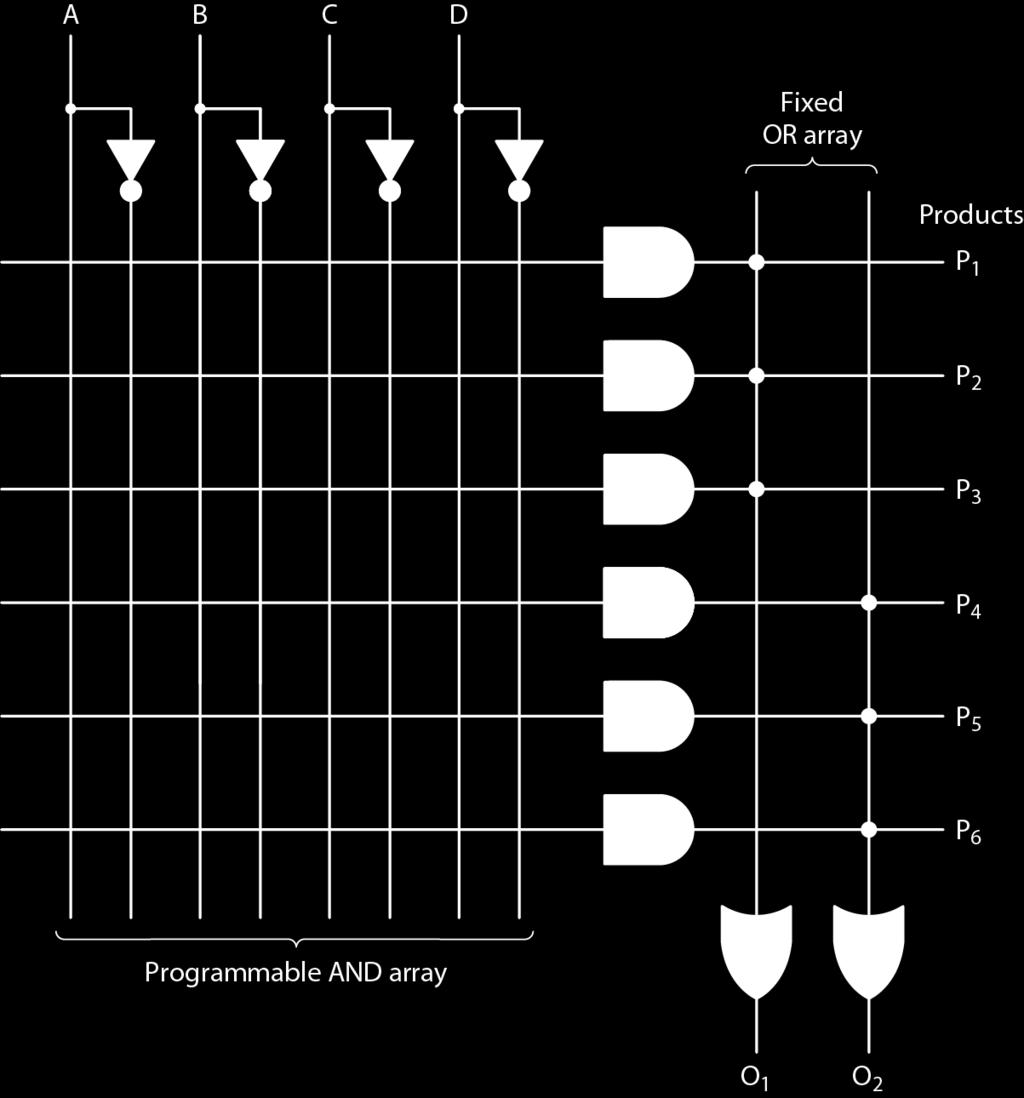
5 Basic Programmable Logic Array Organization
6 Two-Level AND-OR Arrays Realization of f(a,b,c) = abc + b c a a x b b x x c c x x x x abc + bc abc (b) bc Figure 5.5
7 a Multiple Functions Realized by an AND-OR Array x b c x x x x x x ab x c x bc f 1 (a, b, c) = ab + c f 2 (a, b, c) = ab + bc Figure 5.6
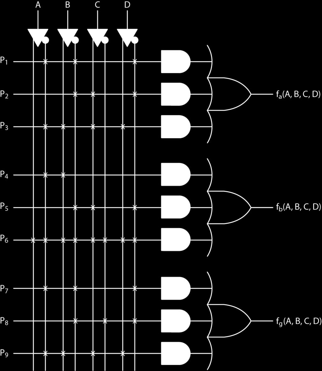
8 PLA Design -- Example 5.1 Design a PLA to realize the following 3 logic functions and show the internal connections. f 1 (A,B,C,D,E) = A B D + B CD + A BCDE f 2 (A,B,C,D,E) = A BE + B CD E f 3 (A,B,C,D,E) = A B D + B C D E + A BCD Since there are 5 inputs, there must be at least 5 inputs to the PLA, each of which must be both complemented and uncomplemented. There are a total of 7 unique product terms in the preceding 3 expressions. So the PLA must generate at least 7 product terms. Since 3 functions are being realized, there must be 3 sum (OR) terms generated.
9 Example 5.1 (continued) The PLA organization is shown in Fig Table 5.1 shows the connections that must be made in the AND and OR arrays. In the table, the product term numbers correspond to the AND gate numbers in Fig. 5.7, each connected to one vertical product line, on which a product term is generated. In the AND array portion of the table - a 0 indicates that the complement of the variable is connected to the product line - a 1 indicates the the uncomplemented input is connected to the product line - an indicates that neither is connected to the product line For the OR array, a 1 indicates a connection and a 0 indicates no connection.


10 PLA for Example 5.1 Figure 5.7
11 Table PLA Table for Example 5.1 AND Array Inputs OR Array Outputs Product Term ABCDE f 1 f 2 f A B D B CD A BCDE A BE B CD E B C D E A BCD
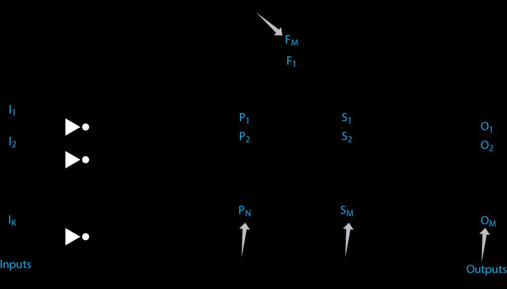
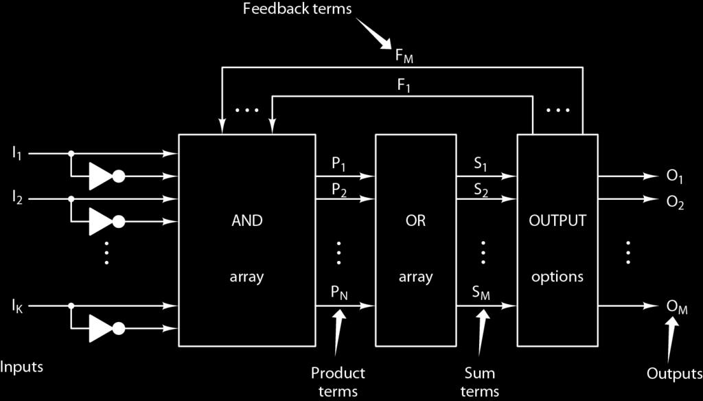
12 Basic Programmable Logic Array Organization
13 Output Polarity Options Inputs I l I k.... Active high (H) Active low (L) Active high Active low Complementary outputs (C) Programmable polarity (P) P l Product terms P m (a) +V Fuse Figure 5.11
14 Output Polarity Options(continued) S i x O i = S i S i O i = S i (b) (c) Figure 5.11
15 Implementation of SOP and POS Forms A * * B * * * C * * * * * * f 1 * * f 2 AB AC AB AC Figure 5.12
16 Bidirectional Pins and Feedback Lines A bidirectional pin is driven by a three-state driver, whose control line is connected to one of the product terms. When the control line is 1, the driver is said to be enabled and functions as a short circuit, as shown in Fig. 5.13b. In this case the sum term is driven onto the pin, which therefore functions as an output. This value is fed back to the AND array, where it can be used to form product terms. When the driver control line is 0, the driver is disabled and functions as an open circuit, as shown in Fig. 5.13c. This disconnects the sum term from the pin, which, through the feedback line, now becomes an input to the AND array.
17 Bidirectional Pins P 1... P n P n + 1 I 1 I k.. Feedback... IO m S m Three-state driver (a) Figure 5.13
18 Bidirectional Pins(continued) Feedback = S m Feedback = IO m S m (b) IO m (output) S m (c) IO m (input) Figure 5.13
19 Two-bit ripple-carry adder Example 5.3 Implement a 2-bit ripple-carry adder, as shown in Fig. 5.14a, using a programmable logic array having 4 dedicated input pins, 3 dedicated output pins, and 3 bidirectional pins. The standard logic equations for one state, i, of an n-bit full-adder are the following: S i = A i B i C i-1 + A i B i C i-1 + A i B i C i-1 + A i B i C i-1 C i = A i B i + A i C i-1 + B i C i-1 where A i and B i are the data inputs and C i-1 the carry input to stage i, S i is its sum output and C i the carry output. For a ripple-carry adder, the carry-out of one stage is connected to the carry input of the next stage, as shown in Fig. 5.14a.
20 Example 5.3(continued) Figure 5.14b shows the PLA implementation of the block diagram in Fig. 5.14a. Since the adder requires 5 inputs, and there are only 4 dedicated input pins, bidirectional pin 5 is used as another input. The driver of pin 5 is disabled by product line 16 by leaving all its fuses intact. Carry term C 0 is used to compute terms S 1 and C 1 through the feedback line from pin 6, allowing C 0 to be combined with A 1 and B 1 by the preceding equations.


21 Figure 5.14 Two-bit Ripple-carry Adder Example 5.3
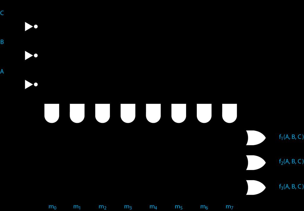
22 Programmable Read-only Memory A PROM comprises a fixed AND array and a programmable OR array, as illustrated in Fig The AND array generates all 2 n possible minterm products of its n inputs and therefore often referred to as an n-to-2 n decoder. The OR array allows any combination of product terms to be included in each sum term. The canonical sum of products form of any function can be realized directly from its truth table or minterm list. Figure 5.22 illustrates the organization of most typical commercial PROMs.
23 Programmable Read-only Memory (PROM) I 0 I 1 I 2 Fixed AND array Programmable OR array... O 1 O 2 O k m 0 m 1 m 2 m 3 m 4 m 5 m 6 m 7 Minterms Figure 5.21
24 General Configuration of a Commercial PROM Inputs A 0 A 1 A N-1.. AND array CE Chip enable. P 0 P 1 P2 N-1 OR array..... Product terms Output drivers O 1 O 2 O M Outputs Figure 5.22
25 Realizing Logic Functions with PROMs Each output of a PROM is capable of realizing any arbitrary switching function by connecting that output to the minterms of the function. To realize a given switching function with a PROM, first express the function in canonical SOP form or else derive the truth table of the function. Then, each of the minterms of the function is connected to the desired OR term to produce the canonical SOP form. It should be noted that the use of a commercially available PROM would be very inefficient when only a small number of minterms is needed, unless minimizing chip count is the primary goal.
26 PROM Realization -- Example 5.6 Realize the following 3 switching functions with a 3-input, 3-output PROM. f 1 (A, B, C) = AB + B C f 2 (A, B, C) = (A + B + C)(A + B) f 3 (A, B, C) = A + BC First, convert each function to canonical SOP form. f 1 (A, B, C) = ABC + ABC + A B C + AB C = m(1, 5, 6, 7) f 2 (A, B, C) = (A + B + C)(A + B + C )(A + B + C) = M(2, 4, 5) = m(0, 1, 3, 6, 7) f 3 (A, B, C) = AB C + ABC + AB C + ABC + A BC = m(3, 4, 5, 6, 7)

27 PROM Realization for Example 5.6 Figure 5.23
28 Lookup Tables (LUT) A common application of PROMs is the lookup table, in which a function is stored in tabular form with its arguments used as an index into the table to retrieve the value of the function for those arguments. Since truth tables can be readily realized by PROMs, lookup tables are implemented by writing them in truth table format and then realizing the truth table with a PROM.
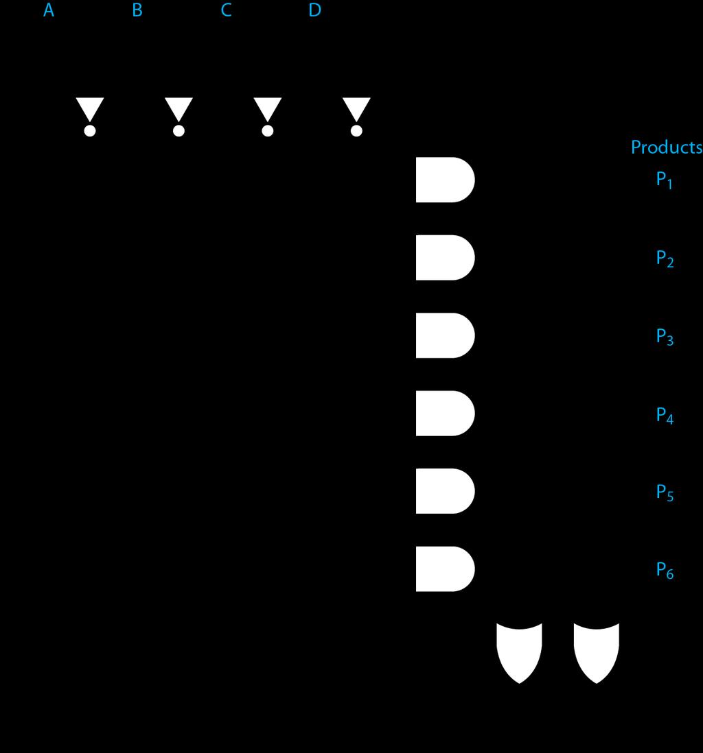
29 Programmable Array Logic (PAL)
30 Example 5.10 PAL Design Example Realize the following functions with a PAL f α (A,B,C,D) = A B D + B CD + A BCD f β (A,B,C,D) = A B + B CD f γ (A,B,C,D) = A B D + B C D + A BCD

31 Example PAL Realization
32 Complex Programmable Logic Devices (CPLDs)
33 Summary of Programmable Logic Devices PLA AND array and OR array are programmable PAL AND array programmable, OR array fixed PROM AND array fixed, OR programmable CPLD programmable array of PALs FPGA programmable array of logic elements

34 Cyclone II FPGA* LAB Logic Array Block, PLL Phase Locked Loop, IOEs I/O Elements *From Cyclone II Device Family Data Sheet
35 Cyclone II FPGA Family Features* *From Cyclone II Device Family Data Sheet
36 Cyclone II Package Options* *From Cyclone II Device Family Data Sheet
37 Cyclone II Device Resources* *From Cyclone II Device Family Data Sheet
38 Cyclone II Logic Element Architecture* *From Cyclone II Device Family Data Sheet
39 Cyclone II Logic Element in Normal Mode* *From Cyclone II Device Family Data Sheet
40 Cyclone II Logic Element in Arithmetic Mode* *From Cyclone II Device Family Data Sheet
Programmable Logic Devices
 Programmable Logic Devices Programmable Logic Devices Fig. (1) General structure of PLDs Programmable Logic Device (PLD): is an integrated circuit with internal logic gates and/or connections that can
Presentation 4: Programmable Combinational Devices
 Presentation 4: Programmable Combinational Devices Asst. Prof Dr. Ahmet ÖZKURT DEUEEE Based on the Presentation by Prof. Kim, Young Ho Dept. of Information Computer Engineering E-mail : yhkim@hyowon.cs.pusan.ac.kr
CHAPTER 9 MULTIPLEXERS, DECODERS, AND PROGRAMMABLE LOGIC DEVICES
 CHAPTER 9 MULTIPLEXERS, DECODERS, AND PROGRAMMABLE LOGIC DEVICES This chapter in the book includes: Objectives Study Guide 9.1 Introduction 9.2 Multiplexers 9.3 Three-State Buffers 9.4 Decoders and Encoders
B.Tech II Year I Semester (R13) Regular Examinations December 2014 DIGITAL LOGIC DESIGN
 Regular Examinations December 2014 DIGITAL LOGIC DESIGN") B.Tech II Year I Semester () Regular Examinations December 2014 (Common to IT and CSE) (a) If 1010 2 + 10 2 = X 10, then X is ----- Write the first 9 decimal digits in base 3. (c) What is meant by don
B.Tech II Year I Semester () Regular Examinations December 2014 (Common to IT and CSE) (a) If 1010 2 + 10 2 = X 10, then X is ----- Write the first 9 decimal digits in base 3. (c) What is meant by don
LSN 6 Programmable Logic Devices
 LSN 6 Programmable Logic Devices Department of Engineering Technology LSN 6 What Are PLDs? Functionless devices in base form Require programming to operate The logic function of the device is programmed
Programmable Logic Devices (PLDs)
") Programmable Logic Devices (PLDs) 212: Digital Design I, week 13 PLDs basically store binary information in a volatile/nonvolatile device. Data is specified by designer and physically inserted (Programmed)
Programmable Logic Devices (PLDs) 212: Digital Design I, week 13 PLDs basically store binary information in a volatile/nonvolatile device. Data is specified by designer and physically inserted (Programmed)
Topics. Midterm Finish Chapter 7
 Lecture 9 Topics Midterm Finish Chapter 7 ROM (review) Memory device in which permanent binary information is stored. Example: 32 x 8 ROM Five input lines (2 5 = 32) 32 outputs, each representing a memory
Unit 6 1.Random Access Memory (RAM) Chapter 3 Combinational Logic Design 2.Programmable Logic
 Chapter 3 Combinational Logic Design 2.Programmable Logic") EE 200: Digital Logic Circuit Design Dr Radwan E Abdel-Aal, COE Unit 6.Random Access Memory (RAM) Chapter 3 Combinational Logic Design 2. Logic Logic and Computer Design Fundamentals Part Implementation
EE 200: Digital Logic Circuit Design Dr Radwan E Abdel-Aal, COE Unit 6.Random Access Memory (RAM) Chapter 3 Combinational Logic Design 2. Logic Logic and Computer Design Fundamentals Part Implementation
Experiment 3: Logic Simplification
 Module: Logic Design Name:... University no:.. Group no:. Lab Partner Name: Mr. Mohamed El-Saied Experiment : Logic Simplification Objective: How to implement and verify the operation of the logical functions
DIGITAL CIRCUIT LOGIC UNIT 9: MULTIPLEXERS, DECODERS, AND PROGRAMMABLE LOGIC DEVICES
 DIGITAL CIRCUIT LOGIC UNIT 9: MULTIPLEXERS, DECODERS, AND PROGRAMMABLE LOGIC DEVICES 1 Learning Objectives 1. Explain the function of a multiplexer. Implement a multiplexer using gates. 2. Explain the
Programmable Logic Devices UNIT II DIGITAL SYSTEM DESIGN
 Programmable Logic Devices UNIT II DIGITAL SYSTEM DESIGN 2 3 4 5 6 7 8 9 2 3 4 5 6 7 8 9 2 Implementation in Sequential Logic 2 PAL Logic Implementation Design Example: BCD to Gray Code Converter A B
Programmable Logic Devices. Programmable Read Only Memory (PROM) Example
 Example") Programmable Logic Devices Programmable Logic Devices (PLDs) are the integrated circuits. They contain an array of AND gates & another array of OR gates. There are three kinds of PLDs based on the type
Programmable Logic Devices Programmable Logic Devices (PLDs) are the integrated circuits. They contain an array of AND gates & another array of OR gates. There are three kinds of PLDs based on the type
Code No: R Set No. 1
 Code No: R059210504 Set No. 1 II B.Tech I Semester Regular Examinations, November 2006 DIGITAL LOGIC DESIGN ( Common to Computer Science & Engineering, Information Technology and Computer Science & Systems
2.6 BOOLEAN FUNCTIONS
 2.6 BOOLEAN FUNCTIONS Binary variables have two values, either 0 or 1. A Boolean function is an expression formed with binary variables, the two binary operators AND and OR, one unary operator NOT, parentheses
PROGRAMMABLE LOGIC DEVICES
 PROGRAMMABLE LOGIC DEVICES Programmable logic devices (PLDs) are used for designing logic circuits. PLDs can be configured by the user to perform specific functions. The different types of PLDs available
Memory and Programmable Logic
 Memory and Programmable Logic Memory units allow us to store and/or retrieve information Essentially look-up tables Good for storing data, not for function implementation Programmable logic device (PLD),
Code No: R Set No. 1
 Code No: R059210504 Set No. 1 II B.Tech I Semester Regular Examinations, November 2007 DIGITAL LOGIC DESIGN ( Common to Computer Science & Engineering, Information Technology and Computer Science & Systems
Code No: 07A3EC03 Set No. 1
 Code No: 07A3EC03 Set No. 1 II B.Tech I Semester Regular Examinations, November 2008 SWITCHING THEORY AND LOGIC DESIGN ( Common to Electrical & Electronic Engineering, Electronics & Instrumentation Engineering,
Injntu.com Injntu.com Injntu.com R16
 1. a) What are the three methods of obtaining the 2 s complement of a given binary (3M) number? b) What do you mean by K-map? Name it advantages and disadvantages. (3M) c) Distinguish between a half-adder
CHAPTER-2 STRUCTURE OF BOOLEAN FUNCTION USING GATES, K-Map and Quine-McCluskey
 CHAPTER-2 STRUCTURE OF BOOLEAN FUNCTION USING GATES, K-Map and Quine-McCluskey 2. Introduction Logic gates are connected together to produce a specified output for certain specified combinations of input
R10. II B. Tech I Semester, Supplementary Examinations, May
 SET - 1 1. a) Convert the following decimal numbers into an equivalent binary numbers. i) 53.625 ii) 4097.188 iii) 167 iv) 0.4475 b) Add the following numbers using 2 s complement method. i) -48 and +31
HANSABA COLLEGE OF ENGINEERING & TECHNOLOGY (098) SUBJECT: DIGITAL ELECTRONICS ( ) Assignment
 SUBJECT: DIGITAL ELECTRONICS ( ) Assignment") Assignment 1. What is multiplexer? With logic circuit and function table explain the working of 4 to 1 line multiplexer. 2. Implement following Boolean function using 8: 1 multiplexer. F(A,B,C,D) = (2,3,5,7,8,9,12,13,14,15)
Assignment 1. What is multiplexer? With logic circuit and function table explain the working of 4 to 1 line multiplexer. 2. Implement following Boolean function using 8: 1 multiplexer. F(A,B,C,D) = (2,3,5,7,8,9,12,13,14,15)
SIR C.R.REDDY COLLEGE OF ENGINEERING, ELURU DEPARTMENT OF INFORMATION TECHNOLOGY LESSON PLAN
 SIR C.R.REDDY COLLEGE OF ENGINEERING, ELURU DEPARTMENT OF INFORMATION TECHNOLOGY LESSON PLAN SUBJECT: CSE 2.1.6 DIGITAL LOGIC DESIGN CLASS: 2/4 B.Tech., I SEMESTER, A.Y.2017-18 INSTRUCTOR: Sri A.M.K.KANNA
Fig. 6-1 Conventional and Array Logic Symbols for OR Gate
 6- (a) Conventional symbol (b) Array logic symbol Fig. 6- Conventional and Array Logic Symbols for OR Gate 2 Prentice Hall, Inc. 6-2 k address lines Read n data input lines emory unit 2 k words n bits
ECE 331 Digital System Design
 ECE 331 Digital System Design Tristate Buffers, Read-Only Memories and Programmable Logic Devices (Lecture #17) The slides included herein were taken from the materials accompanying Fundamentals of Logic
CS470: Computer Architecture. AMD Quad Core
 CS470: Computer Architecture Yashwant K. Malaiya, Professor malaiya@cs.colostate.edu AMD Quad Core 1 Architecture Layers Building blocks Gates, flip-flops Functional bocks: Combinational, Sequential Instruction
R07. Code No: V0423. II B. Tech II Semester, Supplementary Examinations, April
 SET - 1 II B. Tech II Semester, Supplementary Examinations, April - 2012 SWITCHING THEORY AND LOGIC DESIGN (Electronics and Communications Engineering) Time: 3 hours Max Marks: 80 Answer any FIVE Questions
Combinational Logic Circuits
 Chapter 3 Combinational Logic Circuits 12 Hours 24 Marks 3.1 Standard representation for logical functions Boolean expressions / logic expressions / logical functions are expressed in terms of logical
DIGITAL SYSTEM FUNDAMENTALS (ECE421) DIGITAL ELECTRONICS FUNDAMENTAL (ECE4220. PROGRAMMABLE LOGIC DEVICES (PLDs)
 DIGITAL ELECTRONICS FUNDAMENTAL (ECE4220. PROGRAMMABLE LOGIC DEVICES (PLDs)") COURSE / CODE DIGITAL SYSTEM FUNDAMENTALS (ECE421) DIGITAL ELECTRONICS FUNDAMENTAL (ECE4220 PROGRAMMABLE LOGIC DEVICES (PLDs) A PLD, or programmable logic device, is an electronic component that is used
COURSE / CODE DIGITAL SYSTEM FUNDAMENTALS (ECE421) DIGITAL ELECTRONICS FUNDAMENTAL (ECE4220 PROGRAMMABLE LOGIC DEVICES (PLDs) A PLD, or programmable logic device, is an electronic component that is used
COLLEGE OF ENGINEERING DEPARTMENT OF ELECTRICAL AND ELECTRONICS ENGINEERING QUESTION BANK SUBJECT CODE & NAME: EC 1312 DIGITAL LOGIC CIRCUITS UNIT I
 KINGS COLLEGE OF ENGINEERING DEPARTMENT OF ELECTRICAL AND ELECTRONICS ENGINEERING QUESTION BANK SUBJECT CODE & NAME: EC 1312 DIGITAL LOGIC CIRCUITS YEAR / SEM: III / V UNIT I NUMBER SYSTEM & BOOLEAN ALGEBRA
Code No: R Set No. 1
 Code No: R059210504 Set No. 1 II B.Tech I Semester Supplementary Examinations, February 2007 DIGITAL LOGIC DESIGN ( Common to Computer Science & Engineering, Information Technology and Computer Science
Embedded Controller Design. CompE 270 Digital Systems - 5. Objective. Application Specific Chips. User Programmable Logic. Copyright 1998 Ken Arnold 1
 CompE 270 Digital Systems - 5 Programmable Logic Ken Arnold Objective Application Specific ICs Introduce User Programmable Logic Common Architectures Programmable Array Logic Address Decoding Example Development
END-TERM EXAMINATION
 (Please Write your Exam Roll No. immediately) END-TERM EXAMINATION DECEMBER 2006 Exam. Roll No... Exam Series code: 100919DEC06200963 Paper Code: MCA-103 Subject: Digital Electronics Time: 3 Hours Maximum
Boolean Algebra. BME208 Logic Circuits Yalçın İŞLER
 Boolean Algebra BME28 Logic Circuits Yalçın İŞLER islerya@yahoo.com http://me.islerya.com 5 Boolean Algebra /2 A set of elements B There exist at least two elements x, y B s. t. x y Binary operators: +
CONTENTS CHAPTER 1: NUMBER SYSTEM. Foreword...(vii) Preface... (ix) Acknowledgement... (xi) About the Author...(xxiii)
 Preface... (ix) Acknowledgement... (xi) About the Author...(xxiii)") CONTENTS Foreword...(vii) Preface... (ix) Acknowledgement... (xi) About the Author...(xxiii) CHAPTER 1: NUMBER SYSTEM 1.1 Digital Electronics... 1 1.1.1 Introduction... 1 1.1.2 Advantages of Digital Systems...
CONTENTS Foreword...(vii) Preface... (ix) Acknowledgement... (xi) About the Author...(xxiii) CHAPTER 1: NUMBER SYSTEM 1.1 Digital Electronics... 1 1.1.1 Introduction... 1 1.1.2 Advantages of Digital Systems...
EECS 150 Homework 7 Solutions Fall (a) 4.3 The functions for the 7 segment display decoder given in Section 4.3 are:
 4.3 The functions for the 7 segment display decoder given in Section 4.3 are:") Problem 1: CLD2 Problems. (a) 4.3 The functions for the 7 segment display decoder given in Section 4.3 are: C 0 = A + BD + C + BD C 1 = A + CD + CD + B C 2 = A + B + C + D C 3 = BD + CD + BCD + BC C 4
Problem 1: CLD2 Problems. (a) 4.3 The functions for the 7 segment display decoder given in Section 4.3 are: C 0 = A + BD + C + BD C 1 = A + CD + CD + B C 2 = A + B + C + D C 3 = BD + CD + BCD + BC C 4
Chapter 13 Programmable Logic Device Architectures
 Chapter 13 Programmable Logic Device Architectures Chapter 13 Objectives Selected areas covered in this chapter: Describing different categories of digital system devices. Describing different types of
CMPE223/CMSE222 Digital Logic
 CMPE223/CMSE222 Digital Logic Optimized Implementation of Logic Functions: Strategy for Minimization, Minimum Product-of-Sums Forms, Incompletely Specified Functions Terminology For a given term, each
Specifying logic functions
 CSE4: Components and Design Techniques for Digital Systems Specifying logic functions Instructor: Mohsen Imani Slides from: Prof.Tajana Simunic and Dr.Pietro Mercati We have seen various concepts: Last
DKT 122/3 DIGITAL SYSTEM 1
 Company LOGO DKT 122/3 DIGITAL SYSTEM 1 BOOLEAN ALGEBRA (PART 2) Boolean Algebra Contents Boolean Operations & Expression Laws & Rules of Boolean algebra DeMorgan s Theorems Boolean analysis of logic circuits
Date Performed: Marks Obtained: /10. Group Members (ID):. Experiment # 04. Boolean Expression Simplification and Implementation
:. Experiment # 04. Boolean Expression Simplification and Implementation") Name: Instructor: Engr. Date Performed: Marks Obtained: /10 Group Members (ID):. Checked By: Date: Experiment # 04 Boolean Expression Simplification and Implementation OBJECTIVES: To understand the utilization
Name: Instructor: Engr. Date Performed: Marks Obtained: /10 Group Members (ID):. Checked By: Date: Experiment # 04 Boolean Expression Simplification and Implementation OBJECTIVES: To understand the utilization
Lecture 13: Memory and Programmable Logic
 Lecture 13: Memory and Programmable Logic Syed M. Mahmud, Ph.D ECE Department Wayne State University Aby K George, ECE Department, Wayne State University Contents Introduction Random Access Memory Memory
QUESTION BANK FOR TEST
 CSCI 2121 Computer Organization and Assembly Language PRACTICE QUESTION BANK FOR TEST 1 Note: This represents a sample set. Please study all the topics from the lecture notes. Question 1. Multiple Choice
II/IV B.Tech (Regular/Supplementary) DEGREE EXAMINATION. Answer ONE question from each unit.
 DEGREE EXAMINATION. Answer ONE question from each unit.") Hall Ticket Number: 14CS IT303 November, 2017 Third Semester Time: Three Hours Answer Question No.1 compulsorily. II/IV B.Tech (Regular/Supplementary) DEGREE EXAMINATION Common for CSE & IT Digital Logic
Hall Ticket Number: 14CS IT303 November, 2017 Third Semester Time: Three Hours Answer Question No.1 compulsorily. II/IV B.Tech (Regular/Supplementary) DEGREE EXAMINATION Common for CSE & IT Digital Logic
Module -7. Karnaugh Maps
 1 Module -7 Karnaugh Maps 1. Introduction 2. Canonical and Standard forms 2.1 Minterms 2.2 Maxterms 2.3 Canonical Sum of Product or Sum-of-Minterms (SOM) 2.4 Canonical product of sum or Product-of-Maxterms(POM)
Boolean Algebra and Logic Gates
 Boolean Algebra and Logic Gates Binary logic is used in all of today's digital computers and devices Cost of the circuits is an important factor Finding simpler and cheaper but equivalent circuits can
VALLIAMMAI ENGINEERING COLLEGE. SRM Nagar, Kattankulathur DEPARTMENT OF ELECTRONICS AND COMMUNICATION ENGINEERING EC6302 DIGITAL ELECTRONICS
 VALLIAMMAI ENGINEERING COLLEGE SRM Nagar, Kattankulathur-603 203 DEPARTMENT OF ELECTRONICS AND COMMUNICATION ENGINEERING EC6302 DIGITAL ELECTRONICS YEAR / SEMESTER: II / III ACADEMIC YEAR: 2015-2016 (ODD
CSCI 220: Computer Architecture I Instructor: Pranava K. Jha. Simplification of Boolean Functions using a Karnaugh Map
 CSCI 22: Computer Architecture I Instructor: Pranava K. Jha Simplification of Boolean Functions using a Karnaugh Map Q.. Plot the following Boolean function on a Karnaugh map: f(a, b, c, d) = m(, 2, 4,
ECE380 Digital Logic
 ECE38 Digital Logic Optimized Implementation of Logic Functions: Strategy for Minimization, Minimum Product-of-Sums Forms, Incompletely Specified Functions Dr. D. J. Jackson Lecture 8- Terminology For
R07
 www..com www..com SET - 1 II B. Tech I Semester Supplementary Examinations May 2013 SWITCHING THEORY AND LOGIC DESIGN (Com. to EEE, EIE, BME, ECC) Time: 3 hours Max. Marks: 80 Answer any FIVE Questions
Lecture (05) Boolean Algebra and Logic Gates
 Boolean Algebra and Logic Gates") Lecture (05) Boolean Algebra and Logic Gates By: Dr. Ahmed ElShafee ١ Minterms and Maxterms consider two binary variables x and y combined with an AND operation. Since eachv ariable may appear in either
Lecture (05) Boolean Algebra and Logic Gates By: Dr. Ahmed ElShafee ١ Minterms and Maxterms consider two binary variables x and y combined with an AND operation. Since eachv ariable may appear in either
Evolution of Implementation Technologies. ECE 4211/5211 Rapid Prototyping with FPGAs. Gate Array Technology (IBM s) Programmable Logic
 Programmable Logic") ECE 42/52 Rapid Prototyping with FPGAs Dr. Charlie Wang Department of Electrical and Computer Engineering University of Colorado at Colorado Springs Evolution of Implementation Technologies Discrete devices:
ECE 42/52 Rapid Prototyping with FPGAs Dr. Charlie Wang Department of Electrical and Computer Engineering University of Colorado at Colorado Springs Evolution of Implementation Technologies Discrete devices:
problem maximum score 1 10pts 2 8pts 3 10pts 4 12pts 5 7pts 6 7pts 7 7pts 8 17pts 9 22pts total 100pts
 University of California at Berkeley College of Engineering epartment of Electrical Engineering and Computer Sciences EECS150 J. Wawrzynek Spring 2003 2/21/03 Exam I Solutions Name: I number: This is a
PALs, GALs & CUPL. What is Programmable Logic?
 PALs, GALs & CUPL A lesson on Programmable Logic Devices and programming them using CUPL What is Programmable Logic? Digital integrated circuits where the Boolean function can be determined by the user.
Lecture 4: Implementation AND, OR, NOT Gates and Complement
 EE210: Switching Systems Lecture 4: Implementation AND, OR, NOT Gates and Complement Prof. YingLi Tian Feb. 13, 2018 Department of Electrical Engineering The City College of New York The City University
 www.vidyarthiplus.com Question Paper Code : 31298 B.E./B.Tech. DEGREE EXAMINATION, NOVEMBER/DECEMBER 2013. Third Semester Computer Science and Engineering CS 2202/CS 34/EC 1206 A/10144 CS 303/080230012--DIGITAL
Chapter 6 Selected Design Topics
 Logic and Computer Design Fundamentals Chapter 6 Selected Design Topics Part 4 Programmable Implementation Technologies Charles Kime & Thomas Kaminski 2008 Pearson Education, Inc. (Hyperlinks are active
Points Addressed in this Lecture. Standard form of Boolean Expressions. Lecture 4: Logic Simplication & Karnaugh Map
 Points Addressed in this Lecture Lecture 4: Logic Simplication & Karnaugh Map Professor Peter Cheung Department of EEE, Imperial College London Standard form of Boolean Expressions Sum-of-Products (SOP),
IT 201 Digital System Design Module II Notes
 IT 201 Digital System Design Module II Notes BOOLEAN OPERATIONS AND EXPRESSIONS Variable, complement, and literal are terms used in Boolean algebra. A variable is a symbol used to represent a logical quantity.
UNIT - V MEMORY P.VIDYA SAGAR ( ASSOCIATE PROFESSOR) Department of Electronics and Communication Engineering, VBIT
 Department of Electronics and Communication Engineering, VBIT") UNIT - V MEMORY P.VIDYA SAGAR ( ASSOCIATE PROFESSOR) contents Memory: Introduction, Random-Access memory, Memory decoding, ROM, Programmable Logic Array, Programmable Array Logic, Sequential programmable
UNIT - V MEMORY P.VIDYA SAGAR ( ASSOCIATE PROFESSOR) contents Memory: Introduction, Random-Access memory, Memory decoding, ROM, Programmable Logic Array, Programmable Array Logic, Sequential programmable
ECE/Comp Sci 352 Digital Systems Fundamentals Kewal K. Saluja and Yu Hen Hu Spring Logic and Computer Design Fundamentals.
 University of Wisconsin - Madison ECE/Comp Sci 352 Digital Systems Fundamentals Kewal K. Saluja and Yu Hen Hu Spring 2002 Chapter 6 Part 2 Memories & Programmable Logic Devices Originals by: Charles R.
R.M.D. ENGINEERING COLLEGE R.S.M. Nagar, Kavaraipettai
 L T P C R.M.D. ENGINEERING COLLEGE R.S.M. Nagar, Kavaraipettai- 601206 DEPARTMENT OF ELECTRONICS AND COMMUNICATION ENGINEERING EC8392 UNIT - I 3 0 0 3 OBJECTIVES: To present the Digital fundamentals, Boolean
CS8803: Advanced Digital Design for Embedded Hardware
 CS883: Advanced Digital Design for Embedded Hardware Lecture 2: Boolean Algebra, Gate Network, and Combinational Blocks Instructor: Sung Kyu Lim (limsk@ece.gatech.edu) Website: http://users.ece.gatech.edu/limsk/course/cs883
Combinational Logic Use the Boolean Algebra and the minimization techniques to design useful circuits No feedback, no memory Just n inputs, m outputs
 Combinational Logic Use the Boolean Algebra and the minimization techniques to design useful circuits No feedback, no memory Just n inputs, m outputs and an arbitrary truth table Analysis Procedure We
FPGA for Complex System Implementation. National Chiao Tung University Chun-Jen Tsai 04/14/2011
 FPGA for Complex System Implementation National Chiao Tung University Chun-Jen Tsai 04/14/2011 About FPGA FPGA was invented by Ross Freeman in 1989 SRAM-based FPGA properties Standard parts Allowing multi-level
DHANALAKSHMI SRINIVASAN COLLEGE OF ENGINEERING AND TECHNOLOGY
 DHANALAKSHMI SRINIVASAN COLLEGE OF ENGINEERING AND TECHNOLOGY Dept/Sem: II CSE/03 DEPARTMENT OF ECE CS8351 DIGITAL PRINCIPLES AND SYSTEM DESIGN UNIT I BOOLEAN ALGEBRA AND LOGIC GATES PART A 1. How many
Recitation Session 6
 Recitation Session 6 CSE341 Computer Organization University at Buffalo radhakri@buffalo.edu March 11, 2016 CSE341 Computer Organization Recitation Session 6 1/26 Recitation Session Outline 1 Overview
Programmable Logic Devices I. EECE143 Lecture 4. PALs, GALs & CUPL. A lesson on Programmable Logic Devices and programming them using CUPL
 PALs, GALs & CUPL A lesson on Programmable Logic Devices and programming them using CUPL What is Programmable Logic? Digital integrated circuits where the Boolean function can be determined by the user.
Memory and Programmable Logic
 Digital Circuit Design and Language Memory and Programmable Logic Chang, Ik Joon Kyunghee University Memory Classification based on functionality ROM : Read-Only Memory RWM : Read-Write Memory RWM NVRWM
Workshop on Digital Circuit Design in FPGA
 Workshop on Digital Circuit Design in FPGA Session-1 Presented By Mohammed Abdul Kader Assistant Professor, Dept. of EEE, IIUC Email:kader05cuet@gmail.com Website: kader05cuet.wordpress.com The field-programmable
(ii) Simplify and implement the following SOP function using NOR gates:
 Simplify and implement the following SOP function using NOR gates:") DHANALAKSHMI COLLEGE OF ENGINEERING DEPARTMENT OF ELECTRONICS AND COMMUNICATION ENGINEERING EE6301 DIGITAL LOGIC CIRCUITS UNIT I NUMBER SYSTEMS AND DIGITAL LOGIC FAMILIES PART A 1. How can an OR gate be
DHANALAKSHMI COLLEGE OF ENGINEERING DEPARTMENT OF ELECTRONICS AND COMMUNICATION ENGINEERING EE6301 DIGITAL LOGIC CIRCUITS UNIT I NUMBER SYSTEMS AND DIGITAL LOGIC FAMILIES PART A 1. How can an OR gate be
Digital Electronics 27. Digital System Design using PLDs
 1 Module -27 Digital System Design 1. Introduction 2. Digital System Design 2.1 Standard (Fixed function) ICs based approach 2.2 Programmable ICs based approach 3. Comparison of Digital System Design approaches
Review. EECS Components and Design Techniques for Digital Systems. Lec 03 Field Programmable Gate Arrays
 EECS 5 - Components and Design Techniques for Digital Systems Lec 3 Field Programmable Gate Arrays 9-4-7 David Culler Electrical Engineering and Computer Sciences University of California, Berkeley http://www.eecs.berkeley.edu/~culler
SIDDHARTH GROUP OF INSTITUTIONS :: PUTTUR Siddharth Nagar, Narayanavanam Road QUESTION BANK (DESCRIPTIVE)
") SIDDHARTH GROUP OF INSTITUTIONS :: PUTTUR Siddharth Nagar, Narayanavanam Road 517583 QUESTION BANK (DESCRIPTIVE) Subject with Code : STLD(16EC402) Year & Sem: II-B.Tech & I-Sem Course & Branch: B.Tech
SIDDHARTH GROUP OF INSTITUTIONS :: PUTTUR Siddharth Nagar, Narayanavanam Road 517583 QUESTION BANK (DESCRIPTIVE) Subject with Code : STLD(16EC402) Year & Sem: II-B.Tech & I-Sem Course & Branch: B.Tech
MEMORY AND PROGRAMMABLE LOGIC
 MEMORY AND PROGRAMMABLE LOGIC Memory is a device where we can store and retrieve information It can execute a read and a write Programmable Logic is a device where we can store and retrieve information
INSTITUTE OF AERONAUTICAL ENGINEERING (Autonomous) Dundigal, Hyderabad
 Dundigal, Hyderabad") INSTITUTE OF AERONAUTICAL ENGINEERING (Autonomous) Dundigal, Hyderabad - 500 043 COMPUTER SCIENCE AND ENGINEERING TUTORIAL QUESTION BANK Name : DIGITAL LOGIC DESISN Code : AEC020 Class : B Tech III Semester
INSTITUTE OF AERONAUTICAL ENGINEERING (Autonomous) Dundigal, Hyderabad - 500 043 COMPUTER SCIENCE AND ENGINEERING TUTORIAL QUESTION BANK Name : DIGITAL LOGIC DESISN Code : AEC020 Class : B Tech III Semester
I 4 I 3 I 2 I 1 I 0 A 7 A 6 A 5 A 4 A 3 A 2 A 1 A 0 T-125. ROM Truth Table (Partial) 1997 by Prentice-Hall, Inc.
 1997 by Prentice-Hall, Inc.") 997 by Prentice-Hall, Inc. ano & Kime Upper Saddle River, New Jersey 7458 T-5 Inputs Outputs I 4 I 3 I I I A 7 A 6 A 5 A 4 A 3 A A A...... RO Truth Table (Partial) 997 by Prentice-Hall, Inc. ano & Kime
997 by Prentice-Hall, Inc. ano & Kime Upper Saddle River, New Jersey 7458 T-5 Inputs Outputs I 4 I 3 I I I A 7 A 6 A 5 A 4 A 3 A A A...... RO Truth Table (Partial) 997 by Prentice-Hall, Inc. ano & Kime
10EC33: DIGITAL ELECTRONICS QUESTION BANK
 10EC33: DIGITAL ELECTRONICS Faculty: Dr.Bajarangbali E Examination QuestionS QUESTION BANK 1. Discuss canonical & standard forms of Boolean functions with an example. 2. Convert the following Boolean function
Hours / 100 Marks Seat No.
 17333 13141 3 Hours / 100 Seat No. Instructions (1) All Questions are Compulsory. (2) Answer each next main Question on a new page. (3) Illustrate your answers with neat sketches wherever necessary. (4)
Digital logic fundamentals. Question Bank. Unit I
 Digital logic fundamentals Question Bank Subject Name : Digital Logic Fundamentals Subject code: CA102T Staff Name: R.Roseline Unit I 1. What is Number system? 2. Define binary logic. 3. Show how negative
UNIT- V COMBINATIONAL LOGIC DESIGN
 UNIT- V COMBINATIONAL LOGIC DESIGN NOTE: This is UNIT-V in JNTUK and UNIT-III and HALF PART OF UNIT-IV in JNTUA SYLLABUS (JNTUK)UNIT-V: Combinational Logic Design: Adders & Subtractors, Ripple Adder, Look
VALLIAMMAI ENGINEERING COLLEGE
 VALLIAMMAI ENGINEERING COLLEGE SRM Nagar, Kattankulathur 603 203 DEPARTMENT OF INFORMATION TECHNOLOGY QUESTION BANK Academic Year 2018 19 III SEMESTER CS8351-DIGITAL PRINCIPLES AND SYSTEM DESIGN Regulation
INSTITUTE OF AERONAUTICAL ENGINEERING (Autonomous) Dundigal, Hyderabad
 Dundigal, Hyderabad") INSTITUTE OF AERONAUTICAL ENGINEERING (Autonomous) Dundigal, Hyderabad - 500043 Course Name : DIGITAL LOGIC DESISN Course Code : AEC020 Class : B Tech III Semester Branch : CSE Academic Year : 2018 2019
INSTITUTE OF AERONAUTICAL ENGINEERING (Autonomous) Dundigal, Hyderabad - 500043 Course Name : DIGITAL LOGIC DESISN Course Code : AEC020 Class : B Tech III Semester Branch : CSE Academic Year : 2018 2019
Experiment 4 Boolean Functions Implementation
 Experiment 4 Boolean Functions Implementation Introduction: Generally you will find that the basic logic functions AND, OR, NAND, NOR, and NOT are not sufficient to implement complex digital logic functions.
Chap-2 Boolean Algebra
 Chap-2 Boolean Algebra Contents: My name Outline: My position, contact Basic information theorem and postulate of Boolean Algebra. or project description Boolean Algebra. Canonical and Standard form. Digital
Lecture 7. Standard ICs FPGA (Field Programmable Gate Array) VHDL (Very-high-speed integrated circuits. Hardware Description Language)
 VHDL (Very-high-speed integrated circuits. Hardware Description Language)") Standard ICs FPGA (Field Programmable Gate Array) VHDL (Very-high-speed integrated circuits Hardware Description Language) 1 Standard ICs PLD: Programmable Logic Device CPLD: Complex PLD FPGA: Field Programmable
Standard ICs FPGA (Field Programmable Gate Array) VHDL (Very-high-speed integrated circuits Hardware Description Language) 1 Standard ICs PLD: Programmable Logic Device CPLD: Complex PLD FPGA: Field Programmable
Hours / 100 Marks Seat No.
 17320 21718 3 Hours / 100 Seat No. Instructions (1) All Questions are Compulsory. (2) Answer each next main Question on a new page. (3) Figures to the right indicate full marks. (4) Assume suitable data,
Programmable Logic Devices
 Programmable Logic Devices INTRODUCTION A programmable logic device or PLD is an electronic component used to build reconfigurable digital circuits. Unlike a logic gate, which has a fixed function, a PLD
VALLIAMMAI ENGINEERING COLLEGE
 VALLIAMMAI ENGINEERING COLLEGE SRM Nagar, Kattankulathur 603 203 DEPARTMENT OF INFORMATION TECHNOLOGY & COMPUTER SCIENCE AND ENGINEERING QUESTION BANK II SEMESTER CS6201- DIGITAL PRINCIPLE AND SYSTEM DESIGN
Chapter 2 Combinational
 Computer Engineering 1 (ECE290) Chapter 2 Combinational Logic Circuits Part 2 Circuit Optimization HOANG Trang 2008 Pearson Education, Inc. Overview Part 1 Gate Circuits and Boolean Equations Binary Logic
EEE130 Digital Electronics I Lecture #4_1
 EEE130 Digital Electronics I Lecture #4_1 - Boolean Algebra and Logic Simplification - By Dr. Shahrel A. Suandi 4-6 Standard Forms of Boolean Expressions There are two standard forms: Sum-of-products form
Question Total Possible Test Score Total 100
 Computer Engineering 2210 Final Name 11 problems, 100 points. Closed books, closed notes, no calculators. You would be wise to read all problems before beginning, note point values and difficulty of problems,
FYSE420 DIGITAL ELECTRONICS. Lecture 7
 FYSE420 DIGITAL ELECTRONICS Lecture 7 1 [1] [2] [3] DIGITAL LOGIC CIRCUIT ANALYSIS & DESIGN Nelson, Nagle, Irvin, Carrol ISBN 0-13-463894-8 DIGITAL DESIGN Morris Mano Fourth edition ISBN 0-13-198924-3
SHRI ANGALAMMAN COLLEGE OF ENGINEERING. (An ISO 9001:2008 Certified Institution) SIRUGANOOR, TIRUCHIRAPPALLI
 SIRUGANOOR, TIRUCHIRAPPALLI") SHRI ANGALAMMAN COLLEGE OF ENGINEERING AND TECHNOLOGY (An ISO 9001:2008 Certified Institution) SIRUGANOOR, TIRUCHIRAPPALLI 621 105 DEPARTMENT OF ELECTRONICS AND COMMUNICATION ENGINEERING EC1201 DIGITAL
SHRI ANGALAMMAN COLLEGE OF ENGINEERING AND TECHNOLOGY (An ISO 9001:2008 Certified Institution) SIRUGANOOR, TIRUCHIRAPPALLI 621 105 DEPARTMENT OF ELECTRONICS AND COMMUNICATION ENGINEERING EC1201 DIGITAL
R a) Simplify the logic functions from binary to seven segment display code converter (8M) b) Simplify the following using Tabular method
 Simplify the logic functions from binary to seven segment display code converter (8M) b) Simplify the following using Tabular method") SET - 1 1. a) Convert the decimal number 250.5 to base 3, base 4 b) Write and prove de-morgan laws c) Implement two input EX-OR gate from 2 to 1 multiplexer (3M) d) Write the demerits of PROM (3M) e) What
SET - 1 1. a) Convert the decimal number 250.5 to base 3, base 4 b) Write and prove de-morgan laws c) Implement two input EX-OR gate from 2 to 1 multiplexer (3M) d) Write the demerits of PROM (3M) e) What
ece5745-pla-notes.txt
 ece5745-pla-notes.txt ========================================================================== Follow up on PAL/PROM/PLA Activity ==========================================================================
Unit-IV Boolean Algebra
 Unit-IV Boolean Algebra Boolean Algebra Chapter: 08 Truth table: Truth table is a table, which represents all the possible values of logical variables/statements along with all the possible results of
Optimized Implementation of Logic Functions
 June 25, 22 9:7 vra235_ch4 Sheet number Page number 49 black chapter 4 Optimized Implementation of Logic Functions 4. Nc3xe4, Nb8 d7 49 June 25, 22 9:7 vra235_ch4 Sheet number 2 Page number 5 black 5 CHAPTER
1. Mark the correct statement(s)
") 1. Mark the correct statement(s) 1.1 A theorem in Boolean algebra: a) Can easily be proved by e.g. logic induction b) Is a logical statement that is assumed to be true, c) Can be contradicted by another
1. Mark the correct statement(s) 1.1 A theorem in Boolean algebra: a) Can easily be proved by e.g. logic induction b) Is a logical statement that is assumed to be true, c) Can be contradicted by another
Question No: 1 ( Marks: 1 ) - Please choose one A SOP expression is equal to 1
 - Please choose one A SOP expression is equal to 1") ASSALAM O ALAIKUM all fellows ALL IN ONE Mega File CS302 Midterm PAPERS, MCQz & subjective Created BY Farhan& Ali BS (cs) 3rd sem Hackers Group Mandi Bahauddin Remember us in your prayers Mindhacker124@gmail.com
ASSALAM O ALAIKUM all fellows ALL IN ONE Mega File CS302 Midterm PAPERS, MCQz & subjective Created BY Farhan& Ali BS (cs) 3rd sem Hackers Group Mandi Bahauddin Remember us in your prayers Mindhacker124@gmail.com