The Itanium Bit Microprocessor Report
|
|
|
- Hollie Lindsey
- 5 years ago
- Views:
Transcription
1 The Itanium Bit Microprocessor Report By PRIYANK JAIN ( ) Group # 11 Under guidance of Dr. J. K. Deka & Dr. S. B. Nair Department of Computer Science & Engineering Indian Institute of Technology, Guwahati. Date : April 21,
2 TABLE OF CONTENTS 2 Design Requirements... 4 Characteristics... 4 Functions Implemented... 4 Design Characteristics... 5 Design on a CISC based architecture... 5 Microprogramming logic used... 5 Control Unit Design... 5 Basic Architecture... 6 Clocking Mechanism... 6 Memory Interfacing... 7 Hardware Requirements... 8 Instruction Set... 9 LOAD... 9 STORE... 9 JUMP ADD(Data) AND CALL MOVE (A->B) NOT SUB(Reg) JUMP(A=B) RETURN MULTIPLY SUB(Data) ADD(Reg) MOVE(B->A) HALT Design and Implementation Register Organization Special Registers Memory Data Register Memory Address Register Program Counter Stack Register Micro Program Counter Micro Instruction Register Accumulator General Purpose Registers Subroutine Support Jump Support
3 Design Requirements : Characteristics 8 bit Data bus. 8 bit Address bus. 3 general purpose register Functions Implemented Memory Access instructions: 1. Load 2. Store Arithmetic Operations: 3. Add (data) 4. Add (registers) 5. Multiply 6. Subtract (data) 7. Subtract (registers) Logical Operations: 8. NOT 9. OR 10. AND Internal Register Access : 11. Move (A->B) 12. Move (B->A) Control Transfer Instructions: 13. Jump (unconditional) 14. Jump (conditional) 15. Call 16. Return 17. Halt 4
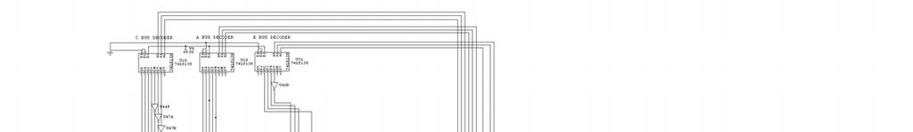
4 Design Characteristics : Design on a CISC based architecture Microprogramming logic used. Control Unit Design The CPU has a MICRO PROGRAMMED CONTROL UNIT. The design features characteristics state of CISC Architecture. 4 EPROM s(erasable Programmable Read only memory Chips) were used for this purpose. A total of 32 control signals were used. EPROM 1 Add7 ADDRESS LINES TO JUMP TO Add6 Add5 Add4 Add3 Add2 Add1 Add0 EPROM 2 A3 ADDRESS BITS FOR A DECODER A2 A1 B3 ADDRESS BITS FOR B DECODER B2 B1 MDR (READ) MDR (WRITE) 5
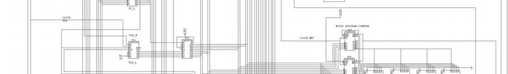
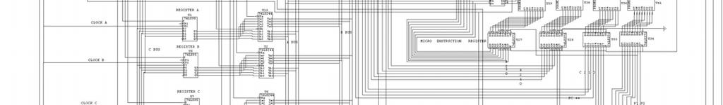
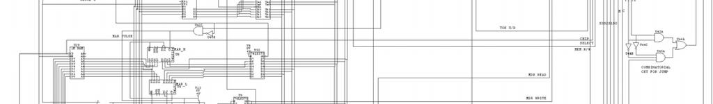
5 EPROM 3 C3 ADDRESS BITS FOR C DECODER C2 C1 PC++ SIGNAL TO INCREMENT PC TOS UP/DOWN SIGNAL FOR SP LE LATCH ENABLE FOR FLAG LATCH CS CHIP SELECT(FOR MAIN MEMORY) R/W READ/WRITE (FOR MAIN MEMORY) EPROM 4 S3 4 SELECT LINES FOR ALU S2 S1 S0 M 2 ARITHMETIC/LOGIC LINES FOR ALU C P1 2 CONDITION BITS P2 Basic Architecture The basic architecture of the CPU consists of a set of registers ( special purpose and general purpose ),some of which are connected to A and B buses which is in turn connected to the ALU. The arithmetic and logic operations are performed by the ALU. Connected to these buses are the MAR(memory address register) and MDR(memory data register) which are directly connected to the RAM chip 6116(having 8 data lines and 8 address lines).the clock subcycle generator (JHONSON counter ) sends clock pulses to all the above entities. The control signals and the select lines are provided by the MICRO INSTRUCTION register (which is connected to the MICRO CONTROL STORE). Clocking Mechanism A JHONSON counter has been used to generate 4 subcycles which supply the clock to the entire CPU. The principle of JHONSON counter is that just 1 bit of the 4 bit shift register 7495 is kept high. The highest bit is again fed into the serial input to generate 4 clock pulses with a phase shift. 6
6 As can be seen Q3 is fed into Ds. Shift clock is the main clock of the CPU. Discreet waveforms having a phase shift can thus be obtained. The following actions are performed at each clock sub-cycle CLOCK SUBCYCLE 1: The latch of the MICRO INSTRUCTION REGISTER is enabled during this clock cycle. CLOCK SUBCYCLE 2: A & B latches latch on to the values of the A and B bus respectively. CLOCK SUBCYCLE 3: MEMORY ADDRESS REGISTER takes in the address from the A and B buses. CLOCK SUBCYCLE 4: All the special purpose and general purpose registers get the 4 th clock sub-cycle. Memory Interfacing The Main Memory consists of the RAM chip The actual size of the memory is 2 X1024 X 8 bits. But in this architecture only 8 address lines are used ie. 256 memory locations are accessed. The data bus is used for both load as well as store operations. Tri-state buffers are used so that the same bus can be used for both read and write operations. The two very important registers used to interface the internal logistics of the CPU with the main memory are - 1) MEMORY ADDRESS REGISTER 2) MEMORY DATA REGISTER 7
7 Hardware Requirements Primitive IC s ( 74XXX, RAM, ROM) Power Supply TTL Logic Clock Input IC s Used 1. SRAM 6116 ( 8 bit data bus & 11 bit Address Bus ) X 1 2. EPROM INTEL 2732 X 4 3. ALU ( 4 bit,16 function ) X ( 4X16 Decoder ) X ( 4 bit Shift Register With PL) X ( 4 bit Universal Register ) X ( 4 bit Up / Dn. Counter) X ( 4 bit up counter ) X ( 8 bit latch) X (4 bit Latch) X (Hex Tri-state Buffer) X (Hex Inverter) X (Quad AND Gate) X (Quad OR Gate) X (BCD to 7 Segment Decoder) X (7 Segment Display) X 3 Power Supply +5 V and 0 V D.C Supply for all ICs. Clock Input A Frequency generator was used to provide a TTL logic clock. Circuit was tested to be functional for KHz frequency Range. 8
8 Instruction Set The CPU is designed to execute a set of 17 instructions an 8-bit opcode is required. This is the op-code assignment for each instruction. LOAD STORE JUMP ADD(DATA) AND CALL MOVE(A-B) NOT SUB(REG) JUMP(A=B) RETURN MULTIPLY SUB(DATA) ADD(REG) MOVE(B >A) HALT OR Table 3.1 Instruction Set To execute an instruction one needs to give an 8 - bit opcode followed by 4-bit operand. The CPU has four general purpose registers, thus 2 bits are required to reference one register. Thus using four bits 2 registers can be referenced. The context in which the register is referenced is instruction specific. LOAD This is one of the two memory access instructions. This is used to bring the contents of a memory location into the registers of the CPU. Its opcode is and the operand is used to specify the address which should be accessed. The content of the memory location is stored into the accumulator STORE This is the other instruction that accesses the memory. This is used to store the content of registers into the main memory. The construct is similar to that of LOAD. Its opcode and the operand is used to specify the address where the where the data has to be stored. When this instruction is executed the contents of the accumulator is stored into the memory. 9
9 JUMP This is the unconditional jump statement. It is used to set the program counter to a value of the succeeding location. It opcode is The operand is used to specify the 8 bit jump address. ADD (Data) This is an arithmetic instruction which uses the ALU. Its opcode is The operand is used to specify the value to be added to the accumulator. The result of the operation is stored in the accumulator. The carry bit is not handled in this architecture. AND This is a logical operation and uses the ALU. Its opcode is This performs bitwise AND operation on the content of the accumulator with the operand. The result of the operation is stored in the accumulator CALL This is the instruction used to make a subroutine call. When this is done the current value of program counter (PC) is stored in the stack register and then the program counter is set to the value depending on the location to which the call takes place. Its opcode is MOVE (A->B) This is used to copy the content of register A into B. Its opcode is This instruction is very significant as the results of all alu and memory operations are stored in the accumulator. NOT This is a logical instruction in which bit wise binary inversion is done. Its opcode is The result of this operation is stored in the accumulator (register A) SUB (Reg) This is an arithmetic instruction. Its opcode is The difference is stored in the accumulator. The architecture supports negative numbers. JUMP (A=B) This is a the conditional counterpart to the jump statement. In this statement the jump occurs only if the contents of the registers A & B are same. Its opcode is The operand is used to specify the address locations to jump to. 10
10 RETURN This is used to return from a subroutine call. When this instruction is executed the contents of the stack register is set into the program counter. Thus the program continues execution from the location following the one from which call took place. Its opcode is MULTIPLY This is an arithmetic instruction. Its opcode is The result is stored in the accumulator. The architecture does not support negative numbers. SUB (Data) This is an arithmetic instruction. Its opcode is The operand is used to specify the value which is to be subtracted from the accumulator. The difference is stored in the accumulator. The architecture does support negative numbers. ADD (Reg) This is an arithmetic instruction which uses the ALU. Its opcode is The result of the operation is stored in the accumulator. The carry bit is not handled in this architecture. MOVE (B->A) This is used to copy the content of one register into another. Its opcode is This instruction is very significant as the results of all alu and memory operations are stored in the accumulator. OR This is another logical operation. Its opcode is This performs bitwise OR operation on the contents of the registers specified by the operand and stores the result of the operation in the accumulator. HALT This is the instruction used to signify the end of the program. It opcode is After this instruction the clock to the entire CPU is disabled. The state of the registers are frozen and they continue to store the value last held by them. This instruction is irreversible and execution cannot be continued without putting the power back on again. 11
11 Design and Implementation Register Organization The registers in the architecture can be broadly divided into two categories, special registers and general purpose registers. This classification is by no means mutually exclusive and some registers seem to have characteristics of both especially the accumulator. Special Registers Memory Data Register This is the register which is connected to the data lines of the memory. Any value which is to be written onto the memory first gets stored in the memory data register. Also any data or address to be read from the main memory gets stored in the M.D.R Memory Address Register This is the register which is connected to address lines of the main memory. The address location to be referenced is transferred from the bus onto the M.A.R Program Counter This is the register which is used to store the address location of the next instruction. Its value is to changed during the JUMP instruction. Also during CALL and RETURN program counter s value is to be stored and retrieved from the stack. It actually consists of two 4 bit registers. Stack Register This is the register where the program counter is stored when a CALL instruction takes place. The stack register actually consists of two 4 bit registers. This register stores the program counter. The value stored in this register is used to reset the program counter in the case of RETURN. Micro Program Counter This is the register which is used to reference the Micro Control Store(EPROM s).the Instruction from the main memory is directly translated into the address location of the Micro Control Store, where the Micro Program has already been stored. 12
12 Micro Instruction Register All the 32 control signals get latched onto the Micro instruction Register at the 1 st clock pulse. Then the micro instruction register sends all the control signals to the respective decoders and select lines. Accumulator This can be considered to be a special general purpose register. This is a register that is available to the programmer space. This is the register where all the results of all ALU operations are stored. This is also the only register which can interact with the RAM memory by means of LOAD and STORE. Assignment operation can also take place only into this register. This register is referred to by A. Accumulator can perform all the functions that can be performed by all other registers and can be used for all manipulations by the programmer. General Purpose Registers They are three in number including the accumulator. The programmer can use them for both data storage and manipulation. When the CPU starts these register are set to an arbitary value. They can be used as input to the ALU; either as first operand or second, but the result of the ALU operation comes into the accumulator and has to be shifted to other register by means of MOVE instruction. Subroutine Support The architecture has built in support for function call. A programmer may make a subroutine call to any location in the program store, execute instructions there and then jump back to the initial location. He is not required to handle to which location he has to jump back to. This is handled by the architecture. More than one levels of subroutine calls is supported. Thus recursion is automatically supported. At the heart of the subroutine call support is the two stack registers. These register stores the value of the program counter whenever a function call takes place. This value is set back into the program counter whenever a return statement is encountered. Jump Support The architecture supports two kinds of jump statements. In both cases the appropriate value as specified in the operands is set in the program counter. There are two types of jumps. An unconditional jump where the jump always takes place and a conditional jump in which case the jump takes place only if the contents of the register A and B are same. For conditional jump a comparator is used. A flag register was maintained and thus ALU output could be used for a jump. 13
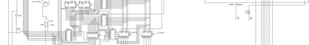
13 DETAILED CIRCUIT DIAGRAM 14
14 15
15 16
16 17
17 18
Microcomputer Architecture and Programming
 IUST-EE (Chapter 1) Microcomputer Architecture and Programming 1 Outline Basic Blocks of Microcomputer Typical Microcomputer Architecture The Single-Chip Microprocessor Microprocessor vs. Microcontroller
Introduction to Computers - Chapter 4
 Introduction to Computers - Chapter 4 Since the invention of the transistor and the first digital computer of the 1940s, computers have been increasing in complexity and performance; however, their overall
1 MALP ( ) Unit-1. (1) Draw and explain the internal architecture of 8085.
 Unit-1. (1) Draw and explain the internal architecture of 8085.") (1) Draw and explain the internal architecture of 8085. The architecture of 8085 Microprocessor is shown in figure given below. The internal architecture of 8085 includes following section ALU-Arithmetic
(1) Draw and explain the internal architecture of 8085. The architecture of 8085 Microprocessor is shown in figure given below. The internal architecture of 8085 includes following section ALU-Arithmetic
EXPERIMENT NO. 1 THE MKT 8085 MICROPROCESSOR TRAINER
 OBJECT: EXPERIMENT NO. 1 THE MKT 8085 MICROPROCESSOR TRAINER To understand the structure and operating instruction of the microprocessor trainer. INTRODUCTION: The MKT 8085 is a single-board microcomputer,
Computer Architecture
 Computer Architecture Lecture 1: Digital logic circuits The digital computer is a digital system that performs various computational tasks. Digital computers use the binary number system, which has two
Chapter 1: Basics of Microprocessor [08 M]
![Chapter 1: Basics of Microprocessor [08 M]](/thumbs/77/75860546.jpg "Chapter 1: Basics of Microprocessor [08 M]") Microprocessor: Chapter 1: Basics of Microprocessor [08 M] It is a semiconductor device consisting of electronic logic circuits manufactured by using either a Large scale (LSI) or Very Large Scale (VLSI)
Microprocessor: Chapter 1: Basics of Microprocessor [08 M] It is a semiconductor device consisting of electronic logic circuits manufactured by using either a Large scale (LSI) or Very Large Scale (VLSI)
Chapter 16. Control Unit Operation. Yonsei University
 Chapter 16 Control Unit Operation Contents Micro-Operation Control of the Processor Hardwired Implementation 16-2 Micro-Operations Micro-Operations Micro refers to the fact that each step is very simple
Lecture1: introduction. Outline: History overview Central processing unite Register set Special purpose address registers Datapath Control unit
 Lecture1: introduction Outline: History overview Central processing unite Register set Special purpose address registers Datapath Control unit 1 1. History overview Computer systems have conventionally
Digital System Design Using Verilog. - Processing Unit Design
 Digital System Design Using Verilog - Processing Unit Design 1.1 CPU BASICS A typical CPU has three major components: (1) Register set, (2) Arithmetic logic unit (ALU), and (3) Control unit (CU) The register
Basics of Microprocessor
 Unit 1 Basics of Microprocessor 1. Microprocessor Microprocessor is a multipurpose programmable integrated device that has computing and decision making capability. This semiconductor IC is manufactured
Class Notes. Dr.C.N.Zhang. Department of Computer Science. University of Regina. Regina, SK, Canada, S4S 0A2
 Class Notes CS400 Part VI Dr.C.N.Zhang Department of Computer Science University of Regina Regina, SK, Canada, S4S 0A2 C. N. Zhang, CS400 83 VI. CENTRAL PROCESSING UNIT 1 Set 1.1 Addressing Modes and Formats
Chapter 2 Logic Gates and Introduction to Computer Architecture
 Chapter 2 Logic Gates and Introduction to Computer Architecture 2.1 Introduction The basic components of an Integrated Circuit (IC) is logic gates which made of transistors, in digital system there are
Chapter 3 : Control Unit
 3.1 Control Memory Chapter 3 Control Unit The function of the control unit in a digital computer is to initiate sequences of microoperations. When the control signals are generated by hardware using conventional
E3940 Microprocessor Systems Laboratory. Introduction to the Z80
 E3940 Microprocessor Systems Laboratory Introduction to the Z80 Andrew T. Campbell comet.columbia.edu/~campbell campbell@comet.columbia.edu E3940 Microprocessor Systems Laboratory Page 1 Z80 Laboratory
1. INTRODUCTION TO MICROPROCESSOR AND MICROCOMPUTER ARCHITECTURE:
 1. INTRODUCTION TO MICROPROCESSOR AND MICROCOMPUTER ARCHITECTURE: A microprocessor is a programmable electronics chip that has computing and decision making capabilities similar to central processing unit
 Part A Questions 1. What is an ISP? ISP stands for Instruction Set Processor. This unit is simply called as processor which executes machine instruction and coordinates the activities of other units..
Blog -
 . Instruction Codes Every different processor type has its own design (different registers, buses, microoperations, machine instructions, etc) Modern processor is a very complex device It contains Many
CHAPTER 5 : Introduction to Intel 8085 Microprocessor Hardware BENG 2223 MICROPROCESSOR TECHNOLOGY
 CHAPTER 5 : Introduction to Intel 8085 Hardware BENG 2223 MICROPROCESSOR TECHNOLOGY The 8085A(commonly known as the 8085) : Was first introduced in March 1976 is an 8-bit microprocessor with 16-bit address
MICROPROCESSOR AND MICROCONTROLLER BASED SYSTEMS
 MICROPROCESSOR AND MICROCONTROLLER BASED SYSTEMS UNIT I INTRODUCTION TO 8085 8085 Microprocessor - Architecture and its operation, Concept of instruction execution and timing diagrams, fundamentals of
Basic Processing Unit: Some Fundamental Concepts, Execution of a. Complete Instruction, Multiple Bus Organization, Hard-wired Control,
 UNIT - 7 Basic Processing Unit: Some Fundamental Concepts, Execution of a Complete Instruction, Multiple Bus Organization, Hard-wired Control, Microprogrammed Control Page 178 UNIT - 7 BASIC PROCESSING
Advanced Parallel Architecture Lesson 3. Annalisa Massini /2015
 Advanced Parallel Architecture Lesson 3 Annalisa Massini - 2014/2015 Von Neumann Architecture 2 Summary of the traditional computer architecture: Von Neumann architecture http://williamstallings.com/coa/coa7e.html
CN310 Microprocessor Systems Design
 CN310 Microprocessor Systems Design Micro Architecture Nawin Somyat Department of Electrical and Computer Engineering Thammasat University 28 August 2018 Outline Course Contents 1 Introduction 2 Simple
Control Unit: The control unit provides the necessary timing and control Microprocessor resembles a CPU exactly.
 Unit I 8085 and 8086 PROCESSOR Introduction to microprocessor A microprocessor is a clock-driven semiconductor device consisting of electronic logic circuits manufactured by using either a large-scale
Micro computer Organization
 Micro computer Organization I Base Basic Components CPU SYSTEM BUSES VDD CLK RESET 1 MPU vs MCU Microprocessor Unit (MPU) CPU (called Microprocessor) is a die All components external to die Basically on
CC312: Computer Organization
 CC312: Computer Organization Dr. Ahmed Abou EL-Farag Dr. Marwa El-Shenawy 1 Chapter 4 MARIE: An Introduction to a Simple Computer Chapter 4 Objectives Learn the components common to every modern computer
1. Internal Architecture of 8085 Microprocessor
 1. Internal Architecture of 8085 Microprocessor Control Unit Generates signals within up to carry out the instruction, which has been decoded. In reality causes certain connections between blocks of the
Chapter. Computer Architecture
 Chapter 4 Computer Architecture Figure 4.1 Input device Central processing unit Main memory Output device Bus Data flow Control Figure 4.2 Central processing unit () Status bits ( ) Accumulator ( ) Index
Lab #12: ArithmeticLogic Unit
 Lab #12: ArithmeticLogic Unit Zack Mattis Lab: 3/27/17 Report: 4/8/17 Partner: Brendan Schuster Purpose In this lab, a fully functioning 4-bit Arithmetic Logic Unit (ALU) was designed and fully implemented
1. Internal Architecture of 8085 Microprocessor
 Practical 1 Date : AIM : Introduction Of Microprocessor 8085. 1. Internal Architecture of 8085 Microprocessor Control Unit Generates signals within µp to carry out the instruction, which has been decoded.
Micro-programmed Control Ch 15
 Micro-programmed Control Ch 15 Micro-instructions Micro-programmed Control Unit Sequencing Execution Characteristics 1 Hardwired Control (4) Complex Fast Difficult to design Difficult to modify Lots of
ASSEMBLY LANGUAGE MACHINE ORGANIZATION
 ASSEMBLY LANGUAGE MACHINE ORGANIZATION CHAPTER 3 1 Sub-topics The topic will cover: Microprocessor architecture CPU processing methods Pipelining Superscalar RISC Multiprocessing Instruction Cycle Instruction
Advanced Parallel Architecture Lesson 3. Annalisa Massini /2015
 Advanced Parallel Architecture Lesson 3 Annalisa Massini - Von Neumann Architecture 2 Two lessons Summary of the traditional computer architecture Von Neumann architecture http://williamstallings.com/coa/coa7e.html
Machine Instructions vs. Micro-instructions. Micro-programmed Control Ch 15. Machine Instructions vs. Micro-instructions (2) Hardwired Control (4)
 Hardwired Control (4)") Micro-programmed Control Ch 15 Micro-instructions Micro-programmed Control Unit Sequencing Execution Characteristics 1 Machine Instructions vs. Micro-instructions Memory execution unit CPU control memory
Micro-programmed Control Ch 15 Micro-instructions Micro-programmed Control Unit Sequencing Execution Characteristics 1 Machine Instructions vs. Micro-instructions Memory execution unit CPU control memory
Micro-programmed Control Ch 15
 Micro-programmed Control Ch 15 Micro-instructions Micro-programmed Control Unit Sequencing Execution Characteristics 1 Hardwired Control (4) Complex Fast Difficult to design Difficult to modify Lots of
Module 5 - CPU Design
 Module 5 - CPU Design Lecture 1 - Introduction to CPU The operation or task that must perform by CPU is: Fetch Instruction: The CPU reads an instruction from memory. Interpret Instruction: The instruction
PROBLEMS. 7.1 Why is the Wait-for-Memory-Function-Completed step needed when reading from or writing to the main memory?
 446 CHAPTER 7 BASIC PROCESSING UNIT (Corrisponde al cap. 10 - Struttura del processore) PROBLEMS 7.1 Why is the Wait-for-Memory-Function-Completed step needed when reading from or writing to the main memory?
Computer Architecture Programming the Basic Computer
 4. The Execution of the EXCHANGE Instruction The EXCHANGE routine reads the operand from the effective address and places it in DR. The contents of DR and AC are interchanged in the third microinstruction.
MARIE: An Introduction to a Simple Computer
 MARIE: An Introduction to a Simple Computer Outline Learn the components common to every modern computer system. Be able to explain how each component contributes to program execution. Understand a simple
Question Bank Microprocessor and Microcontroller
 QUESTION BANK - 2 PART A 1. What is cycle stealing? (K1-CO3) During any given bus cycle, one of the system components connected to the system bus is given control of the bus. This component is said to
The CPU and Memory. How does a computer work? How does a computer interact with data? How are instructions performed? Recall schematic diagram:
 The CPU and Memory How does a computer work? How does a computer interact with data? How are instructions performed? Recall schematic diagram: 1 Registers A register is a permanent storage location within
Microcontroller Systems
 µcontroller systems 1 / 43 Microcontroller Systems Engineering Science 2nd year A2 Lectures Prof David Murray david.murray@eng.ox.ac.uk www.robots.ox.ac.uk/ dwm/courses/2co Michaelmas 2014 µcontroller
The functional block diagram of 8085A is shown in fig.4.1.
 Lecture-13 Internal Architecture of Intel 05A The functional block diagram of 05A is shown in fig.4.1. INTA INTR RST7.5 RST5.5 RST6.5 TRAP SOD SID INTERRUPT SERIAL I/O (Internal Bus) FR(S) IR() B() C()
MICROPROCESSOR MICROPROCESSOR. From the above description, we can draw the following block diagram to represent a microprocessor based system: Output
 8085 SATISH CHANDRA What is a Microprocessor? The word comes from the combination micro and processor. Processor means a device that processes whatever. In this context, processor means a device that processes
Blog - https://anilkumarprathipati.wordpress.com/
 Control Memory 1. Introduction The function of the control unit in a digital computer is to initiate sequences of microoperations. When the control signals are generated by hardware using conventional
Micro-programmed Control Ch 17
 Micro-programmed Control Ch 17 Micro-instructions Micro-programmed Control Unit Sequencing Execution Characteristics Course Summary 1 Hardwired Control (4) Complex Fast Difficult to design Difficult to
Hardwired Control (4) Micro-programmed Control Ch 17. Micro-programmed Control (3) Machine Instructions vs. Micro-instructions
 Micro-programmed Control Ch 17. Micro-programmed Control (3) Machine Instructions vs. Micro-instructions") Micro-programmed Control Ch 17 Micro-instructions Micro-programmed Control Unit Sequencing Execution Characteristics Course Summary Hardwired Control (4) Complex Fast Difficult to design Difficult to modify
Micro-programmed Control Ch 17 Micro-instructions Micro-programmed Control Unit Sequencing Execution Characteristics Course Summary Hardwired Control (4) Complex Fast Difficult to design Difficult to modify
4. MICROPROGRAMMED COMPUTERS
 Structure of Computer Systems Laboratory No. 4 1 4. MICROPROGRAMMED COMPUTERS This laboratory work presents the principle of microprogrammed computers and an example of microprogrammed architecture, in
REGISTER TRANSFER LANGUAGE
 REGISTER TRANSFER LANGUAGE The operations executed on the data stored in the registers are called micro operations. Classifications of micro operations Register transfer micro operations Arithmetic micro
William Stallings Computer Organization and Architecture
 William Stallings Computer Organization and Architecture Chapter 16 Control Unit Operations Rev. 3.2 (2009-10) by Enrico Nardelli 16-1 Execution of the Instruction Cycle It has many elementary phases,
MICROPROCESSOR B.Tech. th ECE
 MICROPROCESSOR B.Tech. th ECE Submitted by: Er. Amita Sharma Dept. of ECE 11/24/2014 2 Microprocessor Architecture The microprocessor can be programmed to perform functions on given data by writing specific
8051 microcontrollers
 8051 microcontrollers Presented by: Deepak Kumar Rout Synergy Institute of Engineering and Technology, Dhenkanal Chapter 2 Introduction Intel MCS-51 family of microcontrollers consists of various devices
SCRAM Introduction. Philipp Koehn. 19 February 2018
 SCRAM Introduction Philipp Koehn 19 February 2018 This eek 1 Fully work through a computer circuit assembly code Simple but Complete Random Access Machine (SCRAM) every instruction is 8 bit 4 bit for op-code:
Chapter 4. MARIE: An Introduction to a Simple Computer
 Chapter 4 MARIE: An Introduction to a Simple Computer Chapter 4 Objectives Learn the components common to every modern computer system. Be able to explain how each component contributes to program execution.
2. List the five interrupt pins available in INTR, TRAP, RST 7.5, RST 6.5, RST 5.5.
 DHANALAKSHMI COLLEGE OF ENGINEERING DEPARTMENT OF ELECTRICAL AND ELECTRONICS ENGINEERING EE6502- MICROPROCESSORS AND MICROCONTROLLERS UNIT I: 8085 PROCESSOR PART A 1. What is the need for ALE signal in
Assembly Language Programming of 8085
 Assembly Language Programming of 8085 Topics 1. Introduction 2. Programming model of 8085 3. Instruction set of 8085 4. Example Programs 5. Addressing modes of 8085 6. Instruction & Data Formats of 8085
Microprocessors/Microcontrollers
 Microprocessors/Microcontrollers A central processing unit (CPU) fabricated on one or more chips, containing the basic arithmetic, logic, and control elements of a computer that are required for processing
Introduction to CPU architecture using the M6800 microprocessor
 Introduction to CPU architecture using the M6800 microprocessor Basics Programs are written in binary object codes which could be understood (after the decoding process) by the designated target CPU. The
Processing Unit CS206T
 Processing Unit CS206T Microprocessors The density of elements on processor chips continued to rise More and more elements were placed on each chip so that fewer and fewer chips were needed to construct
THE MICROPROCESSOR Von Neumann s Architecture Model
 THE ICROPROCESSOR Von Neumann s Architecture odel Input/Output unit Provides instructions and data emory unit Stores both instructions and data Arithmetic and logic unit Processes everything Control unit
1. Internal Architecture of 8085 Microprocessor
 Practical 1 Date : AIM : Introduction Of Microprocessor 8085. 1. Internal Architecture of 8085 Microprocessor Control Unit Generates signals within µp to carry out the instruction, which has been decoded.
CHETTINAD COLLEGE OF ENGINEERING AND TECHNOLOGY COMMUNICATION ENGINEERING REG 2008 TWO MARKS QUESTION AND ANSWERS
 CHETTINAD COLLEGE OF ENGINEERING AND TECHNOLOGY B.E.,/B.TECH., ELECTRONICS EC6504 MICROPROCESSORS & MICRO CONTROLLERS COMMUNICATION ENGINEERING REG 2008 TWO MARKS QUESTION AND ANSWERS UNIT 1 AND 2 CS SUBJECT
COMPUTER ORGANIZATION AND ARCHITECTURE
 Page 1 1. Which register store the address of next instruction to be executed? A) PC B) AC C) SP D) NONE 2. How many bits are required to address the 128 words of memory? A) 7 B) 8 C) 9 D) NONE 3. is the
Latches. IT 3123 Hardware and Software Concepts. Registers. The Little Man has Registers. Data Registers. Program Counter
 IT 3123 Hardware and Software Concepts Notice: This session is being recorded. CPU and Memory June 11 Copyright 2005 by Bob Brown Latches Can store one bit of data Can be ganged together to store more
History and Basic Processor Architecture
 History and Basic Processor Architecture History of Computers Module 1 Section 1 What Is a Computer? An electronic machine, operating under the control of instructions stored in its own memory, that can
 Chapter 1 Microprocessor architecture ECE 3120 Dr. Mohamed Mahmoud http://iweb.tntech.edu/mmahmoud/ mmahmoud@tntech.edu Outline 1.1 Computer hardware organization 1.1.1 Number System 1.1.2 Computer hardware
CHAPTER SIX BASIC COMPUTER ORGANIZATION AND DESIGN
 CHAPTER SIX BASIC COMPUTER ORGANIZATION AND DESIGN 6.1. Instruction Codes The organization of a digital computer defined by: 1. The set of registers it contains and their function. 2. The set of instructions
CPU. Fall 2003 CSE 207 Digital Design Project #4 R0 R1 R2 R3 R4 R5 R6 R7 PC STATUS IR. Control Logic RAM MAR MDR. Internal Processor Bus
 http://www.engr.uconn.edu/~barry/cse207/fa03/project4.pdf Page 1 of 16 Fall 2003 CSE 207 Digital Design Project #4 Background Microprocessors are increasingly common in every day devices. Desktop computers
The von Neumann Architecture. IT 3123 Hardware and Software Concepts. The Instruction Cycle. Registers. LMC Executes a Store.
 IT 3123 Hardware and Software Concepts February 11 and Memory II Copyright 2005 by Bob Brown The von Neumann Architecture 00 01 02 03 PC IR Control Unit Command Memory ALU 96 97 98 99 Notice: This session
There are four registers involved in the fetch cycle: MAR, MBR, PC, and IR.
 CS 320 Ch. 20 The Control Unit Instructions are broken down into fetch, indirect, execute, and interrupt cycles. Each of these cycles, in turn, can be broken down into microoperations where a microoperation
Chapter 4. MARIE: An Introduction to a Simple Computer. Chapter 4 Objectives. 4.1 Introduction. 4.2 CPU Basics
 Chapter 4 Objectives Learn the components common to every modern computer system. Chapter 4 MARIE: An Introduction to a Simple Computer Be able to explain how each component contributes to program execution.
UNIT - V MEMORY P.VIDYA SAGAR ( ASSOCIATE PROFESSOR) Department of Electronics and Communication Engineering, VBIT
 Department of Electronics and Communication Engineering, VBIT") UNIT - V MEMORY P.VIDYA SAGAR ( ASSOCIATE PROFESSOR) contents Memory: Introduction, Random-Access memory, Memory decoding, ROM, Programmable Logic Array, Programmable Array Logic, Sequential programmable
UNIT - V MEMORY P.VIDYA SAGAR ( ASSOCIATE PROFESSOR) contents Memory: Introduction, Random-Access memory, Memory decoding, ROM, Programmable Logic Array, Programmable Array Logic, Sequential programmable
Register Transfer and Micro-operations
 Register Transfer Language Register Transfer Bus Memory Transfer Micro-operations Some Application of Logic Micro Operations Register Transfer and Micro-operations Learning Objectives After reading this
Microcontrollers. Microcontroller
 Microcontrollers Microcontroller A microprocessor on a single integrated circuit intended to operate as an embedded system. As well as a CPU, a microcontroller typically includes small amounts of RAM and
Department of Computer Science and Engineering CS6303-COMPUTER ARCHITECTURE UNIT-I OVERVIEW AND INSTRUCTIONS PART A
 Department of Computer Science and Engineering CS6303-COMPUTER ARCHITECTURE UNIT-I OVERVIEW AND INSTRUCTIONS PART A 1.Define Computer Architecture Computer Architecture Is Defined As The Functional Operation
Memory General R0 Registers R1 R2. Input Register 1. Input Register 2. Program Counter. Instruction Register
 CPU Organisation Central Processing Unit (CPU) Memory General R0 Registers R1 R2 ALU R3 Output Register Input Register 1 Input Register 2 Internal Bus Address Bus Data Bus Addr. $ 000 001 002 Program Counter
Architecture of 8085 microprocessor
 Architecture of 8085 microprocessor 8085 consists of various units and each unit performs its own functions. The various units of a microprocessor are listed below Accumulator Arithmetic and logic Unit
CHAPTER 5 Basic Organization and Design Outline Instruction Codes Computer Registers Computer Instructions Timing and Control Instruction Cycle
 CS 224: Computer Organization S.KHABET CHAPTER 5 Basic Organization and Design Outline Instruction Codes Computer Registers Computer Instructions Timing and Control Instruction Cycle Memory Reference Instructions
3.1 Description of Microprocessor. 3.2 History of Microprocessor
 3.0 MAIN CONTENT 3.1 Description of Microprocessor The brain or engine of the PC is the processor (sometimes called microprocessor), or central processing unit (CPU). The CPU performs the system s calculating
DC57 COMPUTER ORGANIZATION JUNE 2013
 Q2 (a) How do various factors like Hardware design, Instruction set, Compiler related to the performance of a computer? The most important measure of a computer is how quickly it can execute programs.
EE 308: Microcontrollers
 EE 308: Microcontrollers AVR Architecture Aly El-Osery Electrical Engineering Department New Mexico Institute of Mining and Technology Socorro, New Mexico, USA January 23, 2018 Aly El-Osery (NMT) EE 308:
ECE 571 Advanced Microprocessor-Based Design Lecture 3
 ECE 571 Advanced Microprocessor-Based Design Lecture 3 Vince Weaver http://web.eece.maine.edu/~vweaver vincent.weaver@maine.edu 30 January 2018 Homework #1 was posted Announcements 1 Microprocessors Also
9/25/ Software & Hardware Architecture
 8086 Software & Hardware Architecture 1 INTRODUCTION It is a multipurpose programmable clock drive register based integrated electronic device, that reads binary instructions from a storage device called
COMPUTER STRUCTURE AND ORGANIZATION
 COMPUTER STRUCTURE AND ORGANIZATION Course titular: DUMITRAŞCU Eugen Chapter 4 COMPUTER ORGANIZATION FUNDAMENTAL CONCEPTS CONTENT The scheme of 5 units von Neumann principles Functioning of a von Neumann
Computer Logic II CCE 2010
 Computer Logic II CCE 2010 Dr. Owen Casha Computer Logic II 1 The Processing Unit Computer Logic II 2 The Processing Unit In its simplest form, a computer has one unit that executes program instructions.
C.P.U Organization. Memory Unit. Central Processing Unit (C.P.U) Input-Output Processor (IOP) Figure (1) Digital Computer Block Diagram
 Input-Output Processor (IOP) Figure (1) Digital Computer Block Diagram") C.P.U Organization 1.1 Introduction A computer system is sometimes subdivided into two functional entities "Hardware" and "Software". The H/W of the computer consists of all the electronic components and
C.P.U Organization 1.1 Introduction A computer system is sometimes subdivided into two functional entities "Hardware" and "Software". The H/W of the computer consists of all the electronic components and
STRUCTURE OF DESKTOP COMPUTERS
 Page no: 1 UNIT 1 STRUCTURE OF DESKTOP COMPUTERS The desktop computers are the computers which are usually found on a home or office desk. They consist of processing unit, storage unit, visual display
CS 31: Intro to Systems Digital Logic. Kevin Webb Swarthmore College February 3, 2015
 CS 31: Intro to Systems Digital Logic Kevin Webb Swarthmore College February 3, 2015 Reading Quiz Today Hardware basics Machine memory models Digital signals Logic gates Circuits: Borrow some paper if
Microprocessor Architecture
 Microprocessor - 8085 Architecture 8085 is pronounced as "eighty-eighty-five" microprocessor. It is an 8-bit microprocessor designed by Intel in 1977 using NMOS technology. It has the following configuration
CPU ARCHITECTURE. QUESTION 1 Explain how the width of the data bus and system clock speed affect the performance of a computer system.
 CPU ARCHITECTURE QUESTION 1 Explain how the width of the data bus and system clock speed affect the performance of a computer system. ANSWER 1 Data Bus Width the width of the data bus determines the number
Lecture 5: Computer Organization Instruction Execution. Computer Organization Block Diagram. Components. General Purpose Registers.
 Lecture 5: Computer Organization Instruction Execution Computer Organization Addressing Buses Fetch-Execute Cycle Computer Organization CPU Control Unit U Input Output Memory Components Control Unit fetches
Microprocessor Architecture. mywbut.com 1
 Microprocessor Architecture mywbut.com 1 Microprocessor Architecture The microprocessor can be programmed to perform functions on given data by writing specific instructions into its memory. The microprocessor
CS 31: Intro to Systems Digital Logic. Kevin Webb Swarthmore College February 2, 2016
 CS 31: Intro to Systems Digital Logic Kevin Webb Swarthmore College February 2, 2016 Reading Quiz Today Hardware basics Machine memory models Digital signals Logic gates Circuits: Borrow some paper if
Dec Hex Bin ORG ; ZERO. Introduction To Computing
 Dec Hex Bin 0 0 00000000 ORG ; ZERO Introduction To Computing OBJECTIVES this chapter enables the student to: Convert any number from base 2, base 10, or base 16 to any of the other two bases. Add and
Introduction to Computers & Programming
 16.070 Introduction to Computers & Programming Computer Architecture, Machine Language, Program Execution Prof. Kristina Lundqvist Dept. of Aero/Astro, MIT Chapter Summary This chapter introduces the activities
Intel 8086 MICROPROCESSOR. By Y V S Murthy
 Intel 8086 MICROPROCESSOR By Y V S Murthy 1 Features It is a 16-bit μp. 8086 has a 20 bit address bus can access up to 2 20 memory locations (1 MB). It can support up to 64K I/O ports. It provides 14,
Computer Organization II CMSC 3833 Lecture 33
 Term MARIE Definition Machine Architecture that is Really Intuitive and Easy 4.8.1 The Architecture Figure s Architecture Characteristics: Binary, two s complement Stored program, fixed word length Word
The register set differs from one computer architecture to another. It is usually a combination of general-purpose and special purpose registers
 Part (6) CPU BASICS A typical CPU has three major components: 1- register set, 2- arithmetic logic unit (ALU), 3- control unit (CU). The figure below shows the internal structure of the CPU. The CPU fetches
session 7. Datapath Design
 General Objective: Determine the hardware requirement of a digital computer based on its instruction set. Specific Objectives: Describe the general concepts in designing the data path of a digital computer
Philadelphia University Department of Computer Science. By Dareen Hamoudeh
 Philadelphia University Department of Computer Science By Dareen Hamoudeh 1.REGISTERS WHAT IS REGISTER? register is a quickly accessible location available to a computer's central processing unit (CPU).
COMPUTER ARCHITECTURE AND ORGANIZATION Register Transfer and Micro-operations 1. Introduction A digital system is an interconnection of digital
 Register Transfer and Micro-operations 1. Introduction A digital system is an interconnection of digital hardware modules that accomplish a specific information-processing task. Digital systems vary in