Programmable Logic Devices
|
|
|
- April Barnett
- 5 years ago
- Views:
Transcription

1 Programmable Logic Devices
2 INTRODUCTION A programmable logic device or PLD is an electronic component used to build reconfigurable digital circuits. Unlike a logic gate, which has a fixed function, a PLD has an undefined function at the time of manufacture. Before the PLD can be used in a circuit it must be programmed, that is, reconfigured.

3 CPLD Complex Programmable Logic Devices (CPLD) SPLDs (PLA, PAL) are limited in size due to the small number of input and output pins and the limited number of product terms CPLDs contain multiple circuit blocks on a single chip Each block is like a PAL: PAL-like block Connections are provided between PAL-like blocks via an interconnection network that is programmable Each block is connected to an I/O block as well

4 CPLD A CPLD is just a collection of individual PLDs on a single chip, accompanied by a programmable interconnection structure. This structure allow the PLDs to be interconnected in the same way as can be done off-chip. 4
5 I/O block I/O block Structure of a CPLD: A Closer Look PAL-like block PAL-like block I/O block Interconnection wires PAL-like block PAL-like block I/O block
6 CPLD Logic Block Inputs Product-term array Macro-cells (registers) Logic blocks executes sum-of-product expressions and stores the results in micro-cell registers CPLDs have many pins large ones have > 200 Removal of CPLD from a PCB is difficult without breaking the pins Use ISP (in system programming) to program the CPLD JTAG (Joint Test Action Group) port used to connect the CPLD to a computer

7 Why CPLDs? For larger applications, we could simply increase the number of inputs and outputs in a conventional SPLD Problems: too costly logic gets slower as number of inputs to AND array increases Solution: multiple PLDs with a relatively small (fast) programmable interconnect less general than a single large PLD, but we can use software to partition our design into smaller PLD blocks ABHINAV PRASAD GUPTA
8 To create a CPLD device: put a lot of Simple PLDs on the same chip add wires between them whose connections can be programmed (interconnect) use EEPROM technology for the connections CPLD featured in common FPGA:- i. Large number of gates available. ii. Can include complicated feedback path. CPLD application:- i. Address coding ii. High performance control logic iii. Complex finite state machines
9 FPGA SPLDs and CPLDs are relatively small and useful for simple logic devices Up to about gates Field Programmable Gate Arrays (FPGA) can handle larger circuits No AND/OR planes Provide logic blocks, I/O blocks, and interconnection wires and switches Logic blocks provide functionality Interconnection switches allow logic blocks to be connected to each other and to the I/O pins
10 Field Programmable Logic Devices (FPGAs) Gate arrays are non-programmable devices that can be manufactured more cheaply than other types of IC, because they contain a standard grid of logic gates whose interconnections are specified by the customer. When a customer orders a new type of chip, the manufacturer does not have to design it from scratch, but can just take a standard gate array and modify it to the customer's requirement. ABHINAV PRASAD GUPTA
11 Field Programmable Logic Devices (FPGAs) FPGAs use a similar grid of logic gates, but the programming is done by the customer, not by the manufacturer. The term "field-programmable" may be obscure to some, but the "field" is just an engineering term for the world outside the factory where customers live. ABHINAV PRASAD GUPTA

12 General FPGA Architecture Field Programmable Gate Array ABHINAV PRASAD GUPTA
13 Structure of FPGA (Xilinx) Logic Block I/O Block Interconnect 13
14 Programming an FPGA In System Programming method is used None of the other PLD technologies are volatile FPGA storage cells are loaded via a PROM when power is first applied

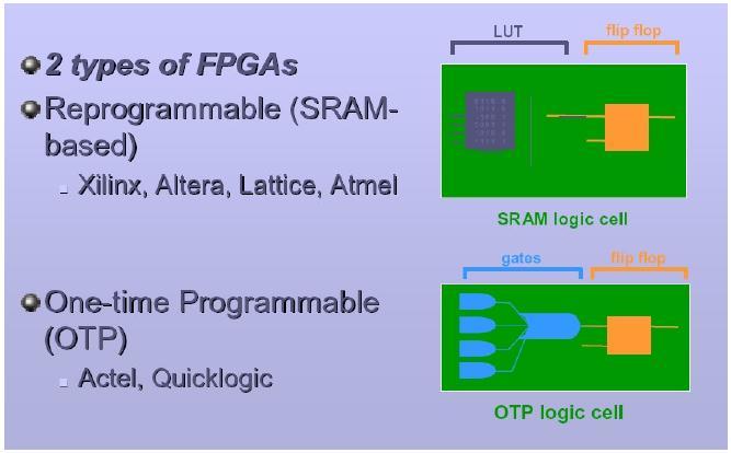
15 FPGA Types
16 FPGA advantages Highly flexible Control your design down to the individual gate level Designs can be updated without rewiring Quick turnaround during development Easy to try alternative solutions Excellent real-time performance No interrupt handler context switch overhead Fully parallel operation ABHINAV PRASAD GUPTA

17 FPGA FPGA applications:- i. DSP ii. Software-defined radio iii. Aerospace iv. Defense system v. ASIC vi. Medical Imaging vii. Computer vision viii. Speech Recognition ix. Bioinformatic x. And others. ABHINAV PRASAD GUPTA
18 Generic Array Logic (GAL): Generic array logic family consists of electrically erasable programmable devices designed by lattice semiconductor. Same logic properties as PAL but can be erased and reprogrammed. Programmed and reprogrammed using a PAL programmer It has a fixed OR array and a programmable And array the reprogrammable array is essentially a grid of conductors forming rows and columns with an electrically erasable CMOS (E2CMOS) cell at each cross point. The GAL has the programmable logic and the OLMC (Output Logic Macro cell) Logic that excludes OR gates and flip-flops.
19

20 Generic Array Logic Macrocell I/O circuit that can be configured as a registered output, a combinational output, or a dedicated input as required. Outputs can also be specified as active-high or active-low.
21 PEEL (Programmable Electrically Erasable Logic) Device : Programmable Electrically Erasable Logic Introduced by the international CMOS technology ( ICT) corporation. ICT offer the most flexible PLD solutions for lower pin count application. Include PEEL devices, PEEL array and PEEL development tool. PEEL devices are another family of devices that are intended as PAL replacements the PEEL is available in 20 pin different packages with speeds ranging from 5ns to 25ns. The PEEL architecture allows it to replace over 20 standard 20 pin PLDs (PAL, GAL, etc.)
22 Features of PEEL: 1. Speed ranging from 5ns to 25ns 2. Low Power consumption. 3. CMOS Electrically Erasable Technology. 4. Reduces development Cost 5. Flexible architecture.
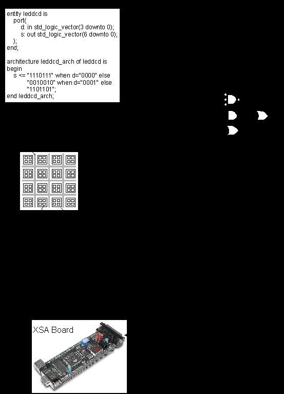
23 Design implementation using CPLD and FPGAs Implementing a logic design with the FPGA or CPLD development software usually consists of the following steps : 1. You enter a description of your logic circuit using a hardware description language (HDL) such as VHDL or Verilog. You can also draw your design using a schematic editor. 2. You use a logic synthesizer program to transform the HDL or schematic into a netlist. The netlist is just a description of the various logic gates in your design and how they are interconnected.
24 Cont.. 3. You use the implementation tools to map the logic gates and interconnections into the FPGA. The configurable logic blocks in the FPGA can be further decomposed into look-up tables that perform logic operations. The CLBs and LUTs are interwoven with various routing resources. The mapping tool collects your netlist gates into groups that fit into the LUTs and then the place & route tool assigns the gate collections to specific CLBs while opening or closing the switches in the routing matrices to connect the gates together. 4. Once the implementation phase is complete, a program extracts the state of the switches in the routing matrices and generates a bitstream where the ones and zeroes correspond to open or closed

25 Cont.. 5. The bitstream is downloaded into a physical FPGA chip (usually embedded in some larger system such as an XS Board). The electronic switches in the FPGA open or close in response to the binary bits in the bitstream. Upon completion of the downloading, the FPGA will perform the operations specified by your HDL code or schematic. You can apply input signals to the I/O pins of the FPGA to check the operation of your design.

26
Programmable Logic Devices UNIT II DIGITAL SYSTEM DESIGN
 Programmable Logic Devices UNIT II DIGITAL SYSTEM DESIGN 2 3 4 5 6 7 8 9 2 3 4 5 6 7 8 9 2 Implementation in Sequential Logic 2 PAL Logic Implementation Design Example: BCD to Gray Code Converter A B
LSN 6 Programmable Logic Devices
 LSN 6 Programmable Logic Devices Department of Engineering Technology LSN 6 What Are PLDs? Functionless devices in base form Require programming to operate The logic function of the device is programmed
ECE 331 Digital System Design
 ECE 331 Digital System Design Tristate Buffers, Read-Only Memories and Programmable Logic Devices (Lecture #17) The slides included herein were taken from the materials accompanying Fundamentals of Logic
PLAs & PALs. Programmable Logic Devices (PLDs) PLAs and PALs
 PLAs and PALs") PLAs & PALs Programmable Logic Devices (PLDs) PLAs and PALs PLAs&PALs By the late 1970s, standard logic devices were all the rage, and printed circuit boards were loaded with them. To offer the ultimate
PLAs & PALs Programmable Logic Devices (PLDs) PLAs and PALs PLAs&PALs By the late 1970s, standard logic devices were all the rage, and printed circuit boards were loaded with them. To offer the ultimate
FPGA for Complex System Implementation. National Chiao Tung University Chun-Jen Tsai 04/14/2011
 FPGA for Complex System Implementation National Chiao Tung University Chun-Jen Tsai 04/14/2011 About FPGA FPGA was invented by Ross Freeman in 1989 SRAM-based FPGA properties Standard parts Allowing multi-level
Hardware Synthesis. References
 Hardware Synthesis MidiaReshadi CE Department Science and research branch of Islamic Azad University Email: ce.srbiau@gmail.com 1 References 2 1 Chapter 1 Digital Design Using VHDL and PLDs 3 Some Definitions
Digital Electronics 27. Digital System Design using PLDs
 1 Module -27 Digital System Design 1. Introduction 2. Digital System Design 2.1 Standard (Fixed function) ICs based approach 2.2 Programmable ICs based approach 3. Comparison of Digital System Design approaches
Field Program mable Gate Arrays
 Field Program mable Gate Arrays M andakini Patil E H E P g r o u p D H E P T I F R SERC school NISER, Bhubaneshwar Nov 7-27 2017 Outline Digital electronics Short history of programmable logic devices
Evolution of Implementation Technologies. ECE 4211/5211 Rapid Prototyping with FPGAs. Gate Array Technology (IBM s) Programmable Logic
 Programmable Logic") ECE 42/52 Rapid Prototyping with FPGAs Dr. Charlie Wang Department of Electrical and Computer Engineering University of Colorado at Colorado Springs Evolution of Implementation Technologies Discrete devices:
ECE 42/52 Rapid Prototyping with FPGAs Dr. Charlie Wang Department of Electrical and Computer Engineering University of Colorado at Colorado Springs Evolution of Implementation Technologies Discrete devices:
Chapter 13 Programmable Logic Device Architectures
 Chapter 13 Programmable Logic Device Architectures Chapter 13 Objectives Selected areas covered in this chapter: Describing different categories of digital system devices. Describing different types of
CHAPTER 9 MULTIPLEXERS, DECODERS, AND PROGRAMMABLE LOGIC DEVICES
 CHAPTER 9 MULTIPLEXERS, DECODERS, AND PROGRAMMABLE LOGIC DEVICES This chapter in the book includes: Objectives Study Guide 9.1 Introduction 9.2 Multiplexers 9.3 Three-State Buffers 9.4 Decoders and Encoders
Computer Structure. Unit 2: Memory and programmable devices
 Computer Structure Unit 2: Memory and programmable devices Translated from Francisco Pérez García (fperez at us.es) by Mª Carmen Romero (mcromerot at us.es, Office G1.51, 954554324) Electronic Technology
Embedded Controller Design. CompE 270 Digital Systems - 5. Objective. Application Specific Chips. User Programmable Logic. Copyright 1998 Ken Arnold 1
 CompE 270 Digital Systems - 5 Programmable Logic Ken Arnold Objective Application Specific ICs Introduce User Programmable Logic Common Architectures Programmable Array Logic Address Decoding Example Development
DIGITAL SYSTEM FUNDAMENTALS (ECE421) DIGITAL ELECTRONICS FUNDAMENTAL (ECE4220. PROGRAMMABLE LOGIC DEVICES (PLDs)
 DIGITAL ELECTRONICS FUNDAMENTAL (ECE4220. PROGRAMMABLE LOGIC DEVICES (PLDs)") COURSE / CODE DIGITAL SYSTEM FUNDAMENTALS (ECE421) DIGITAL ELECTRONICS FUNDAMENTAL (ECE4220 PROGRAMMABLE LOGIC DEVICES (PLDs) A PLD, or programmable logic device, is an electronic component that is used
COURSE / CODE DIGITAL SYSTEM FUNDAMENTALS (ECE421) DIGITAL ELECTRONICS FUNDAMENTAL (ECE4220 PROGRAMMABLE LOGIC DEVICES (PLDs) A PLD, or programmable logic device, is an electronic component that is used
An Introduction to Programmable Logic
 Outline An Introduction to Programmable Logic 3 November 24 Transistors Logic Gates CPLD Architectures FPGA Architectures Device Considerations Soft Core Processors Design Example Quiz Semiconductors Semiconductor
Chapter 5: ASICs Vs. PLDs
 Chapter 5: ASICs Vs. PLDs 5.1 Introduction A general definition of the term Application Specific Integrated Circuit (ASIC) is virtually every type of chip that is designed to perform a dedicated task.
FPGA How do they work?
 ent FPGA How do they work? ETI135, Advanced Digital IC Design What is a FPGA? Manufacturers Distributed RAM History FPGA vs ASIC FPGA and Microprocessors Alternatives to FPGAs Anders Skoog, Stefan Granlund
FYSE420 DIGITAL ELECTRONICS. Lecture 7
 FYSE420 DIGITAL ELECTRONICS Lecture 7 1 [1] [2] [3] DIGITAL LOGIC CIRCUIT ANALYSIS & DESIGN Nelson, Nagle, Irvin, Carrol ISBN 0-13-463894-8 DIGITAL DESIGN Morris Mano Fourth edition ISBN 0-13-198924-3
Digital Integrated Circuits
 Digital Integrated Circuits Lecture 9 Jaeyong Chung Robust Systems Laboratory Incheon National University DIGITAL DESIGN FLOW Chung EPC6055 2 FPGA vs. ASIC FPGA (A programmable Logic Device) Faster time-to-market
PROGRAMMABLE MODULES SPECIFICATION OF PROGRAMMABLE COMBINATIONAL AND SEQUENTIAL MODULES
 PROGRAMMABLE MODULES SPECIFICATION OF PROGRAMMABLE COMBINATIONAL AND SEQUENTIAL MODULES. psa. rom. fpga THE WAY THE MODULES ARE PROGRAMMED NETWORKS OF PROGRAMMABLE MODULES EXAMPLES OF USES Programmable
Introduction to Field Programmable Gate Arrays
 Introduction to Field Programmable Gate Arrays Lecture 1/3 CERN Accelerator School on Digital Signal Processing Sigtuna, Sweden, 31 May 9 June 2007 Javier Serrano, CERN AB-CO-HT Outline Historical introduction.
INTRODUCTION TO FPGA ARCHITECTURE
 3/3/25 INTRODUCTION TO FPGA ARCHITECTURE DIGITAL LOGIC DESIGN (BASIC TECHNIQUES) a b a y 2input Black Box y b Functional Schematic a b y a b y a b y 2 Truth Table (AND) Truth Table (OR) Truth Table (XOR)
Programmable Logic Devices
 Programmable Logic Devices Luis Entrena, Celia López, Mario García, Enrique San Millán Universidad Carlos III de Madrid Outline Tecnologies for implementing programmable circuits Simple Programmable Logic
DIGITAL CIRCUIT LOGIC UNIT 9: MULTIPLEXERS, DECODERS, AND PROGRAMMABLE LOGIC DEVICES
 DIGITAL CIRCUIT LOGIC UNIT 9: MULTIPLEXERS, DECODERS, AND PROGRAMMABLE LOGIC DEVICES 1 Learning Objectives 1. Explain the function of a multiplexer. Implement a multiplexer using gates. 2. Explain the
ISE Design Suite Software Manuals and Help
 ISE Design Suite Software Manuals and Help These documents support the Xilinx ISE Design Suite. Click a document title on the left to view a document, or click a design step in the following figure to
Section 6. Memory Components Chapter 5.7, 5.8 Physical Implementations Chapter 7 Programmable Processors Chapter 8
 Section 6 Memory Components Chapter 5.7, 5.8 Physical Implementations Chapter 7 Programmable Processors Chapter 8 Types of memory Two major types of memory Volatile When power to the device is removed
FPGA: What? Why? Marco D. Santambrogio
 FPGA: What? Why? Marco D. Santambrogio marco.santambrogio@polimi.it 2 Reconfigurable Hardware Reconfigurable computing is intended to fill the gap between hardware and software, achieving potentially much
CS310 Embedded Computer Systems. Maeng
 1 INTRODUCTION (PART II) Maeng Three key embedded system technologies 2 Technology A manner of accomplishing a task, especially using technical processes, methods, or knowledge Three key technologies for
FPGA for Dummies. Introduc)on to Programmable Logic
on to Programmable Logic") FPGA for Dummies Introduc)on to Programmable Logic FPGA for Dummies Historical introduc)on, where we come from; FPGA Architecture: Ø basic blocks (Logic, FFs, wires and IOs); Ø addi)onal elements; FPGA
FPGA for Dummies Introduc)on to Programmable Logic FPGA for Dummies Historical introduc)on, where we come from; FPGA Architecture: Ø basic blocks (Logic, FFs, wires and IOs); Ø addi)onal elements; FPGA
EECS150 - Digital Design Lecture 6 - Field Programmable Gate Arrays (FPGAs)
") EECS150 - Digital Design Lecture 6 - Field Programmable Gate Arrays (FPGAs) September 12, 2002 John Wawrzynek Fall 2002 EECS150 - Lec06-FPGA Page 1 Outline What are FPGAs? Why use FPGAs (a short history
EECS150 - Digital Design Lecture 6 - Field Programmable Gate Arrays (FPGAs) September 12, 2002 John Wawrzynek Fall 2002 EECS150 - Lec06-FPGA Page 1 Outline What are FPGAs? Why use FPGAs (a short history
CMPE 415 Programmable Logic Devices FPGA Technology I
 Department of Computer Science and Electrical Engineering CMPE 415 Programmable Logic Devices FPGA Technology I Prof. Ryan Robucci Some slides (blue-frame) developed by Jim Plusquellic Some images credited
Outline. EECS150 - Digital Design Lecture 6 - Field Programmable Gate Arrays (FPGAs) FPGA Overview. Why FPGAs?
 FPGA Overview. Why FPGAs?") EECS150 - Digital Design Lecture 6 - Field Programmable Gate Arrays (FPGAs) September 12, 2002 John Wawrzynek Outline What are FPGAs? Why use FPGAs (a short history lesson). FPGA variations Internal logic
EECS150 - Digital Design Lecture 6 - Field Programmable Gate Arrays (FPGAs) September 12, 2002 John Wawrzynek Outline What are FPGAs? Why use FPGAs (a short history lesson). FPGA variations Internal logic
FPGAs in a Nutshell - Introduction to Embedded Systems-
 FPGAs in a Nutshell - Introduction to Embedded Systems- Dipl.- Ing. Falk Salewski Lehrstuhl Informatik RWTH Aachen salewski@informatik.rwth-aachen.de Winter term 6/7 Contents History FPGA architecture
ECEN 449 Microprocessor System Design. FPGAs and Reconfigurable Computing
 ECEN 449 Microprocessor System Design FPGAs and Reconfigurable Computing Some of the notes for this course were developed using the course notes for ECE 412 from the University of Illinois, Urbana-Champaign
Workspace for '4-FPGA' Page 1 (row 1, column 1)
") Workspace for '4-FPGA' Page 1 (row 1, column 1) Workspace for '4-FPGA' Page 2 (row 2, column 1) Workspace for '4-FPGA' Page 3 (row 3, column 1) ECEN 449 Microprocessor System Design FPGAs and Reconfigurable
Workspace for '4-FPGA' Page 1 (row 1, column 1) Workspace for '4-FPGA' Page 2 (row 2, column 1) Workspace for '4-FPGA' Page 3 (row 3, column 1) ECEN 449 Microprocessor System Design FPGAs and Reconfigurable
Terasic DE0 Field Programmable Gate Array (FPGA) Development Board
 Development Board") Lecture FPGA-01 DE0 FPGA Development Board and Quartus II 9.1 FPGA Design Software Terasic DE0 Field Programmable Gate Array (FPGA) Development Board 1 May 16, 2013 3 Layout and Components of DE0 May 16,
Lecture FPGA-01 DE0 FPGA Development Board and Quartus II 9.1 FPGA Design Software Terasic DE0 Field Programmable Gate Array (FPGA) Development Board 1 May 16, 2013 3 Layout and Components of DE0 May 16,
Field Programmable Gate Array (FPGA)
") Field Programmable Gate Array (FPGA) Lecturer: Krébesz, Tamas 1 FPGA in general Reprogrammable Si chip Invented in 1985 by Ross Freeman (Xilinx inc.) Combines the advantages of ASIC and uc-based systems
Field Programmable Gate Array (FPGA) Lecturer: Krébesz, Tamas 1 FPGA in general Reprogrammable Si chip Invented in 1985 by Ross Freeman (Xilinx inc.) Combines the advantages of ASIC and uc-based systems
Lecture (1) Introduction to FPGA. 1. The History of Programmable Logic
 Introduction to FPGA. 1. The History of Programmable Logic") Lecture (1) Introduction to FPGA 1. The History of Programmable Logic By the late 1970s, standard logic devices were all the rage, and printed circuit boards were loaded with them. Then someone asked,
Lecture (1) Introduction to FPGA 1. The History of Programmable Logic By the late 1970s, standard logic devices were all the rage, and printed circuit boards were loaded with them. Then someone asked,
New Logic Module for secured FPGA based system
 International Journal of Electronics and Communication Engineering. ISSN 0974-2166 Volume 5, Number 4 (2012), pp. 533-543 International Research Publication House http://www.irphouse.com New Logic Module
Memory and Programmable Logic
 Digital Circuit Design and Language Memory and Programmable Logic Chang, Ik Joon Kyunghee University Memory Classification based on functionality ROM : Read-Only Memory RWM : Read-Write Memory RWM NVRWM
Introduction to Digital Logic Missouri S&T University CPE 2210 Hardware Implementations
 Introduction to Digital Logic Missouri S&T University CPE 2210 Hardware Implementations Egemen K. Çetinkaya Egemen K. Çetinkaya Department of Electrical & Computer Engineering Missouri University of Science
Chapter 10: Design Options of Digital Systems
 Chapter 10: Design Options of Digital Systems Prof. Ming-Bo Lin Department of Electronic Engineering National Taiwan University of Science and Technology Digital System Designs and Practices Using Verilog
Copyright by Syed Ashad Mustufa Younus Copyright by Syed Ashad Mustufa Younus
 Copyright by Syed Ashad Mustufa Younus Copyright by Syed Ashad Mustufa Younus Microcontroller & Applications Week 2 Instructor: Syed Ashad Mustufa Younus HP: +92 (0) 300 240 8943 Email: :sashad@iqra.edu.pks
RTL Coding General Concepts
 RTL Coding General Concepts Typical Digital System 2 Components of a Digital System Printed circuit board (PCB) Embedded d software microprocessor microcontroller digital signal processor (DSP) ASIC Programmable
Memory and Programmable Logic
 Memory and Programmable Logic Mano & Ciletti Chapter 7 By Suleyman TOSUN Ankara University Outline RAM Memory decoding Error detection and correction ROM Programmable Logic Array (PLA) Programmable Array
Design Methodologies and Tools. Full-Custom Design
 Design Methodologies and Tools Design styles Full-custom design Standard-cell design Programmable logic Gate arrays and field-programmable gate arrays (FPGAs) Sea of gates System-on-a-chip (embedded cores)
2001 by X Engineering Software Systems Corp., Apex, North Carolina 27502
 2001 by X Engineering Software Systems Corp., Apex, North Carolina 27502 All rights reserved. No part of this text may be reproduced, in any form or by any means, without permission in writing from the
Topics. Midterm Finish Chapter 7
 Lecture 9 Topics Midterm Finish Chapter 7 ROM (review) Memory device in which permanent binary information is stored. Example: 32 x 8 ROM Five input lines (2 5 = 32) 32 outputs, each representing a memory
Copyright 2011 R.S.R. Electronics, Inc. All rights reserved. 04/11. Ver. 1.0web
 For XILINX WebPack Copyright 2011 R.S.R. Electronics, Inc. All rights reserved. 04/11 Ver. 1.0web 1 Table of Contents 1.0 INTRODUCTION...3 2.0 GENERAL DESCRIPTION...5 3.0 BRIEF DESCRIPTION Of PLDT-3 BOARD...6
Lecture 13: Memory and Programmable Logic
 Lecture 13: Memory and Programmable Logic Syed M. Mahmud, Ph.D ECE Department Wayne State University Aby K George, ECE Department, Wayne State University Contents Introduction Random Access Memory Memory
FPGA Based Digital Design Using Verilog HDL
 FPGA Based Digital Design Using Course Designed by: IRFAN FAISAL MIR ( Verilog / FPGA Designer ) irfanfaisalmir@yahoo.com * Organized by Electronics Division Integrated Circuits Uses for digital IC technology
Using XILINX WebPACK Software to Create CPLD Designs
 Introduction to WebPACK Using XILINX WebPACK Software to Create CPLD Designs RELEASE DATE: 10/24/1999 All XS-prefix product designations are trademarks of XESS Corp. All XC-prefix product designations
Programmable Logic Devices (PLDs)
") Programmable Logic Devices (PLDs) 212: Digital Design I, week 13 PLDs basically store binary information in a volatile/nonvolatile device. Data is specified by designer and physically inserted (Programmed)
Programmable Logic Devices (PLDs) 212: Digital Design I, week 13 PLDs basically store binary information in a volatile/nonvolatile device. Data is specified by designer and physically inserted (Programmed)
Lecture 7. Standard ICs FPGA (Field Programmable Gate Array) VHDL (Very-high-speed integrated circuits. Hardware Description Language)
 VHDL (Very-high-speed integrated circuits. Hardware Description Language)") Standard ICs FPGA (Field Programmable Gate Array) VHDL (Very-high-speed integrated circuits Hardware Description Language) 1 Standard ICs PLD: Programmable Logic Device CPLD: Complex PLD FPGA: Field Programmable
Standard ICs FPGA (Field Programmable Gate Array) VHDL (Very-high-speed integrated circuits Hardware Description Language) 1 Standard ICs PLD: Programmable Logic Device CPLD: Complex PLD FPGA: Field Programmable
MEMORY AND PROGRAMMABLE LOGIC
 MEMORY AND PROGRAMMABLE LOGIC Memory is a device where we can store and retrieve information It can execute a read and a write Programmable Logic is a device where we can store and retrieve information
Follow-up question: now, comment on what each of these acronyms actually means, going beyond a mere recitation of the definition.
 Question 1 Define the following acronyms as they apply to digital logic circuits: ASIC PAL PLA PLD CPLD FPGA file 03041 Answer 1 ASIC: Application-Specific Integrated Circuit PAL: Programmable Array Logic
Basic FPGA Architectures. Actel FPGAs. PLD Technologies: Antifuse. 3 Digital Systems Implementation Programmable Logic Devices
 3 Digital Systems Implementation Programmable Logic Devices Basic FPGA Architectures Why Programmable Logic Devices (PLDs)? Low cost, low risk way of implementing digital circuits as application specific
Field Programmable Gate Array
 Field Programmable Gate Array System Arch 27 (Fire Tom Wada) What is FPGA? System Arch 27 (Fire Tom Wada) 2 FPGA Programmable (= reconfigurable) Digital System Component Basic components Combinational
Outline. Field Programmable Gate Arrays. Programming Technologies Architectures. Programming Interfaces. Historical perspective
 Outline Field Programmable Gate Arrays Historical perspective Programming Technologies Architectures PALs, PLDs,, and CPLDs FPGAs Programmable logic Interconnect network I/O buffers Specialized cores Programming
Very Large Scale Integration (VLSI)
") Very Large Scale Integration (VLSI) Lecture 6 Dr. Ahmed H. Madian Ah_madian@hotmail.com Dr. Ahmed H. Madian-VLSI 1 Contents FPGA Technology Programmable logic Cell (PLC) Mux-based cells Look up table PLA
Very Large Scale Integration (VLSI) Lecture 6 Dr. Ahmed H. Madian Ah_madian@hotmail.com Dr. Ahmed H. Madian-VLSI 1 Contents FPGA Technology Programmable logic Cell (PLC) Mux-based cells Look up table PLA
Design Methodologies. Full-Custom Design
 Design Methodologies Design styles Full-custom design Standard-cell design Programmable logic Gate arrays and field-programmable gate arrays (FPGAs) Sea of gates System-on-a-chip (embedded cores) Design
Configurable Embedded Systems: Using Programmable Logic to Compress Embedded System Design Cycles
 Class 330 Configurable Embedded Systems: Using Programmable Logic to Compress Embedded System Design Cycles Steven Knapp (sknapp) Arye Ziklik (arye) Triscend Corporation www.triscend.com Copyright 1998,
LSN 1 Digital Design Flow for PLDs
 LSN 1 Digital Design Flow for PLDs ECT357 Microprocessors I Department of Engineering Technology LSN 1 Programmable Logic Devices Functionless devices in base form Require programming to operate The logic
FPGA. Logic Block. Plessey FPGA: basic building block here is 2-input NAND gate which is connected to each other to implement desired function.
 FPGA Logic block of an FPGA can be configured in such a way that it can provide functionality as simple as that of transistor or as complex as that of a microprocessor. It can used to implement different
Design Progression With VHDL Helps Accelerate The Digital System Designs
 Fourth LACCEI International Latin American and Caribbean Conference for Engineering and Technology (LACCET 2006) Breaking Frontiers and Barriers in Engineering: Education, Research and Practice 21-23 June
Introduction to WebPACK 3.1. Using XILINX WebPACK Software to Create CPLD Designs
 Introduction to WebPACK 3.1 Using XILINX WebPACK Software to Create CPLD Designs RELEASE DATE: 8/28/2000 All XS-prefix product designations are trademarks of XESS Corp. All XC-prefix product designations
Programmable logic technology
 Programmable logic technology This worksheet and all related files are licensed under the Creative Commons Attribution License, version 1.0. To view a copy of this license, visit http://creativecommons.org/licenses/by/1.0/,
Unit 6 1.Random Access Memory (RAM) Chapter 3 Combinational Logic Design 2.Programmable Logic
 Chapter 3 Combinational Logic Design 2.Programmable Logic") EE 200: Digital Logic Circuit Design Dr Radwan E Abdel-Aal, COE Unit 6.Random Access Memory (RAM) Chapter 3 Combinational Logic Design 2. Logic Logic and Computer Design Fundamentals Part Implementation
EE 200: Digital Logic Circuit Design Dr Radwan E Abdel-Aal, COE Unit 6.Random Access Memory (RAM) Chapter 3 Combinational Logic Design 2. Logic Logic and Computer Design Fundamentals Part Implementation
Memory and Programmable Logic
 Memory and Programmable Logic Memory units allow us to store and/or retrieve information Essentially look-up tables Good for storing data, not for function implementation Programmable logic device (PLD),
EECS150, Fall 2004, Midterm 1, Prof. Culler. Problem 1 (15 points) 1.a. Circle the gate-level circuits that DO NOT implement a Boolean AND function.
 1.a. Circle the gate-level circuits that DO NOT implement a Boolean AND function.") Problem 1 (15 points) 1.a. Circle the gate-level circuits that DO NOT implement a Boolean AND function. 1.b. Show that a 2-to-1 MUX is universal (i.e. that any Boolean expression can be implemented with
Problem 1 (15 points) 1.a. Circle the gate-level circuits that DO NOT implement a Boolean AND function. 1.b. Show that a 2-to-1 MUX is universal (i.e. that any Boolean expression can be implemented with
Programmable Logic Devices FPGA Architectures II CMPE 415. Overview This set of notes introduces many of the features available in the FPGAs of today.
 Overview This set of notes introduces many of the features available in the FPGAs of today. The majority use SRAM based configuration cells, which allows fast reconfiguation. Allows new design ideas to
Experiment 3. Digital Circuit Prototyping Using FPGAs
 Experiment 3. Digital Circuit Prototyping Using FPGAs Masud ul Hasan Muhammad Elrabaa Ahmad Khayyat Version 151, 11 September 2015 Table of Contents 1. Objectives 2. Materials Required 3. Background 3.1.
Introduction to WebPACK 4.1 for FPGAs. Using Xilinx WebPACK Software to Create FPGA Designs for the XSA Board
 Introduction to WebPACK 4.1 for FPGAs Using Xilinx WebPACK Software to Create FPGA Designs for the XSA Board Release date: 10/29/2001 All XS-prefix product designations are trademarks of XESS Corp. All
ECE U530 Digital Hardware Synthesis. What is the course about?
 ECE U530 Digital Hardware Synthesis Prof. Miriam Leeser mel@coe.neu.edu Sept 6, 2006 Lecture 1: Overview Organization What is an ASIC? Why FPGAs? Hardware Description Languages and VHDL ECE U530 F06 What
ELCT 912: Advanced Embedded Systems
 Advanced Embedded Systems Lecture 2: Memory and Programmable Logic Dr. Mohamed Abd El Ghany, Memory Random Access Memory (RAM) Can be read and written Static Random Access Memory (SRAM) Data stored so
FPGA Design Flow 1. All About FPGA
 FPGA Design Flow 1 In this part of tutorial we are going to have a short intro on FPGA design flow. A simplified version of FPGA design flow is given in the flowing diagram. FPGA Design Flow 2 FPGA_Design_FLOW
Today. Comments about assignment Max 1/T (skew = 0) Max clock skew? Comments about assignment 3 ASICs and Programmable logic Others courses
 Max clock skew? Comments about assignment 3 ASICs and Programmable logic Others courses") Today Comments about assignment 3-43 Comments about assignment 3 ASICs and Programmable logic Others courses octor Per should show up in the end of the lecture Mealy machines can not be coded in a single
Today Comments about assignment 3-43 Comments about assignment 3 ASICs and Programmable logic Others courses octor Per should show up in the end of the lecture Mealy machines can not be coded in a single
Programmable Logic. Any other approaches?
 Programmable Logic So far, have only talked about PALs (see 22V10 figure next page). What is the next step in the evolution of PLDs? More gates! How do we get more gates? We could put several PALs on one
CONTENTS CHAPTER 1: NUMBER SYSTEM. Foreword...(vii) Preface... (ix) Acknowledgement... (xi) About the Author...(xxiii)
 Preface... (ix) Acknowledgement... (xi) About the Author...(xxiii)") CONTENTS Foreword...(vii) Preface... (ix) Acknowledgement... (xi) About the Author...(xxiii) CHAPTER 1: NUMBER SYSTEM 1.1 Digital Electronics... 1 1.1.1 Introduction... 1 1.1.2 Advantages of Digital Systems...
CONTENTS Foreword...(vii) Preface... (ix) Acknowledgement... (xi) About the Author...(xxiii) CHAPTER 1: NUMBER SYSTEM 1.1 Digital Electronics... 1 1.1.1 Introduction... 1 1.1.2 Advantages of Digital Systems...
SYSTEM DESIGNING AND MODELLING USING FPGA
 INTERNATIONAL JOURNAL OF ELECTRONICS AND COMMUNICATION ENGINEERING & TECHNOLOGY (IJECET) International Journal of Electronics and Communication Engineering & Technology (IJECET), ISSN 0976 ISSN 0976 6464(Print)
Design Methodologies
 Design Methodologies 1981 1983 1985 1987 1989 1991 1993 1995 1997 1999 2001 2003 2005 2007 2009 Complexity Productivity (K) Trans./Staff - Mo. Productivity Trends Logic Transistor per Chip (M) 10,000 0.1
What is Xilinx Design Language?
 Bill Jason P. Tomas University of Nevada Las Vegas Dept. of Electrical and Computer Engineering What is Xilinx Design Language? XDL is a human readable ASCII format compatible with the more widely used
FPGA Implementations
 FPGA Implementations Smith Text: Chapters 4-8 Online version at: http://www10.edacafe.com/book/asic/asics.php Topic outline Chapter 4 Programmable ASIC technologies Chapter 5 Programmable logic cells Chapter
PROGRAMMABLE LOGIC DEVICES
 PROGRAMMABLE LOGIC DEVICES Programmable logic devices (PLDs) are used for designing logic circuits. PLDs can be configured by the user to perform specific functions. The different types of PLDs available
Purdue IMPACT 2015 Edition by D. G. Meyer. Introduction to Digital System Design. Module 2 Combinational Logic Circuits
 Purdue IMPACT 25 Edition by D. G. Meyer Introduction to Digital System Design Module 2 Combinational Logic Circuits Glossary of Common Terms DISCRETE LOGIC a circuit constructed using small-scale integrated
Graduate course on FPGA design
 History of and programmable logic February 15, 2010 History of and programmable logic History of and programmable logic History of and programmable logic Course planning Lectures Laboration 4 HP for actively
Programmable Logic Devices. PAL & Jedec Programming
 Programmable Logic Devices PAL & Jedec Programming PAL Devices: PAL = Programmable Array Logic The PAL naming is trademark of the AMD Firm, but Lattice also use these circuits. The PAL device is a PLD
CMPE 415 Programmable Logic Devices Introduction
 Department of Computer Science and Electrical Engineering CMPE 415 Programmable Logic Devices Introduction Prof. Ryan Robucci What are FPGAs? Field programmable Gate Array Typically re programmable as
UNIT V (PROGRAMMABLE LOGIC DEVICES)
") UNIT V (PROGRAMMABLE LOGIC DEVICES) Introduction There are two types of memories that are used in digital systems: Random-access memory(ram): perform both the write and read operations. Read-only memory(rom):
UNIT V (PROGRAMMABLE LOGIC DEVICES) Introduction There are two types of memories that are used in digital systems: Random-access memory(ram): perform both the write and read operations. Read-only memory(rom):
Introduction to Programmable Logic Devices (Class 7.2 2/28/2013)
") Introduction to Programmable Logic Devices (Class 7.2 2/28/2013) CSE 2441 Introduction to Digital Logic Spring 2013 Instructor Bill Carroll, Professor of CSE Today s Topics Complexity issues Implementation
Introduction to Programmable Logic Devices (Class 7.2 2/28/2013) CSE 2441 Introduction to Digital Logic Spring 2013 Instructor Bill Carroll, Professor of CSE Today s Topics Complexity issues Implementation
Actel s SX Family of FPGAs: A New Architecture for High-Performance Designs
 Actel s SX Family of FPGAs: A New Architecture for High-Performance Designs A Technology Backgrounder Actel Corporation 955 East Arques Avenue Sunnyvale, California 94086 April 20, 1998 Page 2 Actel Corporation
Programmable Logic Devices Introduction CMPE 415. Programmable Logic Devices
 Instructor: Professor Jim Plusquellic Programmable Logic Devices Text: The Design Warrior s Guide to FPGAs, Devices, Tools and Flows, Clive "Max" Maxfield, ISBN: 0-7506-7604-3 Modeling, Synthesis and Rapid
Introduction to WebPACK 4.1 for CPLDs. Using Xilinx WebPACK Software to Create CPLD Designs for the XS95 Board
 Introduction to WebPACK 4.1 for CPLDs Using Xilinx WebPACK Software to Create CPLD Designs for the XS95 Board Release date: 10/29/2001 All XS-prefix product designations are trademarks of XESS Corp. All
Read-only memory Implementing logic with ROM Programmable logic devices Implementing logic with PLDs Static hazards
 Points Addressed in this Lecture Lecture 7: ROM Programmable Logic Devices Professor Peter Cheung Department of EEE, Imperial College London Read-only memory Implementing logic with ROM Programmable logic
Usable gates 600 1,250 2,500 5,000 10,000 Macrocells Logic array blocks Maximum user I/O
 MAX 3000A Programmable Logic Device Family June 2006, ver. 3.5 Data Sheet Features... High performance, low cost CMOS EEPROM based programmable logic devices (PLDs) built on a MAX architecture (see Table
Chapter 2. FPGA and Dynamic Reconfiguration ...
 Chapter 2 FPGA and Dynamic Reconfiguration... This chapter will introduce a family of silicon devices, FPGAs exploring their architecture. This work is based on these particular devices. The chapter will
Second Edition Programmable Logic Design Quick Start Hand Book
 Second Edition Programmable Logic Design Quick Start Hand Book By Karen Parnell & Nick Mehta January 2002 ABSTRACT Whether you design with discrete logic, base all of your designs on microcontrollers,
Synthesis of VHDL Code for FPGA Design Flow Using Xilinx PlanAhead Tool
 Synthesis of VHDL Code for FPGA Design Flow Using Xilinx PlanAhead Tool Md. Abdul Latif Sarker, Moon Ho Lee Division of Electronics & Information Engineering Chonbuk National University 664-14 1GA Dekjin-Dong
SPLD & CPLD architectures
 Module: Electronics & Telecomunication, 5rd year Hardware Acceleration of Telecommunication Protocols SPLD & CPLD architectures 1 PLD devices classification Source: Dataquest Logic Standard Logic ASIC
TLL5000 Electronic System Design Base Module. Getting Started Guide, Ver 3.4
 TLL5000 Electronic System Design Base Module Getting Started Guide, Ver 3.4 COPYRIGHT NOTICE The Learning Labs, Inc. ( TLL ) All rights reserved, 2008 Reproduction in any form without permission is prohibited.