UNIT 3 THE 8051-REAL WORLD INTERFACING
|
|
|
- Martha Jackson
- 5 years ago
- Views:
Transcription
1 UNIT 3 THE 8051-REAL WORLD INTERFACING
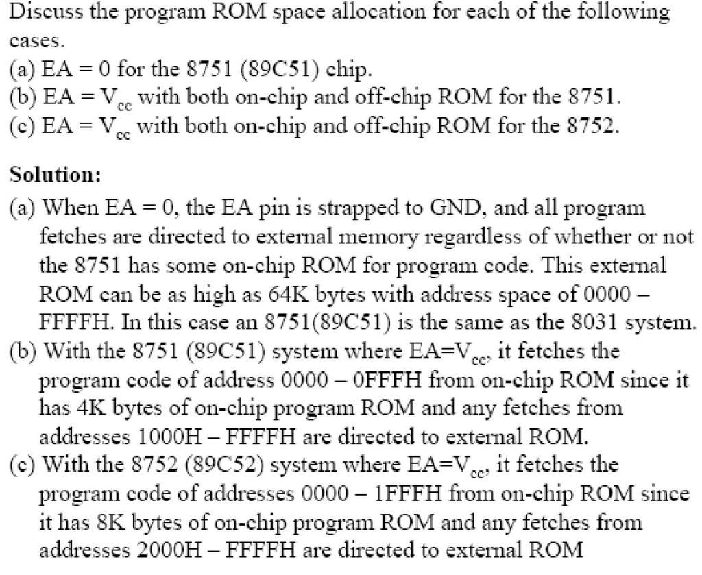
2 8031/51 INTERFACING TO EXTERNAL MEMORY The number of bits that a semiconductor memory chip can store is called chip capacity It can be in units of Kbits (kilobits), Mbits (megabits), and so on This must be distinguished from the storage capacity of computer systems While the memory capacity of a memory IC chip is always given bits, the memory capacity of a computer system is given in bytes 16M memory chip 16 megabits A computer comes with 16M memory 16 megabytes Memory chips are organized into a number of locations within the IC Each location can hold 1 bit, 4 bits, 8 bits, or even 16 bits, depending on how it is designed internally The number of locations within a memory IC depends on the address pins The number of bits that each location can hold is always equal to the number of data pins To summarize A memory chip contain 2x location, where x is the number of address pins Each location contains y bits, where y is the number of data pins on the chip The entire chip will contain 2x y bits One of the most important characteristics of a memory chip is the speed at which its data can be accessed To access the data, the address is presented to the address pins, the READ pin is activated, and after a certain amount of time has elapsed, the data shows up at the data pins The shorter this elapsed time, the better, and consequently, the more expensive the memory chip The speed of the memory chip is commonly referred to as its access time 2
3 ROM is a type of memory that does not lose its contents when the power is turned off ROM is also called nonvolatile memory There are different types of read-only memory PROM EPROM EEPROM Flash EPROM Mask ROM The CPU provides the address of the data desired, but it is the job of the decoding circuitry to locate the selected memory block Memory chips have one or more pins called CS (chip select), which must be activated for the memory s contents to be accessed Sometimes the chip select is also referred to as chip enable (CE) In connecting a memory chip to the CPU, note the following points The data bus of the CPU is connected directly to the data pins of the memory chip Control signals RD (read) and WR (memory write) from the CPU are connected to the OE (output enable) and WE (write enable) pins of the memory chip In the case of the address buses, while the lower bits of the address from the CPU go directly to the memory chip address pins, the upper ones are used to activate the CS pin of the memory chip Normally memories are divided into blocks and the output of the decoder selects a given memory block Using simple logic gates Using the 74LS138 Using programmable logics The simplest way of decoding circuitry is the use of NAND or other gates The fact that the output of a NAND gate is active low, and that the CS pin is also active low makes them a perfect match 3

4 This is one of the most widely used address decoders The 3 inputs A, B, and C generate 8 activelow outputs Y0 Y7 Each Y output is connected to CS of a memory chip, allowing control of 8 memory blocks by a single 74LS138 In the 74LS138, where A, B, and C select which output is activated, there are three additional inputs, G2A, G2B, and G1 G2A and G2B are both active low, and G1 is active high If any one of the inputs G1, G2A, or G2B is not connected to an address signal, they must be activated permanently either by Vcc or ground, depending on the activation level 4
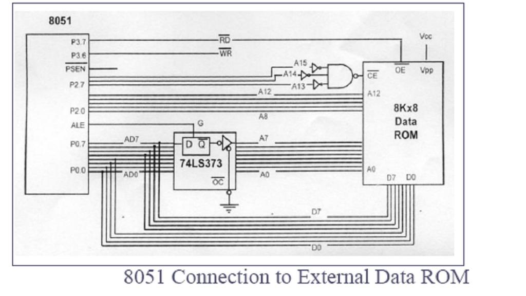
5 Other widely used decoders are programmable logic chips such as PAL and GAL chips One disadvantage of these chips is that one must have access to a PAL/GAL software and burner, whereas the 74LS138 needs neither of these The advantage of these chips is that they are much more versatile since they can be programmed for any combination of address ranges The 8031 chip is a ROMless version of the 8051 It is exactly like any member of the 8051 family as far as executing the instructions and features are concerned, but it has no on-chip ROM To make the 8031 execute 8051 code, it must be connected to external ROM memory containing the program code 8031 is ideal for many systems where the on-chip ROM of 8051 is not sufficient, since it allows the program size to be as large as 64K bytes For 8751/89C51/DS5000- based system, we connected the EA pin to Vcc to indicate that the program code is stored in the microcontroller s on-chip ROM To indicate that the program code is stored in external ROM, this pin must be connected to GND Since the PC (program counter) of the 8031/51 is 16-bit, it is capable of accessing up to 64K bytes of program code In the 8031/51, port 0 and port 2 provide the 16-bit address to access external memory P0 provides the lower 8 bit address A0 A7, and P2 provides the upper 8 bit address A8 A15 P0 is also used to provide the 8-bit data bus D0 D7 P0.0 P0.7 are used for both the addressand data paths address/data multiplexing ALE (address latch enable) pin is an output pin for 8031/51 ALE = 0, P0 is used for data path ALE = 1, P0 is used for address path 74LS373 D Latch To extract the address from the P0 pins we connect P0 to a 74LS373 and use the ALE pin to latch the address Normally ALE = 0, and P0 is used as a data bus, sending data out or bringing data in Whenever the 8031/51 wants to use P0 as an address bus, it puts the addresses A0 A7 on the P0 pins and activates ALE = 1 5


6 PSEN (program store enable) signal is an output signal for the 8031/51 microcontroller and must be connected to the OE pin of a ROM containing the program code It is important to emphasize the role of EA and PSEN when connecting the 8031/51 to external ROM When the EA pin is connected to GND, the 8031/51 fetches opcode from external ROM by using PSEN The connection of the PSEN pin to the OE pin of ROM In systems based on the 8751/89C51/ DS5000 where EA is connected to Vcc, these chips do not activate the PSEN pin This indicates that the on-chip ROM contains program code Connection to External Program ROM 6
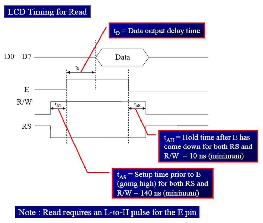
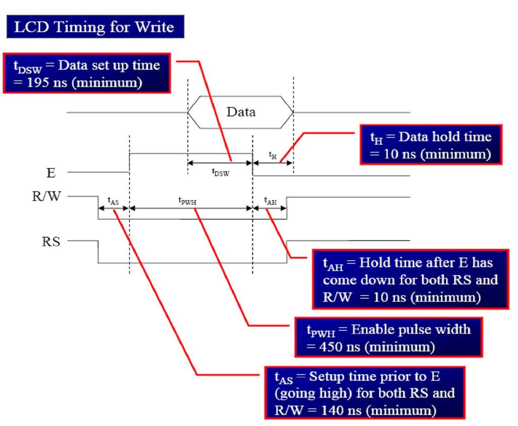
7 7


8 Show the design of an 8031-based system with 8K bytes of program ROM and 8K bytes of data ROM. 8
9 speed control of a stepper motor The requirement is to use a microcontroller to drive a stepper motor in both forward and reverse directions of shaft rotation and to implement a two-speed (fast and slow) arrangement. Switches are to be used to produce the two speeds and effect a reversal of shaft rotation. A possible arrangement is shown in the block diagram, which uses a P89C664 microcontroller. 9
10 Generally a stepper motor has four sets of coils. One end of each coil may be connected together and then connected to DCsu pply. The remaining four ends may be driven through transistors either separately or in integrated circuit form. A four-bit code sequence continuously applied to the drive circuit from the microcontroller port causes the motor shaft to rotate in angular steps. Cheap (e.g. 12) stepper motors have step angles of 7.5 degrees whereas more expensive (e.g. 45) motors have step angles of 1.8 degrees. Step resolution and turning force (i.e. torque) may be improved by using a step-down gearbox. The stepping code sequence may be obtained from the motor manufacturer or distributor. The program in this example uses a common fourstep sequence of A that, if sent continuously, would cause the motor shaft to rotate. Figure 7.8 shows the driving signals from the port pins. Sending the code in reverse A causes the motor shaft rotation to reverse. The rotation speed depends on the delay each step is held for. Details of a suitable drive circuit are shown in Figure 7.9. The transistors (TR) must be chosen to easily handle the coil current. If the value of coil current is not given by the motor supplier then it is possible to measure the coil resistance with a multimeter (a typical value would be 15 ohms). Dividing Vcc by the coil resistance gives a good estimate of the coil current; double this value and select a transistor that has this current as its maximum-rated value. In this way the transistors will not run hot. The value of resistor R is chosen to control the input current of the transistor. The transistor current ratio is given in component catalogues as hfe, which is device forward current gain in commonemitter mode. In this circuit hfe is basically the coil current divided by the input current to the transistor. Thus the transistor input current is: input current=(coil current)=hfe The 74LS04 logic gate comprises eight inverter buffer circuits. Using two in series will restore the voltage level at the input to resistor R to the same value as the output from the relevant port pin. The voltage from the 74LS04 logic gate to turn on the transistor is 5 V. The voltage input to the transistor on the other side of the resistor is approximately 0.7 V; so the voltage difference across the resistor R is (5 _ 0:7)V ¼ 4:3V 10
11 The resistor value is given by: R ¼ ðvoltage across the resistorþ/input current R ¼ ð4:3 _ hfeþ=ðcoil currentþ A logic 1 (5 V) from the microcontroller port pin is applied through the two inverter gates of the 74LS04 to the resistor R. This sets up 0.7V to the transistor base that causes the transistor to behave as an electronic switch, turning the device on and allowing current to flow through the coil. The logic gates act as a buffer ensuring that the microcontroller port pin is not current loaded. The diodes D reduce the large induced voltages caused when the current is suddenly switched on or off. TIMER VALUES FOR ROTATION SPEED Consider a 7.5 degree stepper motor having a step sequence of A Assume it is desired to make the shaft rotate at 60 revolutions per minute or one revolution every second. 360/7:5 ¼ 48 steps in a revolution and the program action will basically be step-delay; so this means 48 delays¼one revolution. 48 delays ¼ 1 s 1 delay ¼ ð1=48þ s ¼ 20:833 ms 11
 Write a program to send 55H and AAH to all ports continuously.")
12 8031/51 INTERFACING WITH THE 8255 (a) Find the I/O port addresses assigned to ports A, B, C, and the control register. (b) Program the 8255 for ports A, B, and C to be output ports. (c) Write a program to send 55H and AAH to all ports continuously. Solution (a) The base address for the 8255 is as follows: (b) The control byte (word) for all ports as output is 80H as seen in 12
13 Example For Figure above. 13
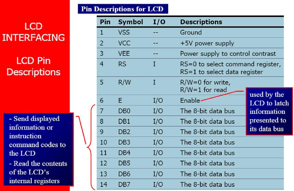
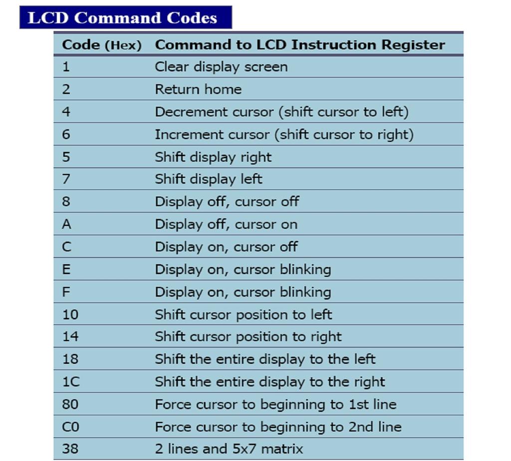
14 (a) Find the I/O port addresses assigned to ports A, B, C, and the control register. (b) Find the control byte for PA = in, PB = out, PC = out. (c) Write a program to get data from PA and send it to both B and C. Solution: (a) Assuming all the unused bits are 0s, the base port address for 8255 is 1000H. Therefore we have: 1000H PA 1001H PB 1002H PC 1003H Control register (b) The control word is , or 90H. LCD AND KEYBOARD INTERFACING LCD is finding widespread use replacing LEDs The declining prices of LCD The ability to display numbers, characters,and graphics Incorporation of a refreshing controller into the LCD, thereby relieving the CPU of the task of refreshing the LCD Ease of programming for characters and graphics 14
15 15
16 16

17 Keyboards are organized in a matrix of rows and columns The CPU accesses both rows and columns through ports Therefore, with two 8-bit ports, an 8 x 8 matrix of keys can be connected to a microprocessor When a key is pressed, a row and a column make a contact Otherwise, there is no connection between rows and columns In IBM PC keyboards, a single microcontroller takes care of hardware and software interfacing A 4x4 matrix connected to two ports The rows are connected to an output port and the columns are connected to an input port It is the function of the microcontroller to scan the keyboard continuously to detect and identify the key pressed To detect a pressed key, the microcontroller grounds all rows by providing 0 to the output latch, then it reads the columns If the data read from columns is D3 D0 = 1111, no key has been pressed and the process continues till key press is detected If one of the column bits has a zero, this means that a key press has occurred For example, if D3 D0 = 1101, this means that a key in the D1 column has been pressed After detecting a key press, microcontroller Starting with the top row, the microcontroller grounds it by providing a low to row D0 only 17
18 It reads the columns, if the data read is all 1s, no key in that row is activated and the process is moved to the next row It grounds the next row, reads the columns, and checks for any zero This process continues until the row is identified After identification of the row in which the key has been pressed Find out which column the pressed key belongs to Program 12-4 for detection and identification of key activation goes through the following stages: 1. To make sure that the preceding key has been released, 0s are output to all rows at once, and the columns are read and checked repeatedly until all the columns are high When all columns are found to be high, the program waits for a short amount of time before it goes to the next stage of waiting for a key to be pressed To see if any key is pressed, the columns are scanned over and over in an infinite loop until one of them has a 0 on it Remember that the output latches connected to rows still have their initial zeros (provided in stage 1), making them grounded 18

19 After the key press detection, it waits 20 ms for the bounce and then scans the columns again (a) it ensures that the first key press detection was not an erroneous one due a spike noise (b) the key press. If after the 20-ms delay the key is still pressed, it goes back into the loop to detect a real key press To detect which row key press belongs to, it grounds one row at a time, reading the columns each time If it finds that all columns are high, this means that the key press cannot belong to that row Therefore, it grounds the next row and continues until it finds the row the key press belongs to Upon finding the row that the key press belongs to, it sets up the starting address for the look-up table holding the scan codes (or ASCII) for that row 4. To identify the key press, it rotates the column bits, one bit at a time, into the carry flag and checks to see if it is low Upon finding the zero, it pulls out the ASCII code for that key from the look-up table otherwise, it increments the pointer to point to the next Element of the look-up table 19
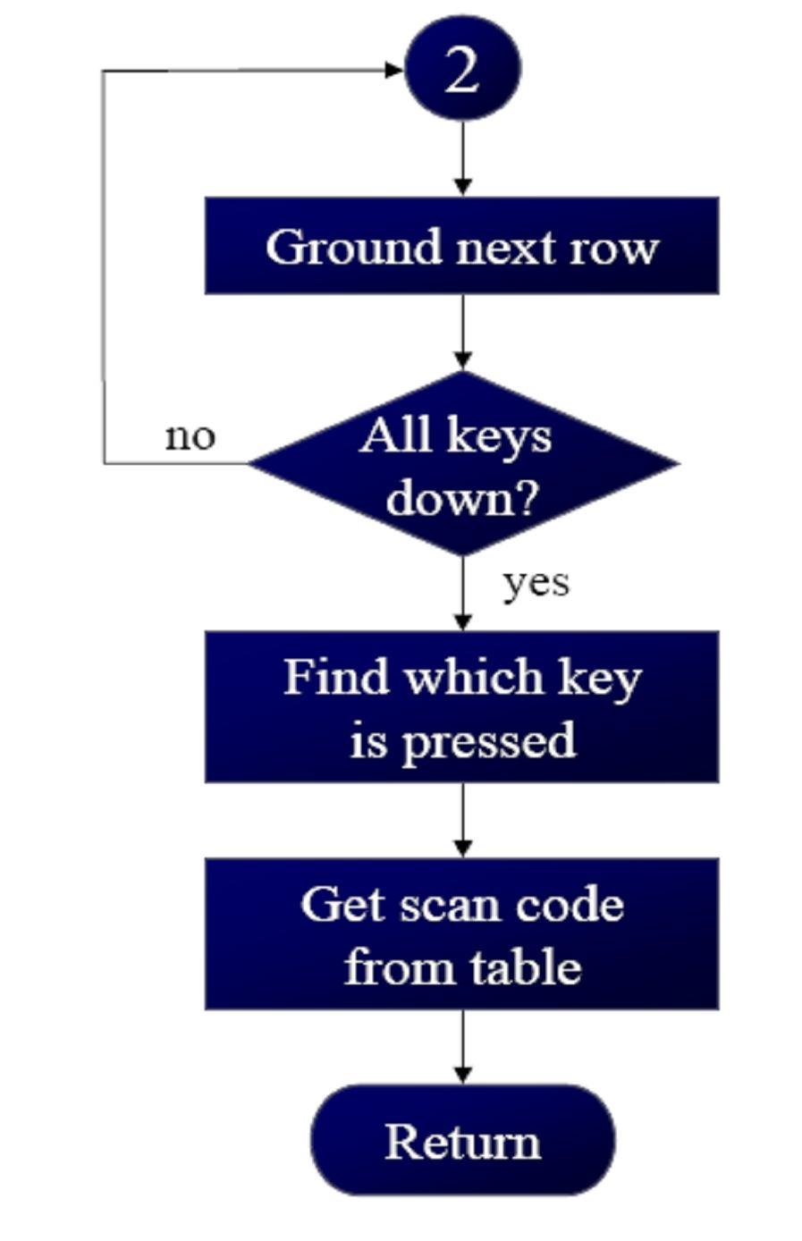
20 20
21 21
 signals using a device called a transducer, or sensor We need an analog-to-digital converter to translate the analog signals to digital numbers, so")
22 INTERFACING ADC ADCs (analog-to-digital converters) are among the most widely used devices for data acquisition A physical quantity, like temperature, pressure, humidity, and velocity, etc., is converted to electrical (voltage, current) signals using a device called a transducer, or sensor We need an analog-to-digital converter to translate the analog signals to digital numbers, so microcontroller can read them ADC804 IC is an analog-to-digital converter It works with +5 volts and has a resolution of 8 bits Conversion time is another major factor in judging an ADC Conversion time is defined as the time it takes the ADC to convert the analog input to a digital (binary) number In ADC804 conversion time varies depending on the clocking signals applied to CLK R and CLK IN pins, but it cannot be faster than 110 µs CLK IN and CLK R CLK IN is an input pin connected to an external clock source To use the internal clock generator (also called self-clocking), CLK IN and CLK R pins are connected to a capacitor and a resistor, and the clock frequency is determined by Typical values are R = 10K ohms and C = 150 pf 22
 If the analog input range needs to be 0 to 4 volts, Vref/2 is connected to 2 volts D0-D7 The digital data output pins These are tri-state buffered The converted data is accessed")
23 We get f = 606 khz and the conversion time is 110 µs Vref/2 It is used for the reference voltage If this pin is open (not connected), the analog input voltage is in the range of 0 to 5 volts (the same as the Vcc pin) If the analog input range needs to be 0 to 4 volts, Vref/2 is connected to 2 volts D0-D7 The digital data output pins These are tri-state buffered The converted data is accessed only when CS = 0 and RD is forced low To calculate the output voltage, use the following formula Dout = digital data output (in decimal), Vin = analog voltage, and step size (resolution) is the smallest change Analog ground and digital ground Analog ground is connected to the ground of the analog Vin Digital ground is connected to the ground of the Vcc pin To isolate the analog Vin signal from transient voltages caused by digital switching of the output D0 D7 This contributes to the accuracy of the digital data output The following steps must be followed for data conversion by the ADC804 chip Make CS = 0 and send a low-to-high pulse to pin WR to start conversion Keep monitoring the INTR pin If INTR is low, the conversion is finished If the INTR is high, keep polling until it goes low 23


24 After the INTR has become low, we make CS = 0 and send a high-to-low pulse to the RD pin to get the data out of the ADC804 24

25 the following is a program for the ADC connected to 8255 as show in fig
26 A unique feature 8255 of port C The bits can be controlled individually low any of the PC0 to PC7, see figure. BSR mode allows one to set to high or INTERFACING ADC THROUGH

27 INTERFACING thermistor A thermistor responds to temperature change by changing resistance, but its response is not linear The complexity associated with writing software for such nonlinear devices has led many manufacturers to market the linear temperature sensor The sensors of the LM34/LM35 series are precision integrated-circuit temperature sensors whose output voltage is linearly proportional to the Fahrenheit/Celsius temperature The LM34/LM35 requires no external calibration since it is inherently calibrated It outputs 10 mv for each degree of Fahrenheit/Celsius temperature Signal conditioning is a widely used term in the world of data acquisition It is the conversion of the signals (voltage, current, charge, capacitance, and resistance) produced by transducers to voltage, which is sent to the input of an Ato- D converter Signal conditioning can be a current-tovoltage conversion or a signal amplification The thermistor changes resistance with temperature, while the change of resistance must be translated into voltage in order to be of any use to an ADC 27
 produces 10 mv for every degree")

28 Example: Look at the case of connecting an LM35 to an ADC804. Since the ADC804 has 8-bit resolution with a maximum of 256 steps and the LM35 (or LM34) produces 10 mv for every degree of temperature change, we can condition Vin of the ADC804 to produce a Vout of 2560 mv full-scale output. Therefore, in order to produce the fullscale Vout of 2.56 V for the ADC804, We need to set Vref/2 = This makes Vout of the ADC804 correspond directly to the temperature as monitored by the LM35. 28

29 SELF CHECK What is the maximum size of memory that can be connected with 8051? What would be the statues of EA pin when a external memory is connected? Can a 10 bit ADC be connected with 8051 through 8255? How will you vary the Speed of the STEPPER MOTOR? What is a LINEAR THERMISTOR? 29
30 QUESTIONS: 1. Draw the Block diagram and explain the operations of 8255 communication interface. 2. Draw the Diagram of ADC and explain the functions of each pin 3. Sketch and explain the interface of PPI 8255 to the Interface 4 7 segment LEDs to display as a BCD counter 8. Sketch and explain the interface of ADC to the 8051 microcontroller 9. Interface 8x8 key pad with Discuss in detail stepper motor interfacing with Discuss in detail the interfacing of relay and optocouplers with Write a 8051 assembly language program to interface a stepper motor and make to rotate in clockwise for 5 times continuously. Find the time required to execute the program. Mention the machine cycles. 13.Write a 8051 assembly language program to interface a 8255 in mode 0. Read the status of the switch from PORT A. Complement it and Blink the corresponding LEDs of PORT B.Find the time required to execute the program. Mention the machine cycles and T-States. 14.Discuss in detail the interfacing of thermistor with Discuss in detail the interfacing of DAC with
8051 INTERFACING TO EXTERNAL MEMORY
 8051 INTERFACING TO EXTERNAL MEMORY Memory Capacity The number of bits that a semiconductor memory chip can store Called chip capacity It can be in units of Kbits (kilobits), Mbits (megabits), and so on
CHAPTER 12 LCD AND KEYBOARD INTERFACING
 CHAPTER 12 LCD AND KEYBOARD INTERFACING LCD Operation LCD is finding widespread use replacing LEDs The declining prices of LCD The ability to display numbers, characters, and graphics Incorporation of
Principle and Interface Techniques of Microcontroller
 Principle and Interface Techniques of Microcontroller --8051 Microcontroller and Embedded Systems Using Assembly and C LI, Guang ( 李光 ) Prof. PhD, DIC, MIET WANG, You ( 王酉 ) PhD, MIET 杭州 浙江大学 2015 Chapter
Interface DAC to a PC. Control Word of MC1480 DAC (or DAC 808) 8255 Design Example. Engineering 4862 Microprocessors
 8255 Design Example. Engineering 4862 Microprocessors") Interface DAC to a PC Engineering 4862 Microprocessors Lecture 22 Cheng Li EN-4012 licheng@engr.mun.ca DAC (Digital-to-Analog Converter) Device used to convert digital pulses to analog signals Two methods
Interface DAC to a PC Engineering 4862 Microprocessors Lecture 22 Cheng Li EN-4012 licheng@engr.mun.ca DAC (Digital-to-Analog Converter) Device used to convert digital pulses to analog signals Two methods
Chapter TEN. Memory and Memory Interfacing
 Chapter TEN Memory and Memory Interfacing OBJECTIVES this chapter enables the student to: Define the terms capacity, organization, and speed as used in semiconductor memories. Calculate the chip capacity
Address connections Data connections Selection connections
 Interface (cont..) We have four common types of memory: Read only memory ( ROM ) Flash memory ( EEPROM ) Static Random access memory ( SARAM ) Dynamic Random access memory ( DRAM ). Pin connections common
RTC Interface 89C51 DS M. Krishna Kumar MAM/M7/LU17/V1/ Vcc VCC 5 SDA P1.0 6 SCL P KHz 3 BAT 3.
 RTC Interface 89C51 Vcc P1.0 10k 10k 5 SDA DS 1307 8 VCC P1.1 6 SCL X1 1 + 3 BAT X2 2 32.768KHz - 3.6V 4 GND INTB\SQW 7 M. Krishna Kumar MAM/M7/LU17/V1/2004 1 RTC Interface contd. DS 1307 is a real time
CHAPTER TWELVE - Memory Devices
 CHAPTER TWELVE - Memory Devices 12.1 6x1,024 = 16,384 words; 32 bits/word; 16,384x32 = 524,288 cells 12.2 16,384 addresses; one per word. 12.3 2 16 = 65,536 words = 64K. Thus, memory capacity is 64Kx4.
Lecture Objectives. Introduction to Computing Chapter 0. Topics. Numbering Systems 04/09/2017
 Lecture Objectives Introduction to Computing Chapter The AVR microcontroller and embedded systems using assembly and c Students should be able to: Convert between base and. Explain the difference between
1. INTRODUCTION TO MICROPROCESSOR AND MICROCOMPUTER ARCHITECTURE:
 1. INTRODUCTION TO MICROPROCESSOR AND MICROCOMPUTER ARCHITECTURE: A microprocessor is a programmable electronics chip that has computing and decision making capabilities similar to central processing unit
2. List the five interrupt pins available in INTR, TRAP, RST 7.5, RST 6.5, RST 5.5.
 DHANALAKSHMI COLLEGE OF ENGINEERING DEPARTMENT OF ELECTRICAL AND ELECTRONICS ENGINEERING EE6502- MICROPROCESSORS AND MICROCONTROLLERS UNIT I: 8085 PROCESSOR PART A 1. What is the need for ALE signal in
Engr. A. N. Aniedu Electronic and Computer Engineering Nnamdi Azikiwe University, Awka
 Engr. A. N. Aniedu Electronic and Computer Engineering Nnamdi Azikiwe University, Awka INTRODUCTION Microcontroller vs General Purpose Microprocessor General-purpose microprocessors contains No RAM No
SANKALCHAND PATEL COLLEGE OF ENGINEERING, VISNAGAR. ELECTRONICS & COMMUNICATION DEPARTMENT Question Bank- 1
 SANKALCHAND PATEL COLLEGE OF ENGINEERING, VISNAGAR ELECTRONICS & COMMUNICATION DEPARTMENT Question Bank- 1 Subject: Microcontroller and Interfacing (151001) Class: B.E.Sem V (EC-I & II) Q-1 Explain RISC
Microcontrollers. Fig. 1 gives a comparison of a microprocessor system and a microcontroller system.
 Syllabus: : Introduction to, 8051 Microcontroller Architecture and an example of Microcontroller based stepper motor control system (only Block Diagram approach). (5 Hours) Introduction to A microcontroller
 Chapter 1 Microprocessor architecture ECE 3120 Dr. Mohamed Mahmoud http://iweb.tntech.edu/mmahmoud/ mmahmoud@tntech.edu Outline 1.1 Computer hardware organization 1.1.1 Number System 1.1.2 Computer hardware
INTRO TO I/O INTERFACE
 Basic I/O Interface Introduction This chapter outlines some of the basic methods of communications, both serial and parallel, between humans or machines and the microprocessor. We first introduce the basic
Allmost all systems contain two main types of memory :
 Memory Interface Allmost all systems contain two main types of memory : read-only memory (ROM) system software and permanent system data random access memory (RAM) or read/write memory application software
e-pg Pathshala Subject: Computer Science Paper: Embedded System Module: Interfacing External Devices using Embedded C Module No: CS/ES/22
 e-pg Pathshala Subject: Computer Science Paper: Embedded System Module: Interfacing External Devices using Embedded C Module No: CS/ES/22 Quadrant 1 e-text In this lecture interfacing of external devices
Lecture-50 Intel 8255A: Programming and Operating Modes
 Lecture-50 Intel 8255A: Programming and Operating Modes Operation Description: There are three basic modes of operation that can be selected by the system software. Mode 0: Basic Input/output Mode 1: Strobes
ET2640. Unit 5:ADVANCED I/O TECHNIQUES Pearson Education, Inc. Pearson Prentice Hall Upper Saddle River, NJ 07458
 ET2640 Unit 5:ADVANCED I/O TECHNIQUES skong@itt-tech.edu HARDWARE CONNECTION CHAPTER 8 8051 PINOUT XTAL1 & XTAL2 On-chip oscillator requires an external clock Quartz crystal clock 2 external 30 pf capacitors
Topics. Interfacing chips
 8086 Interfacing ICs 2 Topics Interfacing chips Programmable Communication Interface PCI (8251) Programmable Interval Timer (8253) Programmable Peripheral Interfacing - PPI (8255) Programmable DMA controller
Microprocessors/Microcontrollers
 Microprocessors/Microcontrollers A central processing unit (CPU) fabricated on one or more chips, containing the basic arithmetic, logic, and control elements of a computer that are required for processing
EEE3410 Microcontroller Applications Department of Electrical Engineering Lecture 4 The 8051 Architecture
 Department of Electrical Engineering Lecture 4 The 8051 Architecture 1 In this Lecture Overview General physical & operational features Block diagram Pin assignments Logic symbol Hardware description Pin
Microcontrollers. Principles and Applications. Ajit Pal +5 V 2K 8. 8 bit dip switch. P2 8 Reset switch Microcontroller AT89S52 100E +5 V. 2.
 Ajit Pal Microcontrollers Principles and Applications +5 V 2K 8 8 bit dip switch P2 8 Reset switch Microcontroller AT89S52 100E +5 V +5 V 2.2K 10 uf RST 7 Segment common anode LEDs P1(0-6) & P3(0-6) 7
Microcontroller Systems. ELET 3232 Topic 11: General Memory Interfacing
 Microcontroller Systems ELET 3232 Topic 11: General Memory Interfacing 1 Objectives To become familiar with the concepts of memory expansion and the data and address bus To design embedded systems circuits
UNIT V MICRO CONTROLLER PROGRAMMING & APPLICATIONS TWO MARKS. 3.Give any two differences between microprocessor and micro controller.
 UNIT V -8051 MICRO CONTROLLER PROGRAMMING & APPLICATIONS TWO MARKS 1. What is micro controller? Micro controller is a microprocessor with limited number of RAM, ROM, I/O ports and timer on a single chip
MICROPROCESSORS & INTERFACING (A1423) C.Lokanath Reddy Assistant Professor.
 C.Lokanath Reddy Assistant Professor.") MICROPROCESSORS & INTERFACING (A1423) C.Lokanath Reddy Assistant Professor clreddy@vardhaman.org Department of Electronics and Communication Engineering VARDHAMAN COLLEGE OF ENGINEERING (AUTONOMOUS) Shamshabad,
MICROPROCESSORS & INTERFACING (A1423) C.Lokanath Reddy Assistant Professor clreddy@vardhaman.org Department of Electronics and Communication Engineering VARDHAMAN COLLEGE OF ENGINEERING (AUTONOMOUS) Shamshabad,
CREATED BY M BILAL & Arslan Ahmad Shaad Visit:
 CREATED BY M BILAL & Arslan Ahmad Shaad Visit: www.techo786.wordpress.com Q1: Define microprocessor? Short Questions Chapter No 01 Fundamental Concepts Microprocessor is a program-controlled and semiconductor
MAHALAKSHMI ENGINEERING COLLEGE TIRUCHIRAPALLI UNIT IV I/O INTERFACING PART A (2 Marks)
") MAHALAKSHMI ENGINEERING COLLEGE TIRUCHIRAPALLI-621213. UNIT IV I/O INTERFACING PART A (2 Marks) 1. Name the three modes used by the DMA processor to transfer data? [NOV/DEC 2006] Signal transfer mode (cycling
MAHALAKSHMI ENGINEERING COLLEGE TIRUCHIRAPALLI-621213. UNIT IV I/O INTERFACING PART A (2 Marks) 1. Name the three modes used by the DMA processor to transfer data? [NOV/DEC 2006] Signal transfer mode (cycling
Memory Expansion. Lecture Embedded Systems
 Memory Expansion Lecture 22 22-1 In These Notes... Memory Types Memory Expansion Interfacing Parallel Serial Direct Memory Access controllers 22-2 Memory Characteristics and Issues Volatility - Does it
8051 Interfacing and Applications Microcontroller
 8051 Interfacing and Applications Objectives: At the end of this chapter, we will be able to: List the different devices that can be interfaced with 8051 Understand the working principle. Develop the following
TOPIC 6 LATCH. FIGURE 1 INTERFACING OF ROM/EPROM TO µc 8051.
 TOPIC 6 MEMORY AND I/O INTERFACING MEMORY INTERFACING i. External ROM (program memory) Interfacing P1 P0 D 0-D 7 P3 EA clock LATCH A 0 ROM/ A 7 EPROM A 8 Address lines A 15 PSEN OE FIGURE 1 INTERFACING
Dec Hex Bin ORG ; ZERO. Introduction To Computing
 Dec Hex Bin 0 0 00000000 ORG ; ZERO Introduction To Computing OBJECTIVES this chapter enables the student to: Convert any number from base 2, base 10, or base 16 to any of the other two bases. Add and
Concept of Memory. The memory of computer is broadly categories into two categories:
 Concept of Memory We have already mentioned that digital computer works on stored programmed concept introduced by Von Neumann. We use memory to store the information, which includes both program and data.
Microcontroller and Embedded Systems:
 Microcontroller and Embedded Systems: Branches: 1. Electronics & Telecommunication Engineering 2. Electrical & Electronics Engineering Semester: 6 th Semester / 7 th Semester 1. Explain the differences
Question Bank Microprocessor and Microcontroller
 QUESTION BANK - 2 PART A 1. What is cycle stealing? (K1-CO3) During any given bus cycle, one of the system components connected to the system bus is given control of the bus. This component is said to
ECE 372 Microcontroller Design
 !! "! E.g. Port A, Port B "! Used to interface with many devices!! Switches!! LEDs!! LCD!! Keypads!! Relays!! Stepper Motors "! Interface with digital IO requires us to connect the devices correctly and
Control Unit: The control unit provides the necessary timing and control Microprocessor resembles a CPU exactly.
 Unit I 8085 and 8086 PROCESSOR Introduction to microprocessor A microprocessor is a clock-driven semiconductor device consisting of electronic logic circuits manufactured by using either a large-scale
9. PERIPHERAL CHIPS 9a
 9. PERIPHERAL CHIPS 9a 8255: Programmable Peripheral Interface. Draw the pin diagram of PPI 8255. Ans. The pin diagram of 8255 is shown in Fig. 9a. PA 3 4 PA 4 PA2 2 39 PA 5 PA 3 38 PA 6 PA 4 37 PA7 RD
(Advanced) Computer Organization & Architechture. Prof. Dr. Hasan Hüseyin BALIK (5 th Week)
 Computer Organization & Architechture. Prof. Dr. Hasan Hüseyin BALIK (5 th Week)") + (Advanced) Computer Organization & Architechture Prof. Dr. Hasan Hüseyin BALIK (5 th Week) + Outline 2. The computer system 2.1 A Top-Level View of Computer Function and Interconnection 2.2 Cache Memory
+ (Advanced) Computer Organization & Architechture Prof. Dr. Hasan Hüseyin BALIK (5 th Week) + Outline 2. The computer system 2.1 A Top-Level View of Computer Function and Interconnection 2.2 Cache Memory
Microprocessor and Microcontroller question bank. 1 Distinguish between microprocessor and microcontroller.
 Course B.E(EEE) Batch 2015 Semester V Subject code subject Name UAEE503 Microprocessor and Microcontroller question bank UNIT-1 Architecture of a Microprocessor PART-A Marks: 2 1 Distinguish between microprocessor
ORG ; Week8. Memory and Memory Interfacing
 Dec 10 Hex A Bin 00001010 ORG ; Week8 Memory and Memory Interfacing OBJECTIVES this chapter enables the student to: Define the terms capacity, organization, and speed as used in semiconductor memories.
EC 6504 MICROPROCESSOR AND MICROCONTROLLER
 DEPARTMENTOFELECTRONICS&COMMUNICATIONENGINEERING EC 6504 MICROPROCESSOR AND MICROCONTROLLER UNIT I THE 8086 MICROPROCESSOR PARTA 1. What is microprocessor? What is the difference between a MP and CPU?
Summer 2003 Lecture 21 07/15/03
 Summer 2003 Lecture 21 07/15/03 Simple I/O Devices Simple i/o hardware generally refers to simple input or output ports. These devices generally accept external logic signals as input and allow the CPU
DHANALAKSHMI COLLEGE OF ENGINEERING DEPARTMENT OF ELECTRICAL AND ELECTRONICS ENGINEERING YEAR : III SEM : VI
 DHANALAKSHMI COLLEGE OF ENGINEERING DEPARTMENT OF ELECTRICAL AND ELECTRONICS ENGINEERING YEAR : III SEM : VI EE2354- MICROPROCESSORS AND MICROCONTROLLER UNIT I 8085 and 8086 PROCESSOR PART A 1. Define
THE MICROCOMPUTER SYSTEM CHAPTER - 2
 THE MICROCOMPUTER SYSTEM CHAPTER - 2 20 2.1 GENERAL ASPECTS The first computer was developed using vacuum tubes. The computers thus developed were clumsy and dissipating more power. After the invention
8051 Microcontroller
 8051 Microcontroller The 8051, Motorola and PIC families are the 3 leading sellers in the microcontroller market. The 8051 microcontroller was originally developed by Intel in the late 1970 s. Today many
Read and Write Cycles
 Read and Write Cycles The read cycle is shown. Figure 41.1a. The RAS and CAS signals are activated one after the other to latch the multiplexed row and column addresses respectively applied at the multiplexed
1 MALP ( ) Unit-1. (1) Draw and explain the internal architecture of 8085.
 Unit-1. (1) Draw and explain the internal architecture of 8085.") (1) Draw and explain the internal architecture of 8085. The architecture of 8085 Microprocessor is shown in figure given below. The internal architecture of 8085 includes following section ALU-Arithmetic
(1) Draw and explain the internal architecture of 8085. The architecture of 8085 Microprocessor is shown in figure given below. The internal architecture of 8085 includes following section ALU-Arithmetic
Introduction read-only memory random access memory
 Memory Interface Introduction Simple or complex, every microprocessorbased system has a memory system. Almost all systems contain two main types of memory: read-only memory (ROM) and random access memory
Computer Organization and Assembly Language (CS-506)
") Computer Organization and Assembly Language (CS-506) Muhammad Zeeshan Haider Ali Lecturer ISP. Multan ali.zeeshan04@gmail.com https://zeeshanaliatisp.wordpress.com/ Lecture 2 Memory Organization and Structure
Computer Organization and Assembly Language (CS-506) Muhammad Zeeshan Haider Ali Lecturer ISP. Multan ali.zeeshan04@gmail.com https://zeeshanaliatisp.wordpress.com/ Lecture 2 Memory Organization and Structure
 VALLIAMMAI ENGINEERING COLLEGE S.R.M. NAGAR, KATTANKULATHUR-603203. DEPARTMENT OF ELECTRICAL AND ELECTRONICS ENGINEERING VII-EEE EE6502- MICROPROCESSORS AND MICROCONTROLLERS QUESTION BANK UNIT I 1. What
8254 is a programmable interval timer. Which is widely used in clock driven digital circuits. with out timer there will not be proper synchronization
 8254 is a programmable interval timer. Which is widely used in clock driven digital circuits. with out timer there will not be proper synchronization between two devices. So it is very useful chip. The
Chapter 1: Basics of Microprocessor [08 M]
![Chapter 1: Basics of Microprocessor [08 M]](/thumbs/77/75860546.jpg "Chapter 1: Basics of Microprocessor [08 M]") Microprocessor: Chapter 1: Basics of Microprocessor [08 M] It is a semiconductor device consisting of electronic logic circuits manufactured by using either a Large scale (LSI) or Very Large Scale (VLSI)
Microprocessor: Chapter 1: Basics of Microprocessor [08 M] It is a semiconductor device consisting of electronic logic circuits manufactured by using either a Large scale (LSI) or Very Large Scale (VLSI)
 VALLIAMMAI ENGINERING COLLEGE DEPARTMENT OF MECHANICAL ENGINEERING SUBJECT CODE / NAME: ME6702 / MECHATRONICS YEAR/SEM: IV /VII UNIT 1: INTRODUCTION 1. List out the types of systems. BT-1 2. Describe the
Memory & Simple I/O Interfacing
 Chapter 10 Memory & Simple I/O Interfacing Expected Outcomes Explain the importance of tri-state devices in microprocessor system Distinguish basic type of semiconductor memory and their applications Relate
Developement of Multi Interface Board for Educational Trainer Kit
 Journal of Engineering Technology Vol. 2(1): 1-5, 2012 ISSN 2231-8798 2012UniKLBMI Developement of Multi Interface Board for Educational Trainer Kit M.R. Abdullah, Z. Zaharudin, Z. Mahmoodin, Z. Zainuddin
Chapter 19. Floppy Disk Controller Discussion. Floppy Disk Controller 127
 Floppy Disk Controller 127 Chapter 19 Floppy Disk Controller 19-1. Discussion Without some "mass storage" device such as a floppy disk, even the largest computer would still be just a toy. The SK68K can
output devices. connected to the controller. data communications link. relay systems. user program. MECH1500Quiz1ReviewVersion2 Name: Class: Date:
 Class: Date: MECH1500Quiz1ReviewVersion2 True/False Indicate whether the statement is true or false. 1. The number and type of I/Os cannot be changed in a fixed PLC. 2. In a PLC system, there is a physical
MICROPROCESSOR AND MICROCONTROLLER BASED SYSTEMS
 MICROPROCESSOR AND MICROCONTROLLER BASED SYSTEMS UNIT I INTRODUCTION TO 8085 8085 Microprocessor - Architecture and its operation, Concept of instruction execution and timing diagrams, fundamentals of
Lab #2: Building the System
 Lab #: Building the System Goal: In this second lab exercise, you will design and build a minimal microprocessor system, consisting of the processor, an EPROM chip for the program, necessary logic chips
Chapter ELEVEN 8255 I/O PROGRAMMING
 Chapter ELEVEN 8255 I/O PROGRAMMING OBJECTIVES this chapter enables the student to: Code Assembly language instructions to read and write data to and from I/O ports. Diagram the design of peripheral I/O
Reference Sheet for C112 Hardware
 Reference Sheet for C112 Hardware 1 Boolean Algebra, Gates and Circuits Autumn 2016 Basic Operators Precedence : (strongest),, + (weakest). AND A B R 0 0 0 0 1 0 1 0 0 1 1 1 OR + A B R 0 0 0 0 1 1 1 0
Description INPUT INTERFACING
 SEMICONDUCTOR ICM711, ICM71 December 1993 Features ICM711 (LCD) Description -Digit ICM711 (LCD) and ICM71 (LED) Display Drivers Four Digit Non-Multiplexed 7 Segment LCD Display Outputs With Backplane Driver
COMP3221: Microprocessors and. and Embedded Systems. Overview. Lecture 23: Memory Systems (I)
") COMP3221: Microprocessors and Embedded Systems Lecture 23: Memory Systems (I) Overview Memory System Hierarchy RAM, ROM, EPROM, EEPROM and FLASH http://www.cse.unsw.edu.au/~cs3221 Lecturer: Hui Wu Session
COMP3221: Microprocessors and Embedded Systems Lecture 23: Memory Systems (I) Overview Memory System Hierarchy RAM, ROM, EPROM, EEPROM and FLASH http://www.cse.unsw.edu.au/~cs3221 Lecturer: Hui Wu Session
Understanding the basic building blocks of a microcontroller device in general. Knows the terminologies like embedded and external memory devices,
 Understanding the basic building blocks of a microcontroller device in general. Knows the terminologies like embedded and external memory devices, CISC and RISC processors etc. Knows the architecture and
Chapter 9. Input/Output (I/O) Ports and Interfacing. Updated: 3/13/12
 Ports and Interfacing. Updated: 3/13/12") Chapter 9 Input/Output (I/O) Ports and Interfacing Updated: 3/13/12 Basic Concepts in I/O Interfacing and PIC18 I/O Ports (1 of 2) I/O devices (or peripherals) such as LEDs and keyboards are essential
Chapter 9 Input/Output (I/O) Ports and Interfacing Updated: 3/13/12 Basic Concepts in I/O Interfacing and PIC18 I/O Ports (1 of 2) I/O devices (or peripherals) such as LEDs and keyboards are essential
A 3-SPEED STEPPER MOTOR
 ECE 36 Projects; Stepper Motor 1 of 5 A 3-SPEED STEPPER MOTOR 1. Design a microprocessing system to implement a 3-speed stepper motor. Your design is constrained to use the parts shown in Fig. 1 and described
CPEG300 Embedded System Design. Lecture Interface with Peripheral Devices
 CPEG300 Embedded System Design Lecture 0 805 Interface with Peripheral Devices Hamad Bin Khalifa University, Spring 208 Typical Devices for an Electronics System Power generation PWM control Input devices
Chapter 1. Microprocessor architecture ECE Dr. Mohamed Mahmoud.
 Chapter 1 Microprocessor architecture ECE 3130 Dr. Mohamed Mahmoud The slides are copyright protected. It is not permissible to use them without a permission from Dr Mahmoud http://www.cae.tntech.edu/~mmahmoud/
EC6504 MICROPROCESSOR AND MICROCONTROLLER QUESTION BANK UNIT I - THE 8086 MICROPROCESSOR PART A
 EC6504 MICROPROCESSOR AND MICROCONTROLLER Question Bank EC6504 MICROPROCESSOR AND MICROCONTROLLER QUESTION BANK UNIT I - THE 8086 MICROPROCESSOR 1. List the addressing modes of 8086?give examples [May
Contents. Main Memory Memory access time Memory cycle time. Types of Memory Unit RAM ROM
 Memory Organization Contents Main Memory Memory access time Memory cycle time Types of Memory Unit RAM ROM Memory System Virtual Memory Cache Memory - Associative mapping Direct mapping Set-associative
The Microcontroller Idea Book
 The following material is excerpted from: The Microcontroller Idea Book Circuits, Programs, & Applications featuring the 8052-BASIC Microcontroller by Jan Axelson copyright 1994, 1997 by Jan Axelson ISBN
Chapter 4 Main Memory
 Chapter 4 Main Memory Course Outcome (CO) - CO2 Describe the architecture and organization of computer systems Program Outcome (PO) PO1 Apply knowledge of mathematics, science and engineering fundamentals
e-pg Pathshala Subject : Computer Science Paper: Embedded System Module: 8051 Architecture Module No: CS/ES/5 Quadrant 1 e-text
 e-pg Pathshala Subject : Computer Science Paper: Embedded System Module: 8051 Architecture Module No: CS/ES/5 Quadrant 1 e-text In this lecture the detailed architecture of 8051 controller, register bank,
Unit 5 DOS INTERRPUTS
 Unit 5 DOS INTERRPUTS 5.1 Introduction The DOS (Disk Operating System) provides a large number of procedures to access devices, files and memory. These procedures can be called in any user program using
Microcontroller interfaces
 Microcontroller interfaces 1 Microcontroller interfaces Microcontroller interfaces Digital Analog Serial Parallel Binary (on/off) Voltage Current Asynchronous Synchronous 1-wire RS232/485 Ethernet 2-wire
UNIT - II PERIPHERAL INTERFACING WITH 8085
 UNIT - II PERIPHERAL INTERFACING WITH 8085 Peripheral Interfacing is considered to be a main part of Microprocessor, as it is the only way to interact with the external world. The interfacing happens with
LCD AND KEYBOARD INTERFACING
 LCD AND KEYBOARD The 8051 Microcontroller and Embedded Systems: Using Assembly and C Mazidi, Mazidi and McKinlay Chung-Ping Young 楊中平 Home Automation, Networking, and Entertainment Lab Dept. of Computer
Menu. word size # of words byte = 8 bits
 Menu LSI Components >Random Access Memory (RAM) Static RAM (SRAM) Dynamic RAM (DRAM) Read-Only Memory (ROM) Look into my... See figures from Lam text on web: RAM_ROM_ch6.pdf 1 It can be thought of as 1
CHAPTER 5 : Introduction to Intel 8085 Microprocessor Hardware BENG 2223 MICROPROCESSOR TECHNOLOGY
 CHAPTER 5 : Introduction to Intel 8085 Hardware BENG 2223 MICROPROCESSOR TECHNOLOGY The 8085A(commonly known as the 8085) : Was first introduced in March 1976 is an 8-bit microprocessor with 16-bit address
Memory Overview. Overview - Memory Types 2/17/16. Curtis Nelson Walla Walla University
 Memory Overview Curtis Nelson Walla Walla University Overview - Memory Types n n n Magnetic tape (used primarily for long term archive) Magnetic disk n Hard disk (File, Directory, Folder) n Floppy disks
Answers to Chapter 2 Review Questions. 2. To convert controller signals into external signals that are used to control the machine or process
 Answers to Chapter 2 Review Questions 1. To accept signals from the machine or process devices and to convert them into signals that can be used by the controller 2. To convert controller signals into
Three criteria in Choosing a Microcontroller
 The 8051 Microcontroller architecture Contents: Introduction Block Diagram and Pin Description of the 8051 Registers Some Simple Instructions Structure of Assembly language and Running an 8051 program
1. Internal Architecture of 8085 Microprocessor
 1. Internal Architecture of 8085 Microprocessor Control Unit Generates signals within up to carry out the instruction, which has been decoded. In reality causes certain connections between blocks of the
2. (2 pts) If an external clock is used, which pin of the 8051 should it be connected to?
 If an external clock is used, which pin of the 8051 should it be connected to?") ECE3710 Exam 2. Name _ Spring 2013. 5 pages. 102 points, but scored out of 100. You may use any non-living resource to complete this exam. Any hint of cheating will result in a 0. Part 1 Short Answer 1.
ECE3710 Exam 2. Name _ Spring 2013. 5 pages. 102 points, but scored out of 100. You may use any non-living resource to complete this exam. Any hint of cheating will result in a 0. Part 1 Short Answer 1.
MICROCONTROLLER BASED SMART FAN SYSTEM
 MUHAMMAD KHAIRI BACHELOR OF ELECTRICAL ENGINEERING (HONS.) (ELECTRONICS) 2007 UMP MICROCONTROLLER BASED SMART FAN SYSTEM MUHAMMAD KHAIRI BIN ABD. GHANI UNIVERSITI MALAYSIA PAHANG v ABSTRACT This project
I2C-AO112DIx I2C-Bus 4-20mA Analog Output Boards Din-Rail supports
 I2C-AO2DIx I2C-Bus 4-2mA Analog Output Boards Din-Rail supports Features ingle Channel Analog Output 2-wire Current Loop 4-2 ma 2 Bits Digital to Analog Converter MCP4725 I2C-Bus Interfacing Khz, 4Khz
This set of Microprocessor Multiple Choice Questions & Answers (MCQs) focuses on PIO 8255 (Programmable Input Output Port).
 focuses on PIO 8255 (Programmable Input Output Port).") This set of Microprocessor Multiple Choice Questions & Answers (MCQs) focuses on PIO 8255 (Programmable Input Output Port). 1. Programmable peripheral input-output port is other name for a) serial input-output
This set of Microprocessor Multiple Choice Questions & Answers (MCQs) focuses on PIO 8255 (Programmable Input Output Port). 1. Programmable peripheral input-output port is other name for a) serial input-output
Input/Output Ports and Interfacing
 Input/Output Ports and Interfacing ELEC 330 Digital Systems Engineering Dr. Ron Hayne Images Courtesy of Ramesh Gaonkar and Delmar Learning Basic I/O Concepts Peripherals such as LEDs and keypads are essential
Vidyalankar T.E. Sem. V [EXTC] Microprocessors and Microcontrollers I Prelim Question Paper Solution V SS (GND)
![Vidyalankar T.E. Sem. V [EXTC] Microprocessors and Microcontrollers I Prelim Question Paper Solution V SS (GND)](/thumbs/93/114180611.jpg "Vidyalankar T.E. Sem. V [EXTC] Microprocessors and Microcontrollers I Prelim Question Paper Solution V SS (GND)") 1. (a) Pin configuration of 8085 X 1 X 2 CLKOUT TRAP RST 7.5 RST 6.5 RST 5.5 INTR INTA SID SOD RESET IN RESET OUT T.E. Sem. V [EXTC] Microprocessors and Microcontrollers I Prelim Question Paper Solution
1. (a) Pin configuration of 8085 X 1 X 2 CLKOUT TRAP RST 7.5 RST 6.5 RST 5.5 INTR INTA SID SOD RESET IN RESET OUT T.E. Sem. V [EXTC] Microprocessors and Microcontrollers I Prelim Question Paper Solution
PAS 9737/AI-SMT ENGINEERING SPECIFICATION
 Document PAS54 Spec Revision C (7/3/8) PAS 9737/AI-SMT ENGINEERING SPECIFICATION 64 CHANNEL, 6 BIT VME ANALOG INPUT CARD PCB Revision D (7/3/8) Additional copies of this manual or other Precision Analog
Basics of Microprocessor
 Unit 1 Basics of Microprocessor 1. Microprocessor Microprocessor is a multipurpose programmable integrated device that has computing and decision making capability. This semiconductor IC is manufactured
commodore semiconductor group NMOS 950 Rittenhouse Rd., Norristown, PA Tel.: 215/ TWX: 510/ (MEMORY, I/O, TIMER ARRAY)
") commodore semiconductor group NMOS 950 Rittenhouse Rd., Norristown, PA 19403 Tel.: 215/666-7950 TWX: 510/660-4168 6532 (MEMORY, I/O, TIMER ARRAY) THE 6532 CONCEPT- The 6532 is designed to operate in conjunction
commodore semiconductor group NMOS 950 Rittenhouse Rd., Norristown, PA 19403 Tel.: 215/666-7950 TWX: 510/660-4168 6532 (MEMORY, I/O, TIMER ARRAY) THE 6532 CONCEPT- The 6532 is designed to operate in conjunction
CS 320 February 2, 2018 Ch 5 Memory
 CS 320 February 2, 2018 Ch 5 Memory Main memory often referred to as core by the older generation because core memory was a mainstay of computers until the advent of cheap semi-conductor memory in the
Bachelor of Engineering in Computer and Electronic Engineering
 Bachelor of Engineering in Computer and Electronic Engineering Computer Engineering 1 Year 2 Semester 3 Autumn 08 Niall O Keeffe Instructions to Candidates: - 2 hours duration Answer 4 out of 6 questions.
1. What is Microprocessor? Give the power supply & clock frequency of 8085?
 1. What is Microprocessor? Give the power supply & clock frequency of 8085? A microprocessor is a multipurpose, programmable logic device that reads binary instructions from a storage device called memory
SYLLABUS UNIT - I 8086/8088 ARCHITECTURE AND INSTRUCTION SET
 1 SYLLABUS UNIT - I 8086/8088 ARCHITECTURE AND INSTRUCTION SET Intel 8086/8088 Architecture Segmented Memory, Minimum and Maximum Modes of Operation, Timing Diagram, Addressing Modes, Instruction Set,
Summer 2003 Lecture 18 07/09/03
 Summer 2003 Lecture 18 07/09/03 NEW HOMEWORK Instruction Execution Times: The 8088 CPU is a synchronous machine that operates at a particular clock frequency. In the case of the original IBM PC, that clock
QUESTION BANK CS2252 MICROPROCESSOR AND MICROCONTROLLERS
 FATIMA MICHAEL COLLEGE OF ENGINEERING & TECHNOLOGY Senkottai Village, Madurai Sivagangai Main Road, Madurai -625 020 QUESTION BANK CS2252 MICROPROCESSOR AND MICROCONTROLLERS UNIT 1 - THE 8085 AND 8086