GL116 ENCODER/DECODER MANUAL GLOLAB CORPORATION
|
|
|
- Cornelia Merritt
- 5 years ago
- Views:
Transcription

1 GL ENCODER/DECODER MANUAL GLOLAB CORPORATION
2 Thank you for buying our GL Encoder / Decoder Module. This device was developed in response to many requests for an encoder and decoder that would serialize and de-serialize sixteen bits of data. Typical applications are remote control of machinery and special effects. The goal of Glolab is to produce top quality electronic products and components. All of our circuits are designed by Glolab engineers and tested in our Wappingers Falls, NY laboratory. Mechanical devices, prototypes and enclosures are fabricated in our Wappingers Falls, NY precision machine shop. In addition to our kits, we supply some special and hard to find parts for those of you who want to design and build your own projects. Technical help is available by from lab@glolab.com. Copyright 200 Glolab Corporation 307 Pine Ridge Drive Wappingers Falls, NY
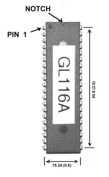
3 Introduction The radio frequency spectrum is filled with noise and other signals, especially those frequencies where unlicensed transmitter operation under FCC part 5 rules is allowed. When using a wireless remote control system it is desirable to have a way of filtering out or ignoring those unwanted signals to prevent false data from activating your control circuits. One way to accomplish this is to use an encoder IC that automatically generates serial coded addresses and data at the transmitter and a decoder IC that deserializes and decodes the addresses and data at the receiver. The addresses generated at the transmitter and decoded at the receiver must match before received data is accepted as valid by the decoder circuit. In the early days of "radio control", before these coding ICs were available, radio controlled garage doors sometimes opened themselves when they received transmissions from a plane passing overhead or a two-way radio operating in the area. Encoding and decoding is now used in most wireless control systems to prevent this type of interference. Glolab GL One chip can be used as either an encoder or decoder Uses only microampere of standby current 409 selectable addresses input / output data ports Operates on 5 volts Uses ceramic resonator for reliable serial data communication Encoder active high data with active high trigger input active low data with active low trigger input Decoder momentary data outputs sequentially latched data outputs outputs source and sink 25 milliamperes The Glolab GL Encoder/Decoder is housed in a 40 pin Plastic Dual Inline Package (PDIP) or a 44 pin Thin Quad Flat Pack (TQFP) package. It is microprocessor based and is designed for use with wireless RF modules, infrared remote controls and other devices that operate with serial input and output data. It may be used as either an encoder or a decoder by simply connecting one pin either high or low. It can encode or decode sixteen bits of data and has twelve address bits for a total of 4,09 addresses. 3
4 ADDRESS ADDRESS 2 2 INPUTS GL ENCODER TMV TRANSMIT MODULE RMV RECEIVE MODULE GL DECODER OUTPUTS 0 0 GROUND GROUND BOLCK DIAGRAM OF TYPICAL TRANSMITTER AND RECEIVER When used as an encoder, one of two Input modes can be selected by connecting a pin either high or low. In one mode the encoding of data can be active high initiated by a high on a transmit enable pin and in another mode the encoding can be active low initiated by a low on a transmit enable pin (the level on this mode pin cannot be changed while the circuits are active or in standby - they must be powered down). When used as a decoder, either momentary or latched data outputs can be selected by connecting a pin either high or low, A momentary valid transmit output indicates when valid data is being received. The GL maintains continuous reception of transmitted data even if some data bits change during transmission. Unlike some decoders that produce a momentary interrupt of all received data when any transmitted data bit changes, the GL will continue to receive unchanged data bits without interruption. For example, if bits and 2 are being transmitted and bit is turned off, bit 2 will continue to be received without interruption. This is an important feature in the remote control of multi-function machinery. The GL is powered by 5 volts and draws about 3.5 milliamperes not including loads when active. When not encoding or decoding it remains in a low power mode where it draws only microampere making it ideal for battery powered applications. As an encoder it becomes active when triggered by transmit enable input. As a decoder it becomes active when it receives serial data. An internal clock is generated by a 4 MHz ceramic resonator which provides more accurate frequency control and therefore better serial data synchronization than the resistor controlled oscillators used in some encoders and decoders. This allows higher speed data transfer without the risk of lost data. Figure shows the pin configuration for the 40 pin PDIP package. The labeled pins serve a common function in both the encoder and decoder. The functions of the remaining pins are described in the following sections. 4
5 ADDRESS 0 ADDRESS ADDRESS 2 ADDRESS 3 ADDRESS 4 ADDRESS 5 ADDRESS PULLDOWN ADDRESS 7 RESONATOR RESONATOR ADDRESS 8 ADDRESS 9 ADDRESS 0 ADDRESS FIGURE 5
6 Addressing There are 2 address pins that can be used to select 4,09 different addresses by connecting them in binary format to either Vss or Vdd. Address pins must be connected the same in an encoder/decoder pair in order for the decoder to receive data from the encoder. Addressing is used to give a unique identity to one pair of encoded devices such as an RF transmitter and receiver and to distinguish that pair from another that has its address pins connected for a different address. This allows a transmission from a transmitter/receiver pair to be received only by its own receiver. Also, by changing addresses, a transmitter can send to a different receiver that matches its new address. All address pins must be connected to either Vdd or Vss by being hard wired, through a DIP or other type of switch or by a logic or other type circuit or through resistors. They cannot be floating. Since it is difficult to find double throw DIP switches that will connect to either Vss or Vdd, pulldown resistors may be connected to the address pins and standard single throw DIP switches can then selectively connect the address pins to Vdd. This would normally result in increased standby current, however, a switched pulldown pin has been provided that goes high during standby to turn pulldown current off. This pin is described below. It should be noted that the use of different addresses does not imply the possibility of full duplex operation or of simultaneous transmission by more than one RF transmitter on the same frequency in close proximity. Switched pulldown Pin 9 is a switched pulldown that goes down to Vss only while the circuit is active and goes high to Vdd during standby. Figure 2 shows how this pin can be used to save power during standby. In this example, DIP switches selectively connect the address pins to Vdd while pulldown resistors pull pins having open switches down to Vss through pin 9 when the circuit is active. Pulldown resistors connected to closed switches use no power when pin 9 is high during standby. This allows the use of standard single throw DIP switches. Pulldown resistors that are returned to pin 9 can also be used with DIP or other single throw switches to set the state of the data-in pins when operating in the active high mode. Pin 9 can sink 25 milliamperes and can also be used to turn a PFET on that can provide Vdd power to peripheral circuits. Resonator A 4 MHz ceramic resonator of the type that has three pins and contains internal capacitors to minimize components is recommended for oscillator frequency control. 4 MHz Resonators are available from Digi-Key and from other distributors. A quartz crystal may also be used, however a 27 pf ceramic capacitor is required from each side of the crystal to ground. Resonator connections are shown in figure 2.
7 ADDRESS SWITCHES 4 MHz RESONATOR FIGURE 2 7
8 Power supply The GL can be powered with 5 volts from a battery or other power source. A 5 volt low dropout micropower voltage regulator such as the Seiko S82C50AY in a TO92 package, available from Mouser Electronics is recommended for operating the encoder or decoder from a 9 volt battery. Encoder Function Figure 3 shows the GL configured an encoder. The encoder function is selected by connecting pin 9 to Vdd. Input modes Two different input modes are selectable by connecting pin 20 to either Vdd or Vss. The Vdd connection causes the transmit enable and all sixteen data in pins to be active high. A low to high level transition on the transmit enable pin will initiate a transmit sequence A high level on a data input pin will produce a high level on the corresponding serial output data bit that drives an RF transmitter module or infrared LED. Transmit enable is also a zero bit. A low to high transition on this pin alone will send zero data. To send a bit other than zero, both transmit enable and the input pin to be sent must go high. For example, to send a, both data in and transmit enable must go high. This can be accomplished by connecting diodes from each data input pin to transmit enable as shown in the applications circuit of figure 7. When pin 20 is connected to Vss the transmit enable and all data in pins become active low. A high to low transition on the transmit enable pin will initiate a transmit sequence and a low level on any data in pin will produce a high level on the corresponding serial data output Bit. The active low function is convenient for use with push button switch inputs when one end of each button is grounded. Transmit enable is transition activated. An enabling transition must occur after power is applied to the GL in order to start a transmission. Transmit enable and data input pins cannot be floating. They are usually driven by logic or other circuits in this mode. When switches are used for inputs, pullup or pulldown resistors can be used with push button or toggle switches to provide a high or low state when the switches are open. 8
9 ADDRESS 0 ADDRESS ADDRESS 2 ADDRESS 3 ADDRESS 4 ADDRESS 5 ADDRESS PULLDOWN ADDRESS 7 RESONATOR RESONATOR ADDRESS 8 ADDRESS 9 ADDRESS 0 ADDRESS INPUT MODE + / SERIAL OUT DATA IN DATA IN 5 DATA IN 4 DATA IN 3 DATA IN 2 DATA IN TRANSMIT ENABLE DATA IN 0 DATA IN 9 DATA IN 8 DATA IN 7 DATA IN DATA IN 5 DATA IN 4 DATA IN 3 DATA IN 2 DATA IN FIGURE 3 9
10 Serial output The serial output generated by the encoder at pin 40 when a transmit sequence is initiated consists of four bytes. The first two bytes contain address bits and the second two contain data bits. Address and data bytes are sent at least three times (one packet) when a transmit sequence is initiated regardless of how short a time transmit is enabled in either active high or active low modes. Transmission of these packets will repeat as long as transmit is enabled. The time required to send a packet is about 30 milliseconds. The transmission rate is 5,000 bits per second. Decoder Function Figure 4 shows the GL- configured as a decoder. The decoder function is selected by connecting pin 9 to Vss. Serial input The address + data packet of serial output generated by the encoder and sent by wireless, infra red or other means are received by an RF receiver module, photo transistor or other receiving device and fed into serial input pin 40 of the decoder. The packet is stored and the groups of address bytes within it are compared with the decoder address pin settings, usually set by DIP switches. The three groups of address and data bytes within the packet are compared with each other and if at least two groups match and if the received address matches the switch settings, the data is passed to the output pins. Output modes Two different output modes are selectable by connecting pin 20 to either Vdd or Vss. When pin 20 is connected to Vdd the valid data pin and all sixteen data outputs become momentary and will produce output only for as long as valid data is being received. When pin 20 is connected to Vss all sixteen data out pins latch their data. In this mode, if a high level appears on an output pin or pins it will remain there even after data is no longer being received. The outputs will not change state until new data is received. Latched outputs are sequential. For example if a high level bit is sent it will latch high. Then if a high level bit 2 is sent, bit will go low and bit 2 will go high. If multiple bits are sent simultaneously, all received bits will latch high. All of the latched bits can be reset to low levels remotely by sending a zero bit. The valid data pin will produce a momentary high level for as long as valid data is being received even if that data is a zero. The valid data pin and the output pins are each capable of both sourcing and sinking 25 milliamperes. 0
11 ADDRESS 0 ADDRESS ADDRESS 2 ADDRESS 3 ADDRESS 4 ADDRESS 5 ADDRESS PULLDOWN ADDRESS 7 RESONATOR RESONATOR ADDRESS 8 ADDRESS 9 ADDRESS 0 ADDRESS MOMENTARY/LATCH SERIAL IN DATA OUT DATA OUT 5 DATA OUT 4 DATA OUT 3 DATA OUT 2 DATA OUT VALID DATA DATA OUT 0 DATA OUT 9 DATA OUT 8 DATA OUT 7 DATA OUT DATA OUT 5 DATA OUT 4 DATA OUT 3 DATA OUT 2 DATA OUT FIGURE 4
12 Basic transmitter Figures 5 shows a basic implementation of the GL as it is used with an RF transmit module. The input mode is usually defined by the application and pin 20 can be hard wired to either Vss for active low input mode or Vdd for active high input mode. It is shown wired to Vdd for active high mode. Address selection will not be necessary for many applications especially where only one RF transmitter pair will be used or for infrared remote control applications. For these applications the address pins that are shown hard wired to Vss can be wired to either Vss or Vdd. Where address selection is necessary, pulldown resistors to pin 9 can be used together with standard DIP switches that selectively connect address pins to Vdd. GL- DATA 2 20 ANTENNA DATA DATA DATA 4 DATA 5 DATA DATA 7 DATA CR C2. TMV TRANSMIT MODULE DATA DATA 0 C TRANSMIT ENABLE PD DATA 34 7 DATA 2 35 DATA DATA 4 DATA 5 DATA REG D + 9V 2
13 FIGURE 5 Basic receiver Figures shows a basic implementation of the GL as it is used with an RF receive module. The selection of latched or momentary mode controlled by pin 20 is usually defined by the application so pin 20 can be hard wired to either Vss or directly or through a resistor to Vdd. Figure shows it wired to Vdd for momentary mode. Address pins can be connected to Vss or Vdd. They are all wired to Vss to match the transmitter connections of figure 5. Each data output can source or sink 25 milliamperes but the total simultaneous currents must not exceed 200 milliamperes. ANTENNA RMV RECEIVE MODULE SERIAL DATA GL DATA OUT 3 38 DATA OUT DATA OUT DATA OUT 3 35 DATA OUT DATA OUT 8 33 PD 9 32 C DATA OUT DATA OUT 9 CR DATA OUT 8 DATA OUT DATA OUT 25 DATA OUT 5 + N400 REG 5 VDC DATA OUT 4 DATA OUT 3 DATA OUT VDC _ DATA OUT VALID DATA GROUND FIGURE 3
14 GL versions GLPDIP Gl in a 40 pin Plastic Dual Inline Package (PDIP) for through hole or socket mounting. GLTQFP Gl in a 44 pin surface mount Thin Quad Flat Pack (TQFP). GL IN TQFP PACKAGE DIP TO TQFP PIN TRANSLATION TABLE TQFP PINS 2, 3, 33, 34 NOT USED, NO CONNECTION (NC) DIP PIN TQFP PIN DIP PIN TQFP PIN DIP PIN TQFP PIN DIP PIN TQFP PIN
15 Specifications Absolute maximum ratings Ambient temperature under power to + 25 Storage temperature to +50 Voltage on any pin (except Vdd) with respect to Vss to Vdd + 0.V Voltage on Vdd with respect to Vss to +7.5V Input clamp current ±20 ma Output clamp current ±20 ma Maximum current sunk by an output pin ma Maximum current sourced by an output pin ma Standard operating conditions PARAMETER MIN TYP MAX UNITS Operating temperature C Supply voltage (Vdd) V Supply current () 3.5 ma Power down standby current µa Reset voltage (2) V Pin 9 pulldown current 25 ma Input leakage current ±.0 µa Input high voltage 2.0 Vdd V Input low voltage Vss 0.8 V Output high voltage (3) Vdd -0.7 V Output low voltage (4) 0. V Output source current 25 ma Output sink current 25 ma Transmit enable pulse width 00 ns Transmit time - packet 30 ms () Not including output loads or pullup resistors. (2) Supplied by VDR device. (3) Output current = 3 ma, Vdd = 4.5V (4) Output current = 8.5 ma, Vdd = 4.5V 5
16 Applications Although Glolab is not a parts distributor we stock some of the parts used in the applications circuits that are also available from distributors so project builders can collect the necessary parts without having to buy from many distributors and pay multiple minimum quantity and shipping costs. Glolab Parts list The following are parts used in the applications circuits that are available from Glolab. DESCRIPTION PART NUMBER SOURCE Transmitter module TMV Glolab Receiver module RMV Glolab Encoder/Decoder GLPDIP Glolab Encoder/Decoder GLTQFP Glolab 4 MHz ceramic resonator CR4 Glolab Distributor Parts list The following are parts used in the applications circuits that are available from electronics parts distributors. DESCRIPTION MFG PART NUMBER SOURCE PART NUMBER 4 MHz ceramic resonator ECS ZTT-4.00MG ECS ZTT-4.00MG Panasonic EFOMC4004A4 Digi-Key X902 Mouser 520-ZTT400MG Digi-Key PX400 Voltage regulator LDO 5V Seiko 82C50AY Mouser 28-82C50AY Digi-Key Mouser
17 Active high push button transmitter Figures 7 is a complete push button transmitter that operates in the input active high mode. The circuit operates from a 9 volt battery and uses only 3 microamperes of current when no buttons are being pressed. All address pins can be set by a 2 position DIP switch giving 4,09 possible addresses. Pressing button 0 will activate the valid data pin in a receiver. Pressing - will activate valid data and one or more data out pins in a receiver. Multiple buttons may be pressed to send up to bits simultaneously. Latched receiver outputs can be reset by pressing button 0 TRANSMIT ENABLE PB0 D2 - D7 N94 PB PB2 PB3 GL ADDRESSS SWITCHES R8 - R29 00K ANTENNA PB4 PB5 PB PB7 PB CR4 TMV TRANSMIT MODULE PB C2. PB IC PB 34 7 PB2 35 PB3 3 5 PB4 PB5 PB Vdd Vss R - R7 00K Vss + +5 Vdd C 00 IC3 IN94 D + 9V FIGURE 7 7
18 Momentary output receiver Figures 8 is a complete receiver circuit having momentary outputs. The decoder drives open collector bipolar transistors in TO92 packages that can sink 200 milliamperes to power relays or other loads directly. The momentary function can be used for wireless control of machinery or any device that has to be energized while a remote control button is being pressed. The Valid Data LED will be on whenever any other data pin is on. The data outputs may be energized either individually or simultaneously. Outputs may be operated in the latched mode by connecting pin 20 to Vss. Latched outputs can be reset from the transmitter by sending a zero bit. The twelve address switches should be set the same as in the transmitter encoder. Power may be supplied by a 2 volt wall transformer and regulated down to 5 volts by a 7805 regulator IC3. ANTENNA RMV RECEIVE R4- R30 K 2N440 OUTPUT OUTPUT 5 MODULE OUTPUT 4 GL OUTPUT OUTPUT OUTPUT OUTPUT OUTPUT 9 C IC OUTPUT 8 OUTPUT 7 ADDRESS SWITCHES CR OUTPUT OUTPUT 5 + N400 R - R2 00K IC3 5 VDC 9-5 D + C + C2 VDC _ OUTPUT 4 OUTPUT 3 OUTPUT 2 OUTPUT VALID DATA GROUND FIGURE 8 8

19 9
20 GLOLAB CORPORATION 307 Pine Ridge Drive Wappingers Falls, NY 2590 (845) Fax - (845) lab@glolab.com Glolab Corp. 20
GL-104 ENCODER/DECODER MANUAL GLOLAB CORPORATION
 GL-04 ENCODER/DECODER MANUAL GLOLAB CORPORATION Thank you for buying our Encoder / Decoder Module. The goal of Glolab is to produce top quality electronic kits, products and components. All of our kits
+Denotes a lead(pb)-free/rohs-compliant package.
-free/rohs-compliant package.") EVALUATION KIT AVAILABLE MAX7320 General Description The MAX7320 2-wire serial-interfaced peripheral features eight push-pull outputs with selectable power-up logic states. The +5.5V tolerant RST input
EVALUATION KIT AVAILABLE MAX7320 General Description The MAX7320 2-wire serial-interfaced peripheral features eight push-pull outputs with selectable power-up logic states. The +5.5V tolerant RST input
Fremont Micro Devices, Inc.
 FEATURES Low voltage and low power operations: FT24C02/04/08/16: V CC = 2.5V to 5.5V FT24C02A/04A/08A/16A: V CC = 1.8V to 5.5V Maximum Standby current < 1µA (typically 0.02µA and 0.06µA @ 1.8V and 5.5V
MIC1832. General Description. Features. Applications. Typical Application
 3.3V Voltage Supervisor with Manual Reset, Watchdog Timer and Dual Reset Outputs General Description The is a low-current microprocessor supervisor for monitoring 3.3V and 3V systems. The device features
DS1306. Serial Alarm Real Time Clock (RTC)
") www.dalsemi.com FEATURES Real time clock counts seconds, minutes, hours, date of the month, month, day of the week, and year with leap year compensation valid up to 2100 96-byte nonvolatile RAM for data
www.dalsemi.com FEATURES Real time clock counts seconds, minutes, hours, date of the month, month, day of the week, and year with leap year compensation valid up to 2100 96-byte nonvolatile RAM for data
Features. Ordering Information. Selector Guide. Applications. Pin Configurations. I 2 C Port Expander with 8 Open-Drain I/Os
 General Description The MAX7321 2-wire serial-interfaced peripheral features eight open-drain I/O ports with selectable internal pullups and transition detection. Any port may be used as a logic input
Remote Control Decoder IC
 DESCRIPTION is a remote control decoder paired with PT2260 or PT2262 utilizing CMOS Technology. It has 12-bit of tri-state address pins providing a maximum of 531,441 (or 3 12 ) address codes; thereby
HT6P Learning Decoder
 2 24 Learning Decoder Features Operating voltage: 2.4V~5.2V Low power and high noise immunity CMOS technology Capable of decoding 24-bit information Pair with HOLTEK s 2 24 programmable encoders (HT6P20)
MHz TRANSCEIVER. Bi-Directional Send and Receive. Compatible with: Transmitter Receiver Transceiver. Part # Part #
 433.92 MHz TRANSMITTER 433.92 MHz TRANSCEIVER 433.92 MHz RECEIVER Part # 27986 Part # 27988 Part # 27987 Single Direction Send Only Bi-Directional Send and Receive Single Direction Receive Only Compatible
DS1845 Dual NV Potentiometer and Memory
 www.maxim-ic.com FEATURES Two linear taper potentiometers -010 one 10k, 100 position & one 10k, 256 position -050 one 10k, 100 position & one 50k, 256 postition -100 one 10k, 100 position & one 100k, 256
V PP IN V CC3 IN V CC5 IN EN0 EN1 MIC2561 V CC5_EN V CC3_EN
 MIC2561 PCMCIA Card Socket and V PP Switching Matrix Final Information General Description The MIC2561 & V PP Matrix controls PCMCIA (Personal Computer Memory Card International Association) memory card
and 8 Open-Drain I/Os
 EVALUATION KIT AVAILABLE MAX7325 General Description The MAX7325 2-wire serial-interfaced peripheral features 16 I/O ports. Ports are divided into eight push-pull outputs and eight I/Os with selectable
24C08/24C16. Two-Wire Serial EEPROM. Preliminary datasheet 8K (1024 X 8)/16K (2048 X 8) General Description. Pin Configuration
/16K (2048 X 8) General Description. Pin Configuration") Two-Wire Serial EEPROM Preliminary datasheet 8K (1024 X 8)/16K (2048 X 8) Low-voltage Operation 1.8 (VCC = 1.8V to 5.5V) Operating Ambient Temperature: -40 C to +85 C Internally Organized 1024 X 8 (8K),
Two-Wire Serial EEPROM Preliminary datasheet 8K (1024 X 8)/16K (2048 X 8) Low-voltage Operation 1.8 (VCC = 1.8V to 5.5V) Operating Ambient Temperature: -40 C to +85 C Internally Organized 1024 X 8 (8K),
12 Push-Pull Outputs and 4 Inputs
 EVALUATION KIT AVAILABLE MAX7326 General Description The MAX7326 2-wire serial-interfaced peripheral features 16 I/O ports. The ports are divided into 12 push-pull outputs and four input ports with selectable
UNISONIC TECHNOLOGIES CO.,LTD. UL318 Preliminary LINEAR INTEGRATED CIRCUIT
 UNISONIC TECHNOLOGIES CO.,LTD. UL318 Preliminary LINEAR INTEGRATED CIRCUIT SERIAL-INTERFACED 10-DIGIT LED CONTROLLER IC WITH KEYSCAN DESCRIPTION The UL318 is a compact LED controller and driver that interface
4-Megabit (512K x 8) 5-volt Only CMOS Flash Memory AT49F040 AT49F040T AT49F040/040T AT49F040/040T. Features. Description. Pin Configurations
 5-volt Only CMOS Flash Memory AT49F040 AT49F040T AT49F040/040T AT49F040/040T. Features. Description. Pin Configurations") Features Single Voltage Operation 5V Read 5V Reprogramming Fast Read Access Time - 70 ns Internal Program Control and Timer 16K bytes Boot Block With Lockout Fast Erase Cycle Time - 10 seconds Byte By
Features Single Voltage Operation 5V Read 5V Reprogramming Fast Read Access Time - 70 ns Internal Program Control and Timer 16K bytes Boot Block With Lockout Fast Erase Cycle Time - 10 seconds Byte By
PCR43304R, PCR43304RE 4-Channel, 433MHz Penta Receiver with Frequency Hopping
 PCR43304R, PCR43304RE 4-Channel, 433MHz Penta Receiver with Frequency Hopping Features Frequency hopping between 433.10 to 434.70MHz 12-way dipswitch or encrypted coding Momentary and latching modes are
OSC Ring Type Ring or Resonator type (optional) RESET Pin No Yes
 RESET Pin No Yes") General Description Features est Series is a series of 3 to 340 seconds single chip high quality voice synthesizer IC which contains one 4-bit Input port (provided for est005 and above); three 4-bit I/O
General Description Features est Series is a series of 3 to 340 seconds single chip high quality voice synthesizer IC which contains one 4-bit Input port (provided for est005 and above); three 4-bit I/O
AT45DQ321. Features. 32-Mbit DataFlash (with Extra 1-Mbits), 2.3V Minimum SPI Serial Flash Memory with Dual-I/O and Quad-I/O Support
, 2.3V Minimum SPI Serial Flash Memory with Dual-I/O and Quad-I/O Support") 32-Mbit DataFlash (with Extra 1-Mbits), 2.3V Minimum SPI Serial Flash Memory with Dual-I/O and Quad-I/O Support Features Single 2.3V - 3.6V supply Serial Peripheral Interface (SPI) compatible Supports
32-Mbit DataFlash (with Extra 1-Mbits), 2.3V Minimum SPI Serial Flash Memory with Dual-I/O and Quad-I/O Support Features Single 2.3V - 3.6V supply Serial Peripheral Interface (SPI) compatible Supports
ACE24AC02A1 Two-wire Serial EEPROM
 Description The ACE24AC02A1 is 2048 bits of serial Electrical Erasable and Programmable Read Only Memory, commonly known as EEPROM. They are organized as 256 words of 8 bits (1 byte) each. The devices
E3B USER'S GUIDE. for QT310 / QT320 QProx IC evaluation and development Overview. Fast Start
 E3B USER'S GUIDE for QT310 / QT320 QProx IC evaluation and development Overview The E3B board works with Quantum s QT310 and QT320 QProx ICs. Either device can be inserted into the 8-pin DIP socket. QT310
DS1676 Total Elapsed Time Recorder, Erasable
 www.dalsemi.com Preliminary DS1676 Total Elapsed Time Recorder, Erasable FEATURES Records the total time that the Event Input has been active and the number of events that have occurred. Volatile Elapsed
Preliminary Data MOS IC. Type Ordering Code Package SDA Q67100-H5092 P-DIP-8-1
 Nonvolatile Memory 1-Kbit E 2 PROM SDA 2516-5 Preliminary Data MOS IC Features Word-organized reprogrammable nonvolatile memory in n-channel floating-gate technology (E 2 PROM) 128 8-bit organization Supply
Home Security System with Remote Home Automation Control
 Home Security System with Remote Home Automation Control Justin Klumpp Senior Project Hardware Description Western Washington University April 24 2005 Professor Todd Morton Introduction: This document
ES-562/564U COMBINATION CLOCK/TIMER
 142 SIERRA ST., EL SEGUNDO, CA 90245 USA (310)322-2136 FAX (310)322-8127 www.ese-web.com ES-562/564U COMBINATION CLOCK/TIMER OPERATION AND MAINTENANCE MANUAL The ES-562U/564U is a combination six digit
MIC705/706/707/708. General Description. Features. Applications. Typical Application. µp Supervisory Circuit
 µp Supervisory Circuit General Description The MIC705, MIC706, MIC707, and MIC708 are inexpensive microprocessor supervisory circuits that monitor power supplies in microprocessor-based systems. The circuit
3. The MC6802 MICROPROCESSOR
 3. The MC6802 MICROPROCESSOR This chapter provides hardware detail on the Motorola MC6802 microprocessor to enable the reader to use of this microprocessor. It is important to learn the operation and interfacing
Features VCC MIC1810 RESET RESET
 Microprocessor Reset Circuit General Description The is an inexpensive microprocessor supervisory circuit that monitors power supplies in microprocessor based systems. The function of these devices is
ACE24AC16B Two-wire Serial EEPROM
 Description The ACE24AC16B is 16,384 bits of serial Electrical Erasable and Programmable Read Only Memory, commonly known as EEPROM. They are organized as 2,048 words of 8 bits (1 byte) each. The devices
PCR43301RE 1-Channel, 433MHz Penta Receiver with Frequency Hopping
 PCR43301RE 1-Channel, 433MHz Penta Receiver with Frequency Hopping Features Frequency hopping between 433.10 to 434.70MHz 12-way dipswitch or encrypted coding Compatible with PentaFOB and PentaCODE remotes
Low-Power-Radio Transceiver IC
 Addressed Mode With Acknowledge Broadcast Mode Automatic Retry Serial Interface Stand Alone Operation Achieves Maximum Range From RF Modules Flow Control Option Two Telemetry I/O Lines (addressed mode
FM24CL04 4Kb FRAM Serial Memory
 4Kb FRAM Serial Memory Features 4K bit Ferroelectric Nonvolatile RAM Organized as 512 x 8 bits Unlimited Read/Writes 45 Year Data Retention NoDelay Writes Advanced High-Reliability Ferroelectric Process
ACE24AC02A3C Two-wire Serial EEPROM
 Description The ACE24AC02A3C is 2048 bits of serial Electrical Erasable and Programmable Read Only Memory, commonly known as EEPROM. They are organized as 256 words of 8 bits (1 byte) each. The devices
Preliminary Data MOS IC. Type Ordering Code Package SDA Q67100-H5096 P-DIP-8-1
 Nonvolatile Memory 4-Kbit E 2 PROM with I 2 C Bus Interface SDA 2546-5 Preliminary Data MOS IC Features Word-organized reprogrammable nonvolatile memory in n-channel floating-gate technology (E 2 PROM)
.200 Ht 60 lead, flat-pack, W x 1.59 L x.147 Ht OPERATIONAL ENVIRONMENT Temperature Range: -55 C to +125 C
 MIL-STD-1553 CT1820 Data Terminal Bit Processor For MIL-STD 1553 A&B Released Datasheet September 30 th, 2016 The most important thing we build is trust FEATURES Operates from +5VDC @ 50mA 300mW typical
AS Channels Capacitive Touch Sensor IC From Santa Clara, United States of America
 ASI Competitor Equivalent A Competitor Equivalent B Volts Leading Performance: ESD HBM >8k Volts (Directly Applied to All IC Pins) Operating Temperature up to >+95 0 C Features Overview Analog and Digital
Lost Item Pager. Project Description. Russ Kinley
 Lost Item Pager Project Description Russ Kinley Introduction The lost item pager will have a base unit that is stationary, consisting of a few page buttons and a digital display. Each of the buttons will
PCR43304R, PCR43304RE 4-Channel, 433MHz Penta Receiver with Frequency Hopping
 PCR43304R, PCR43304RE 4-Channel, 433MHz Penta Receiver with Frequency Hopping Features Frequency hopping between 433.10 to 434.70MHz 12-way dipswitch or encrypted coding Momentary and latching modes are
ES-362U PRESETTABLE MASTER TIMER
 142 SIERRA ST., EL SEGUNDO, CA 90245 USA (310)322-2136 FAX (310)322-8127 www.ese-web.com ES-362U PRESETTABLE MASTER TIMER OPERATION AND MAINTENANCE MANUAL The ES-362U is a four digit, presettable 100 minute
HCTL-2017 Quadrature Decoder/Counter Interface ICs
 Products > Motion Control Encoder Solutions > Integrated Circuits > Decoder > HCTL-2017 HCTL-2017 Quadrature Decoder/Counter Interface ICs Description HCTL-2xxx series is a direct drop-in replacement for
ACE24AC128 Two-wire Serial EEPROM
 Description The ACE24AC128 series are 131,072 bits of serial Electrical Erasable and Programmable Read Only Memory, commonly known as EEPROM. They are organized as 16,384 words of 8 bits (one byte) each.
DS1302. Trickle Charge Timekeeping Chip FEATURES PIN ASSIGNMENT PIN DESCRIPTION
 DS132 Trickle Charge Timekeeping Chip FEATURES Real time clock counts seconds, minutes, hours, date of the month, month, day of the week, and year with leap year compensation valid up to 21 31 x 8 RAM
Table 1 Brief Specifications
 Rev.1.1 MICROCOMPUTER WITH BUILT-IN PAGING DECODER The microcomputer incorporates a decoder conforming to CCIR Radio Paging Decode 1(POCSA Code), a melody generator, an LCD driver and a timer. Only attaching
PAK-XI PS/2 Coprocessor Data Sheet by AWC
 PAK-XI PS/2 Coprocessor Data Sheet 1999-2003 by AWC AWC 310 Ivy Glen League City, TX 77573 (281) 334-4341 http://www.al-williams.com/awce.htm V1.0 30 Oct 2003 Table of Contents Overview...1 If You Need
AT24C01A/02/04/08/16. 2-Wire Serial CMOS E 2 PROM. Features. Description. Pin Configurations. 1K (128 x 8) 2K (256 x 8) 4K (512 x 8) 8K (1024 x 8)
 2K (256 x 8) 4K (512 x 8) 8K (1024 x 8)") AT24C01A/02/04/08/16 Features Low Voltage and Standard Voltage Operation 5.0 (V CC = 4.5V to 5.5V) 2.7 (V CC = 2.7V to 5.5V) 2.5 (V CC = 2.5V to 5.5V) 1.8 (V CC = 1.8V to 5.5V) Internally Organized 128
AT24C01A/02/04/08/16 Features Low Voltage and Standard Voltage Operation 5.0 (V CC = 4.5V to 5.5V) 2.7 (V CC = 2.7V to 5.5V) 2.5 (V CC = 2.5V to 5.5V) 1.8 (V CC = 1.8V to 5.5V) Internally Organized 128
DS1305 Serial Alarm Real Time Clock (RTC)
") Serial Alarm Real Time Clock (RTC) www.dalsemi.com FEATURES Real time clock counts seconds, minutes, hours, date of the month, month, day of the week, and year with leap year compensation valid up to 2100
Serial Alarm Real Time Clock (RTC) www.dalsemi.com FEATURES Real time clock counts seconds, minutes, hours, date of the month, month, day of the week, and year with leap year compensation valid up to 2100
Low Voltage, 10-Bit Digital Temperature Sensor in 8-Lead MSOP AD7314
 a FEATURES 10-Bit Temperature-to-Digital Converter 35 C to +85 C Operating Temperature Range 2 C Accuracy SPI and DSP Compatible Serial Interface Shutdown Mode Space-Saving MSOP Package APPLICATIONS Hard
Drawing code Package Tape Reel 8-Pin DIP DP008-F 8-Pin SOP(JEDEC) FJ008-A FJ008-D FJ008-D 8-Pin TSSOP FT008-A FT008-E FT008-E
 FJ008-A FJ008-D FJ008-D 8-Pin TSSOP FT008-A FT008-E FT008-E") Rev. 3.2_ CMOS SERIAL E 2 PROM Features The is a high speed, low current consumption, 8 K-bit serial E 2 PROM with a wide operating voltage range. It is organized as 512-word 16-bit respectively. Each
Rev. 3.2_ CMOS SERIAL E 2 PROM Features The is a high speed, low current consumption, 8 K-bit serial E 2 PROM with a wide operating voltage range. It is organized as 512-word 16-bit respectively. Each
M68HC705L4 PROGRAMMER BOARD APPLICATION NOTE
 M68HC705L4PGMR JUNE 1992 M68HC705L4 PROGRAMMER BOARD (REVision A PWBs only) APPLICATION NOTE INTRODUCTION This application note describes the programming technique used to program and verify the XC68HC705L4
512K bitstwo-wire Serial EEPROM
 General Description The provides 524,288 bits of serial electrically erasable and programmable read-only memory (EEPROM), organized as 65,536 words of 8 bits each. The device is optimized for use in many
Features. Applications
 Micro-Power Voltage Supervisor IttyBitty General Description The is a power supply supervisor that provides undervoltage monitoring, manual reset capability, and power-on reset generation in a compact
DS 1682 Total Elapsed Time Recorder with Alarm
 DS 1682 Total Elapsed Time Recorder with Alarm www.dalsemi.com FEATURES Records the total time that the Event Input has been active and the number of events that have occurred. Volatile Elapsed Time Counter
Shack Clock kit. U3S Rev 2 PCB 1. Introduction
 Shack Clock kit U3S Rev 2 PCB 1. Introduction Thank you for purchasing the QRP Labs Shack Clock kit. This clock uses the Ultimate3S QRSS/WSPR kit hardware, but a different firmware version. It can be used
ELSEMA GLR Applications Automatic gates. Security systems. Timer controlled outputs. Simple on/off functions.
 GLR43301 Single Channel 433MHz Gigalink Receiver with Timer Controlled Relay Output Features Wide supply connection 10.0 to 28.0 Volts AC/DC Highly sensitive receiver input stage. When used with GLT433
1-Megabit (128K x 8) 5-volt Only Flash Memory AT29C010A. Features. Description. Pin Configurations
 5-volt Only Flash Memory AT29C010A. Features. Description. Pin Configurations") Features Fast Read Access Time - 70 ns 5-Volt Only Reprogramming Sector Program Operation Single Cycle Reprogram (Erase and Program) 1024 Sectors (128 bytes/sector) Internal Address and Data Latches for
Features Fast Read Access Time - 70 ns 5-Volt Only Reprogramming Sector Program Operation Single Cycle Reprogram (Erase and Program) 1024 Sectors (128 bytes/sector) Internal Address and Data Latches for
CMOS SyncFIFO 64 X 9, 256 x 9, 512 x 9, 1,024 X 9, 2,048 X 9, 4,096 x 9 and 8,192 x 9
 Integrated Device Technology, Inc. CMOS SyncFIFO 64 X 9, 256 x 9, 512 x 9, 1,24 X 9, 2,48 X 9, 4,96 x 9 and 8,192 x 9 IDT72421 IDT7221 IDT72211 IDT72221 IDT72231 IDT72241 IDT72251 FEATURES: 64 x 9-bit
DS WIRE INTERFACE 11 DECOUPLING CAP GND
 Rev ; 4/3 Hex Nonvolatile Potentiometer with General Description The contains six 256-position nonvolatile (NV) potentiometers, 64 bytes of NV user EEPROM memory, and four programmable NV I/O pins. The
DS1305EN. Serial Alarm Real-Time Clock
 Serial Alarm Real-Time Clock www.maxim-ic.com FEATURES Real-time clock (RTC) counts seconds, minutes, hours, date of the month, month, day of the week, and year with leap-year compensation valid up to
USB1. Encoder Data Acquisition USB Device Page 1 of 6. Description. Features
 Description USB1 Page 1 of 6 The USB1 is no longer available for purchase, and has been replaced by our recently released USB4. The USB4 is a redesigned, enhanced version of the USB1, and is already available
I 2 C Port Expander with Eight Inputs. Features
 EVALUATION KIT AVAILABLE MAX7319 General Description The MAX7319 2-wire serial-interfaced peripheral fea-tures eight input ports with selectable internal pullups, overvoltage protection to +6V, and transition
PK2200 Series. Features. C-Programmable Controller. Specifications Board Size Enclosure Size Operating Temp.
 C-Programmable Controller P00 Series The P00 Series of C-programmable controllers is based on the Zilog Z80 microprocessor. The P00 includes digital, serial, and high-current switching interfaces. The
PCR43301RE ELSEMA. . and anywhere else you need a wireless signal to transmit a contact closure. Description
 PCR43301RE 1-Channel, 433MHz Penta Receiver with Frequency Hopping Features Frequency hopping between 433.10 to 434.70MHz 12-way dipswitch or encrypted coding Compatible with PentaFOB and PentaCODE remotes
DS1216B. SmartWatch/RAM 16K/64K FEATURES PIN ASSIGNMENT PIN DESCRIPTION
 DS1216B SmartWatch/RAM 16K/64K FEATURES Keeps track of hundredths of seconds, seconds, minutes, hours, days, date of the month, months, and years Converts standard 2K x 8 and 8K x 8 CMOS static RAMs into
MIC826. General Description. Features. Applications. Typical Application
 Voltage Supervisor with Watchdog Timer, Manual Reset, and Dual Outputs In 1.6mm x 1.6mm TDFN General Description The is a low-current, ultra-small, voltage supervisor with manual reset input, watchdog
Am27C Kilobit (8 K x 8-Bit) CMOS EPROM DISTINCTIVE CHARACTERISTICS GENERAL DESCRIPTION BLOCK DIAGRAM V CC V SS V PP
 CMOS EPROM DISTINCTIVE CHARACTERISTICS GENERAL DESCRIPTION BLOCK DIAGRAM V CC V SS V PP") FINAL Am27C64 64 Kilobit (8 K x 8-Bit) CMOS EPROM DISTINCTIVE CHARACTERISTICS Fast access time Speed options as fast as 45 ns Low power consumption 20 µa typical CMOS standby current JEDEC-approved pinout
FINAL Am27C64 64 Kilobit (8 K x 8-Bit) CMOS EPROM DISTINCTIVE CHARACTERISTICS Fast access time Speed options as fast as 45 ns Low power consumption 20 µa typical CMOS standby current JEDEC-approved pinout
DS2223/DS2224. EconoRAM FEATURES PACKAGE OUTLINE. PIN CONNECTIONS Pin 1 GND Ground Pin 2 DQ Data In/Out Pin 3 V CC Supply Pin 4 GND Ground
 DS2223/DS2224 EconoRAM FEATURES Low cost, general purpose, 256 bit memory DS2223 has 256 bit SRAM DS2224 has 32 bit ROM, 224 bit SRAM Reduces control, address and data interface to a single pin PACKAGE
Am27C Megabit (131,072 x 8-Bit) CMOS EPROM DISTINCTIVE CHARACTERISTICS GENERAL DESCRIPTION BLOCK DIAGRAM
 CMOS EPROM DISTINCTIVE CHARACTERISTICS GENERAL DESCRIPTION BLOCK DIAGRAM") FINAL 1 Megabit (131,072 x 8-Bit) CMOS EPROM DISTINCTIVE CHARACTERISTICS Fast access time 45 ns maximum access time Low power consumption 20 µa typical CMOS standby current JEDEC-approved pinout Single
FINAL 1 Megabit (131,072 x 8-Bit) CMOS EPROM DISTINCTIVE CHARACTERISTICS Fast access time 45 ns maximum access time Low power consumption 20 µa typical CMOS standby current JEDEC-approved pinout Single
Am27C128. Advanced Micro Devices. 128 Kilobit (16,384 x 8-Bit) CMOS EPROM DISTINCTIVE CHARACTERISTICS GENERAL DESCRIPTION BLOCK DIAGRAM FINAL
 CMOS EPROM DISTINCTIVE CHARACTERISTICS GENERAL DESCRIPTION BLOCK DIAGRAM FINAL") FINAL 128 Kilobit (16,384 x 8-Bit) CMOS EPROM Advanced Micro Devices DISTINCTIVE CHARACTERISTICS Fast access time 45 ns Low power consumption 20 µa typical CMOS standby current JEDEC-approved pinout Single
FINAL 128 Kilobit (16,384 x 8-Bit) CMOS EPROM Advanced Micro Devices DISTINCTIVE CHARACTERISTICS Fast access time 45 ns Low power consumption 20 µa typical CMOS standby current JEDEC-approved pinout Single
ILI2303. ILI2303 Capacitive Touch Sensor Controller. Specification
 Capacitive Touch Sensor Controller Specification Version: V1.03 Date: 2014/9/17 ILI TECHNOLOGY CORP. 8F, No.38, Taiyuan St., Jhubei City, Hsinchu County 302, Taiwan, R.O.C. Tel.886-3-5600099; Fax.886-3-5600055
DS1305. Serial Alarm Real Time Clock (RTC) FEATURES PIN ASSIGNMENT ORDERING INFORMATION
 FEATURES PIN ASSIGNMENT ORDERING INFORMATION") DS135 Serial Alarm Real Time Clock (RTC) FEATURES Real time clock counts seconds, minutes, hours, date of the month, month, day of the week, and year with leap year compensation valid up to 21 96 byte
DS135 Serial Alarm Real Time Clock (RTC) FEATURES Real time clock counts seconds, minutes, hours, date of the month, month, day of the week, and year with leap year compensation valid up to 21 96 byte
Pm39F010 / Pm39F020 / Pm39F040
 1 Mbit / 2 Mbit / 4 Mbit 5 Volt-only CMOS Flash Memory FEATURES Single Power Supply Operation - Low voltage range: 4.5 V - 5.5 V Memory Organization - Pm39F010: 128K x 8 (1 Mbit) - Pm39F020: 256K x 8 (2
VCC NC PROTECT DI DO. Table 1
 Rev.1.11 CMOS SERIAL E 2 PROM Features Low power consumption Standby :0.8 µa Max. (V CC =5.5 V) Operating :0.8 ma Max. (V CC =5.5 V) 0.4 ma Max. (V CC =2.7 V) Low operating voltage range Write : 1.8 to
DS2405. Addressable Switch PIN ASSIGNMENT
 www.maxim-ic.com FEATURES Open-drain PIO pin is controlled by matching 64-bit, laser-engraved registration number associated with each device Logic level of open drain output can be determined over 1-Wire
USB-4303 Specifications
 Specifications Document Revision 1.0, February, 2010 Copyright 2010, Measurement Computing Corporation Typical for 25 C unless otherwise specified. Specifications in italic text are guaranteed by design.
Product Specification
 Product Specification Features Amp ed RF, Inc. Description 15mm x 27mm The added class 1 power, +18dBm, of the BT-11, gives this module one of the best ranges in the industry. It s completely pin compatible
INTEGRATED CIRCUITS. PCA bit I 2 C and SMBus I/0 port with reset. Product data Supersedes data of 2002 May Dec 13
 INTEGRATED CIRCUITS Supersedes data of 2002 May 13 2002 Dec 13 Philips Semiconductors FEATURES Lower voltage, higher performance migration path for the PCA9556 8 general purpose input/output expander/collector
Sierra Radio Systems. Making a Keyer with the. HamStack. Project Platform
 Sierra Radio Systems Making a Keyer with the HamStack Project Platform Introduction The HamStack Project Board includes primary interface elements needed to make a high quality CW keyer. Using the LCD
Remote 16-bit I/O expander for Fm+ I 2 C-bus with interrupt and reset. Description
 Remote 16-bit I/O expander for Fm+ I 2 C-bus with interrupt and reset Features Operation power supply voltage from 2.3V to 5.5V 16-bit remote I/O pins that default to inputs at powerup 1 MHz I 2 C-bus
commodore semiconductor group NMOS 950 Rittenhouse Rd., Norristown, PA Tel.: 215/ TWX: 510/ (MEMORY, I/O, TIMER ARRAY)
") commodore semiconductor group NMOS 950 Rittenhouse Rd., Norristown, PA 19403 Tel.: 215/666-7950 TWX: 510/660-4168 6532 (MEMORY, I/O, TIMER ARRAY) THE 6532 CONCEPT- The 6532 is designed to operate in conjunction
commodore semiconductor group NMOS 950 Rittenhouse Rd., Norristown, PA 19403 Tel.: 215/666-7950 TWX: 510/660-4168 6532 (MEMORY, I/O, TIMER ARRAY) THE 6532 CONCEPT- The 6532 is designed to operate in conjunction
Suprex RF Series CYPRESS. Operations Manual. Suprex Reader Extender - RF Wireless Interface EXP SPX Mhz SPX-5521_MAN_0316
 CYPRESS Suprex RF Series Operations Manual Suprex Reader Extender - RF Wireless Interface EXP-2000 SPX-5521 900 Mhz SPX-5521_MAN_0316 Cypress Suprex SPX-5521 Series Overview This manual covers the operation
ACE24AC64 Two-wire Serial EEPROM
 Description The ACE24AC64 series are 65,536 bits of serial Electrical Erasable and Programmable Read Only Memory, commonly known as EEPROM. They are organized as 8192 words of 8 bits (one byte) each. The
DS1238A MicroManager PIN ASSIGNMENT PIN DESCRIPTION V BAT V CCO V CC
 MicroManager www.dalsemi.com FEATURES Holds microprocessor in check during power transients Halts and restarts an out-of-control microprocessor Warns microprocessor of an impending power failure Converts
STM706T/S/R, STM706P, STM708T/S/R
 STM706T/S/R, STM706P, STM708T/S/R 3 V supervisor Features Datasheet - production data Precision monitor T: 3.00 V V RST 3.15 V S: 2.88 V V RST 3.00 V R: STM706P: 2.59 V V RST 2.70 V RST and RST outputs
A24C08. AiT Semiconductor Inc. ORDERING INFORMATION
 DESCRIPTION The provides 8192 bits of serial electrically erasable and programmable read-only memory (EEPROM), organized as 1024 words of 8 bits each. The device is optimized for use in many industrial
Debounced 8 8 Key-Scan Controller
 Debounced 8 8 Key-Scan Controller Description The SN7326 is a 64 key, key-scan controller. It offloads the burden of keyboard scanning from the host processor. The SN7326 supports keypad matrix of up to
Am27C Megabit (128 K x 16-Bit) CMOS EPROM DISTINCTIVE CHARACTERISTICS GENERAL DESCRIPTION BLOCK DIAGRAM V CC V SS V PP
 CMOS EPROM DISTINCTIVE CHARACTERISTICS GENERAL DESCRIPTION BLOCK DIAGRAM V CC V SS V PP") FINAL Am27C2048 2 Megabit (128 K x 16-Bit) CMOS EPROM DISTINCTIVE CHARACTERISTICS Fast access time Speed options as fast as 55 ns Low power consumption 100 µa maximum CMOS standby current JEDEC-approved
FINAL Am27C2048 2 Megabit (128 K x 16-Bit) CMOS EPROM DISTINCTIVE CHARACTERISTICS Fast access time Speed options as fast as 55 ns Low power consumption 100 µa maximum CMOS standby current JEDEC-approved
OPTICAL MOUSE SENSOR
 OPTICAL MOUSE SENSOR NST TECHNOLOGIES Series Data sheet Version 1.10 1. Description The NST is a new low power, small form factor optical mouse sensor. It has a brand new low-power architecture and automatic
MICRO-TRAK 300 MANUAL VER 1.4
 MICRO-TRAK 300 MANUAL VER 1.4 The Micro-Trak 300 Version 1.4 is a miniature APRS (Automatic Position Reporting System) transmitter operating on the North American APRS frequency standard of 144.390 MHz.
NTE1731 Integrated Circuit CMOS 10 Number Pulse Dialer
 NTE1731 Integrated Circuit CMOS 10 Number Pulse Dialer Description: The NTE1731 is a CMOS LSI repertory dialer with ten 16 digit number memory storage in a 16 Lead DIP type package. The pulse and mute
Type Version Ordering Code Package PEB 2025-N V 1.5 Q67100-H6300 P-LCC-28-R (SMD) PEB 2025-P V 1.5 Q67100-H6241 P-DIP-22
 PEB 2025-P V 1.5 Q67100-H6241 P-DIP-22") ISDN Exchange Power Controller (IEPC) PEB 2025 CMOS IC Features Supplies power to up to four transmission lines CCITT recommendations compatible for power feed at the S interface Each line is individually
ISDN Exchange Power Controller (IEPC) PEB 2025 CMOS IC Features Supplies power to up to four transmission lines CCITT recommendations compatible for power feed at the S interface Each line is individually
2-Wire, 5-Bit DAC with Three Digital Outputs
 Rev 1; 6/4 2-Wire, 5-Bit DAC with Three Digital Outputs General Description The is a 5-bit digital-to-analog converter (DAC) with three programmable digital outputs. The communicates through a 2-wire,
LC75700T. Key Scan IC. Package Dimensions. Overview. Features CMOS IC
 Ordering number : ENN7632 CMOS IC LC75700T Key Scan IC Overview The LC75700T is a key scanning LSI that accepts input from up to 30 keys and can control up to four generalpurpose output ports. Therefore
QPro XQR17V16 Radiation Hardened 16Mbit QML Configuration PROM
 R DS126 (v1.0) December 18, 2003 0 8 Product Specification 0 QPro XQR17V16 Radiation Hardened 16Mbit QML Configuration PROM Features Latch-Up Immune to LET >120 MeV/cm 2 /mg Guaranteed TID of 50 krad(si)
Am27C512. Advanced Micro Devices. 512 Kilobit (65,536 x 8-Bit) CMOS EPROM DISTINCTIVE CHARACTERISTICS GENERAL DESCRIPTION BLOCK DIAGRAM FINAL
 CMOS EPROM DISTINCTIVE CHARACTERISTICS GENERAL DESCRIPTION BLOCK DIAGRAM FINAL") FINAL 512 Kilobit (65,536 x 8-Bit) CMOS EPROM Advanced Micro Devices DISTINCTIVE CHARACTERISTICS Fast access time 55 ns Low power consumption 20 µa typical CMOS standby current JEDEC-approved pinout Single
FINAL 512 Kilobit (65,536 x 8-Bit) CMOS EPROM Advanced Micro Devices DISTINCTIVE CHARACTERISTICS Fast access time 55 ns Low power consumption 20 µa typical CMOS standby current JEDEC-approved pinout Single
Am27C020. Advanced Micro Devices. 2 Megabit (262,144 x 8-Bit) CMOS EPROM DISTINCTIVE CHARACTERISTICS GENERAL DESCRIPTION BLOCK DIAGRAM FINAL
 CMOS EPROM DISTINCTIVE CHARACTERISTICS GENERAL DESCRIPTION BLOCK DIAGRAM FINAL") FINAL 2 Megabit (262,144 x 8-Bit) CMOS EPROM Advanced Micro Devices DISTINCTIVE CHARACTERISTICS Fast access time 70 ns Low power consumption 100 µa maximum CMOS standby current JEDEC-approved pinout Plug
FINAL 2 Megabit (262,144 x 8-Bit) CMOS EPROM Advanced Micro Devices DISTINCTIVE CHARACTERISTICS Fast access time 70 ns Low power consumption 100 µa maximum CMOS standby current JEDEC-approved pinout Plug
 Distributed by: www.jameco.com 1-800-831-4242 The content and copyrights of the attached material are the property of its owner. 16,384-BIT EPROM WITH I/O! 2048 Words x 8 Bits! Single + 5V Power Supply
DS1249Y/AB 2048k Nonvolatile SRAM
 19-5631; Rev 11/10 www.maxim-ic.com FEATURES 10 years minimum data retention in the absence of external power Data is automatically protected during power loss Unlimited write cycles Low-power CMOS operation
Am27C Megabit (256 K x 8-Bit) CMOS EPROM DISTINCTIVE CHARACTERISTICS GENERAL DESCRIPTION BLOCK DIAGRAM V CC V SS V PP
 CMOS EPROM DISTINCTIVE CHARACTERISTICS GENERAL DESCRIPTION BLOCK DIAGRAM V CC V SS V PP") FINAL Am27C020 2 Megabit (256 K x 8-Bit) CMOS EPROM DISTINCTIVE CHARACTERISTICS Fast access time Speed options as fast as 55 ns Low power consumption 100 µa maximum CMOS standby current JEDEC-approved
FINAL Am27C020 2 Megabit (256 K x 8-Bit) CMOS EPROM DISTINCTIVE CHARACTERISTICS Fast access time Speed options as fast as 55 ns Low power consumption 100 µa maximum CMOS standby current JEDEC-approved
DS3668 Quad Fault Protected Peripheral Driver
 Quad Fault Protected Peripheral Driver General Description The DS3668 quad peripheral driver is designed for those applications where low operating power, high breakdown voltage, high output current and
BT-22 Product Specification
 BT-22 Product Specification Features Amp ed RF, Inc. Description 10.4 mm x 13.5 mm Our micro-sized Bluetooth module is the smallest form factor available providing a complete RF platform. The BT-22 is