Digital Fundamentals. Integrated Circuit Technologies
|
|
|
- Jocelyn Glenn
- 5 years ago
- Views:
Transcription
1 Digital Fundamentals Integrated Circuit Technologies 1
2 Objectives Determine the noise margin of a device from data sheet parameters Calculate the power dissipation of a device Explain how propagation delay affects the frequency of operation or speed of a circuit Interpret the speed-power product as a measure of performance Use data sheets to obtain information about a specific device Explain what the fan-out of a gate means Describe how basic TTL and CMOS gates operate at the component level Recognize the difference between TTL totem-pole outputs and TTL open-collector outputs and understand the limitations and uses of each Connect circuits in a wired-and configuration Describe the operation of tristate circuits Properly terminate unused gate inputs Compare the performance of TTL and CMOS families Handle CMOS devices without risk of damage due to electrostatic discharge State the advantages of ECL Describe PMOS and NMOS circuits Describe an E 2 CMOS cell 2
3 Basic Operational Characteristics and Parameters for Integrated Circuit Technologies DC Supply Voltage CMOS Logic Levels TTL Logic Levels Noise Immunity Noise Margin Power Dissipation Propagation Delay Speed-Power Product Loading and Fan-Out CMOS Loading 3
4 Figure Example of V CC and ground connection and distribution in an IC package. Other pin connections are omitted for simplicity. 4
5 Figure Input and output logic levels for CMOS. 5
6 Figure Input and output logic levels for TTL. 6
7 Figure Illustration of the effects of input noise on gate operation. 7
8 Figure Illustration of noise margins. Values are for 5 V CMOS, but the principle applies to any logic family. 8
9 Figure Currents from the dc supply. 9
10 Figure Power-versus-frequency curves for TTL and CMOS. 10
11 Figure A basic illustration of propagation delay. 11
12 Figure Propagation delay times. 12
13 Figure Loading a gate output with gate inputs. 13
14 Figure Capacitive loading of a CMOS gate. 14
15 Figure Basic illustration of current sourcing and current sinking in logic gates. 15
16 Figure HIGH-state TTL loading. 16
17 Figure LOW-state TTL loading. 17
18 CMOS Circuits MOSFET CMOS Inverter CMOS NAND Gate CMOS NOR Open Drain Gates Tristate CMOS Gates 18
19 Figure Basic symbols and switching action of MOSFETs. 19
20 Figure Simplified MOSFET symbol. 20
21 Figure A CMOS inverter circuit. 21
22 Figure Operation of a CMOS inverter. 22
23 Figure A CMOS NAND gate circuit. 23
24 Figure A CMOS NOR gate circuit. 24
25 Figure Open-drain CMOS gates. 25
26 Figure The three states of a tristate circuit. 26
27 Figure A tristate CMOS inverter. 27
28 Figure Handling unused CMOS inputs. 28
29 TTL circuits Bipolar Junction Transistors TTL Inverter TTL NAND Gate Open-Collector Gate Tristate TTL Gate Schottky TTL 29
30 Figure a BJT. The symbol for 30
31 Figure The ideal switching action of the BJT. 31
32 Figure A standard TTL inverter circuit. 32
33 Figure Operation of a TTL inverter. 33
34 Figure A TTL NAND gate circuit. 34
35 Figure Diode equivalent of a TTL multiple-emitter transistor. 35
36 Figure TTL inverter with open-collector output. 36
37 Figure Open-collector symbol in an inverter. 37
38 Figure Basic tristate inverter circuit. 38
39 Figure An equivalent circuit for the tristate output in the high-z state. 39
40 Figure Schottky TTL NAND gate. 40
41 Practical Considerations in the use of TTL Current Sinking and Current Sourcing Using Open-Collector Gates for Wired- AND operation Connection of Totem-pole Outputs Open-Collectors Buffer/Drivers Unused TTL Inputs 41
42 Figure Current sinking and sourcing action in TTL. 42
43 Figure A wired-and configuration of four inverters. 43
44 Figure Open-collector wired negative-and operation with inverters. 44
45 Figure Example 15-5: Write the output expression for the wired-and configuration of open-collector AND gates (see below) X = ABCDEFGH 45
46 Figure Example 15-6: a) write the logic expression for X, b) Determine the min value of R p if I OL(max) for each gate is 30 ma and V OL(max) is 0.4V X=ABCDEF I R P = 23.6mA R p = 195Ω 46
47 Figure Totem-pole outputs wired together. Such a connection may cause excessive current through Q 1 of device A and Q 2 of device B and should never be used. 47
48 Figure Some applications of open-collector drivers. 48
49 Figure Example 15-7: Determine the value of the limiting resistor, RL; LED current is 20mA, 1.5V drop in the LED, 0.1V LOW-state output of the gate VR L = 3.4V R L = 170Ω 49
50 Figure Comparison of an open TTL input and a HIGH-level input. 50
51 Figure Methods for handling unused TTL inputs. 51
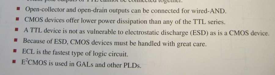
52 Comparison of CMOS and TTL Performance 52
53 Figure An ECL OR/NOR gate circuit. 53
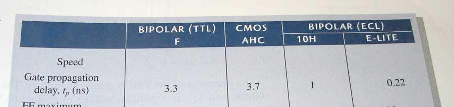
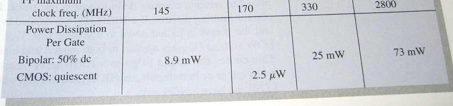
54 Comparison of ECL with TTL and CMOS 54
55 PMOS, NMOS, and E 2 CMOS PMOS - one of the first high density MOS technologies NMOS circuits were developed as processing technology improved E 2 MOS combined the CMOS and NMOS technologies, this is used in the GALs of chapter 7 and 11 55
56 Figure Basic PMOS gate. 56
57 Figure Two NMOS gates. 57
58 Figure An E 2 CMOS cell. 58

59 SUMMARY 59
Copyright 2000 N. AYDIN. All rights reserved. 1
 Electronic Circuits Prof. Nizamettin AYDIN naydin@yildiz.edu.tr http://www.yildiz.edu.tr/~naydin Dr. Gökhan Bilgin gokhanb@ce.yildiz.edu.tr Digital devices Introduction Gate characteristics Logic families
Presented By :- Alok Kumar Lecturer in ECE C.R.Polytechnic, Rohtak
 Presented By :- Alok Kumar Lecturer in ECE C.R.Polytechnic, Rohtak Content - Introduction -2 Feature -3 Feature of BJT -4 TTL -5 MOS -6 CMOS -7 K- Map - Introduction Logic IC ASIC: Application Specific
Digital Electronics. CHAPTER THIRTY TWO. Semiconductor Read-Only Memories
 Digital Electronics. CHAPTER THIRTY TWO Semiconductor Read-Only Memories Introduction Diode circuits, BJT circuits, and MOSFET circuits are used to provide memory semiconductor circuits consisting of both
Latch-Up. Parasitic Bipolar Transistors
 Latch-Up LATCH-UP CIRCUIT Latch-up is caused by an SCR (Silicon Controlled Rectifier) circuit. Fabrication of CMOS integrated circuits with bulk silicon processing creates a parasitic SCR structure. The
This presentation will..
 Component Identification: Digital Introduction to Logic Gates and Integrated Circuits Digital Electronics 2014 This presentation will.. Introduce transistors, logic gates, integrated circuits (ICs), and
DIGITAL ELECTRONICS. Vayu Education of India
 DIGITAL ELECTRONICS ARUN RANA Assistant Professor Department of Electronics & Communication Engineering Doon Valley Institute of Engineering & Technology Karnal, Haryana (An ISO 9001:2008 ) Vayu Education
Product Information. IC Outputs Terms & Definitions
 Product Information IC Outputs Terms & Definitions These terms and their definitions are taken from EIA/JEDEC Standard No. 99-A, Terms, Definitions, and Letter Symbols for Microelectronic Devices, clause
Principles of Digital Techniques PDT (17320) Assignment No State advantages of digital system over analog system.
 Assignment No State advantages of digital system over analog system.") Assignment No. 1 1. State advantages of digital system over analog system. 2. Convert following numbers a. (138.56) 10 = (?) 2 = (?) 8 = (?) 16 b. (1110011.011) 2 = (?) 10 = (?) 8 = (?) 16 c. (3004.06)
Assignment No. 1 1. State advantages of digital system over analog system. 2. Convert following numbers a. (138.56) 10 = (?) 2 = (?) 8 = (?) 16 b. (1110011.011) 2 = (?) 10 = (?) 8 = (?) 16 c. (3004.06)
DIPLOMA COURSE IN ELECTRONICS AND COMMUNICATION ENGINEERING
 Department of Technical Education DIPLOMA COURSE IN ELECTRONICS AND COMMUNICATION ENGINEERING Third Semester Subject: Digital Electronics & Introduction to Microprocessors Contact Hrs/Week:4 Hrs Contact
High-side Power Distribution Switch NCT3521U
 High-side Power Distribution Switch NCT3521U -Table of Content- 1. GENERAL DESCRIPTION...1 2. FEATURES...1 3. APPLICATIONS...2 4. PIN CONFIGURATION AND DESCRIPTION...2 5. TYPICAL APPLICATION CIRCUIT...3
Intro to Logic Gates & Datasheets. Intro to Logic Gates & Datasheets. Introduction to Integrated Circuits. TTL Vs. CMOS Logic
 Intro to Logic Gates & Datasheets Digital Electronics Intro to Logic Gates & Datasheets This presentation will Introduce integrated circuits (ICs). Present an overview of : Transistor-Transistor Logic
Intro to Logic Gates & Datasheets. Digital Electronics
 Intro to Logic Gates & Datasheets Digital Electronics Intro to Logic Gates & Datasheets This presentation will Introduce integrated circuits (ICs). Present an overview of : Transistor-Transistor Logic
National Semiconductor Application Note 368 Larry Wakeman March 1984
 An Introduction to and Comparison of 54HCT 74HCT TTL Compatible CMOS Logic The 54HC 74HC series of high speed CMOS logic is unique in that it has a sub-family of components designated 54HCT 74HCT Generally
CONTENTS CHAPTER 1: NUMBER SYSTEM. Foreword...(vii) Preface... (ix) Acknowledgement... (xi) About the Author...(xxiii)
 Preface... (ix) Acknowledgement... (xi) About the Author...(xxiii)") CONTENTS Foreword...(vii) Preface... (ix) Acknowledgement... (xi) About the Author...(xxiii) CHAPTER 1: NUMBER SYSTEM 1.1 Digital Electronics... 1 1.1.1 Introduction... 1 1.1.2 Advantages of Digital Systems...
CONTENTS Foreword...(vii) Preface... (ix) Acknowledgement... (xi) About the Author...(xxiii) CHAPTER 1: NUMBER SYSTEM 1.1 Digital Electronics... 1 1.1.1 Introduction... 1 1.1.2 Advantages of Digital Systems...
Power IC 용 ESD 보호기술. 구용서 ( Yong-Seo Koo ) Electronic Engineering Dankook University, Korea
 Electronic Engineering Dankook University, Korea") Power IC 용 ESD 보호기술 구용서 ( Yong-Seo Koo ) Electronic Engineering Dankook University, Korea yskoo@dankook.ac.kr 031-8005-3625 Outline Introduction Basic Concept of ESD Protection Circuit ESD Technology Issue
Power IC 용 ESD 보호기술 구용서 ( Yong-Seo Koo ) Electronic Engineering Dankook University, Korea yskoo@dankook.ac.kr 031-8005-3625 Outline Introduction Basic Concept of ESD Protection Circuit ESD Technology Issue
Hours / 100 Marks Seat No.
 17320 21718 3 Hours / 100 Seat No. Instructions (1) All Questions are Compulsory. (2) Answer each next main Question on a new page. (3) Figures to the right indicate full marks. (4) Assume suitable data,
74VHC14 Hex Schmitt Inverter
 74VHC14 Hex Schmitt Inverter General Description June 1993 Revised April 1999 The VHC14 is an advanced high speed CMOS Hex Schmitt Inverter fabricated with silicon gate CMOS technology. It achieves the
CD4023BC Buffered Triple 3-Input NAND Gate
 CD4023BC Buffered Triple 3-Input NAND Gate General Description These triple gates are monolithic complementary MOS (CMOS) integrated circuits constructed with N- and P- channel enhancement mode transistors.
Lecture 20: Package, Power, and I/O
 Introduction to CMOS VLSI Design Lecture 20: Package, Power, and I/O David Harris Harvey Mudd College Spring 2004 1 Outline Packaging Power Distribution I/O Synchronization Slide 2 2 Packages Package functions
CHAPTER 5. Voltage Regulator
 CHAPTER 5 Voltage Regulator In your robot, the energy is derived from batteries. Specifically, there are two sets of batteries wired up to act as voltage sources; a 9V battery, and two 1.5V batteries in
SIDDHARTH INSTITUTE OF ENGINEERING AND TECHNOLOGY :: PUTTUR (AUTONOMOUS) Siddharth Nagar, Narayanavanam Road QUESTION BANK UNIT I
 Siddharth Nagar, Narayanavanam Road QUESTION BANK UNIT I") SIDDHARTH INSTITUTE OF ENGINEERING AND TECHNOLOGY :: PUTTUR (AUTONOMOUS) Siddharth Nagar, Narayanavanam Road 517583 QUESTION BANK Subject with Code : DICD (16EC5703) Year & Sem: I-M.Tech & I-Sem Course
SIDDHARTH INSTITUTE OF ENGINEERING AND TECHNOLOGY :: PUTTUR (AUTONOMOUS) Siddharth Nagar, Narayanavanam Road 517583 QUESTION BANK Subject with Code : DICD (16EC5703) Year & Sem: I-M.Tech & I-Sem Course
EE 434 Lecture 30. Logic Design
 EE 434 Lecture 30 Logic Design Review from last time: Hierarchical nalog Design Domains: Top Behavioral: Structural: Physical Bottom Up Design Top Down Design Bottom Review from last time: Hierarchical
Features. Applications. MIC4126/27/28 Block Diagram
 Dual 1.5A-Peak Low-Side MOSFET Drivers in Advanced Packaging General Description The MIC4126, MIC4127, and MIC4128 family are highlyreliable dual 1.5A low-side MOSFET drivers fabricated on Micrel s BiCMOS/DMOS
3. The high voltage level of a digital signal in positive logic is : a) 1 b) 0 c) either 1 or 0
 1 b) 0 c) either 1 or 0") 1. The number of level in a digital signal is: a) one b) two c) four d) ten 2. A pure sine wave is : a) a digital signal b) analog signal c) can be digital or analog signal d) neither digital nor analog
1. The number of level in a digital signal is: a) one b) two c) four d) ten 2. A pure sine wave is : a) a digital signal b) analog signal c) can be digital or analog signal d) neither digital nor analog
Voltage Translation (5 V, 3.3 V, 2.5 V, 1.8 V), Switching Standards, and Bus Contention
, Switching Standards, and Bus Contention") Voltage Translation (5 V, 3.3 V, 2.5 V, 1.8 V), Switching Standards, and Bus Contention SCYA006 September 1999 1 IMPORTANT NOTICE Texas Instruments and its subsidiaries (TI) reserve the right to make changes
Voltage Translation (5 V, 3.3 V, 2.5 V, 1.8 V), Switching Standards, and Bus Contention SCYA006 September 1999 1 IMPORTANT NOTICE Texas Instruments and its subsidiaries (TI) reserve the right to make changes
74VHC132 Quad 2-Input NAND Schmitt Trigger
 74VHC132 Quad 2-Input NAND Schmitt Trigger General Description The VHC132 is an advanced high speed CMOS 2-input NAND Schmitt Trigger Gate fabricated with silicon gate CMOS technology. It achieves the
4. Hot Socketing and Power-On Reset in MAX V Devices
 December 2010 MV51004-1.0 4. Hot Socketing and Power-On Reset in MAX V Devices MV51004-1.0 This chapter provides information about hot-socketing specifications, power-on reset (POR) requirements, and their
Introduction to ICs and Transistor Fundamentals
 Introduction to ICs and Transistor Fundamentals A Brief History 1958: First integrated circuit Flip-flop using two transistors Built by Jack Kilby at Texas Instruments 2003 Intel Pentium 4 mprocessor (55
TD62382AP,TD62382AF TD62382AP/AF 8CH LOW INPUT ACTIVE SINK DRIVER FEATURES PIN CONNECTION (TOP VIEW) SCHEMATICS (EACH DRIVER)
 SCHEMATICS (EACH DRIVER)") TOSHIBA BIPOLAR DIGITAL INTEGRATED CIRCUIT SILICON MONOLITHIC TD62382AP,TD62382AF TD62382AP/AF 8CH LOW INPUT ACTIVE SINK DRIVER The TD62382AP / AF are non inverting transistor array which are comprised
TOSHIBA BIPOLAR DIGITAL INTEGRATED CIRCUIT SILICON MONOLITHIC TD62382AP,TD62382AF TD62382AP/AF 8CH LOW INPUT ACTIVE SINK DRIVER The TD62382AP / AF are non inverting transistor array which are comprised
INTEGRATED CIRCUITS APPLICATION NOTE. AN252 Live Insertion Aspects of Philips Logic Families. Author: Mike Magdaluyo July Philips Semiconductors
 INTEGRATED CIRCUITS APPLICATION NOTE Live Insertion Aspects of Philips Logic Families Author: Mike Magdaluyo July 1999 Philips Semiconductors Author: Mike Magdaluyo, Philips Semiconductors, Sunnyvale INTRODUCTION
EXPERIMENT 6. CMOS INVERTERS AND CMOS LOGIC CIRCUITS
 EXPERIMENT 6. CMOS INVERTERS AND CMOS LOGIC CIRCUITS I. Introduction I.I Objectives In this experiment, you will analyze the voltage transfer characteristics (VTC) and the dynamic response of the CMOS
Sketch A Transistor-level Schematic Of A Cmos 3-input Xor Gate
 Sketch A Transistor-level Schematic Of A Cmos 3-input Xor Gate DE09 DIGITALS ELECTRONICS 3 (For Mod-m Counter, we need N flip-flops (High speeds are possible in ECL because the transistors are used in
Sense Amplifiers 6 T Cell. M PC is the precharge transistor whose purpose is to force the latch to operate at the unstable point.
 Announcements (Crude) notes for switching speed example from lecture last week posted. Schedule Final Project demo with TAs. Written project report to include written evaluation section. Send me suggestions
Advanced BiCMOS features
 Advanced BiCMOS Features With the advent of the newer BiCMOS and 3 volt technologies, product feature sets have been enhanced from the standard features found in previous logic families. With the newer
CD4010C Hex Buffers (Non-Inverting)
") Hex Buffers (Non-Inverting) General Description The CD4010C hex buffers are monolithic complementary MOS (CMOS) integrated circuits. The N- and P-channel enhancement mode transistors provide a symmetrical
Hex Buffers (Non-Inverting) General Description The CD4010C hex buffers are monolithic complementary MOS (CMOS) integrated circuits. The N- and P-channel enhancement mode transistors provide a symmetrical
Number Systems UNIT. Learning Objectives. 1.0 Introduction
 UNIT 1 Number Systems Learning Objectives To study Binary, Octal, Hexadecimal, Decimal number systems. Conversion of Binary to Octal, Binary to decimal, Binary to Hexa decimal and Conversion. Binary Addition,
E40M. MOS Transistors, CMOS Logic Circuits, and Cheap, Powerful Computers. M. Horowitz, J. Plummer, R. Howe 1
 E40M MOS Transistors, CMOS Logic Circuits, and Cheap, Powerful Computers M. Horowitz, J. Plummer, R. Howe 1 Reading Chapter 4 in the reader For more details look at A&L 5.1 Digital Signals (goes in much
AN2408 Application note
 Application note 900mA standalone linear Li-Ion battery charger with thermal regulation Introduction One way to minimize the size and complexity of a battery charger is to use a linear-type charger. The
Quad GTL/GTL+ to LVTTL/TTL bidirectional non-latched translator
 Quad GTL/GTL+ to LVTTL/TTL bidirectional non-latched translator Rev. 07 3 February 2009 Product data sheet 1. General description The is a quad translating transceiver designed for 3.3 V system interface
3. Implementing Logic in CMOS
 3. Implementing Logic in CMOS 3. Implementing Logic in CMOS Jacob Abraham Department of Electrical and Computer Engineering The University of Texas at Austin VLSI Design Fall 27 September, 27 ECE Department,
Chapter 2. Boolean Algebra and Logic Gates
 Chapter 2. Boolean Algebra and Logic Gates Tong In Oh 1 Basic Definitions 2 3 2.3 Axiomatic Definition of Boolean Algebra Boolean algebra: Algebraic structure defined by a set of elements, B, together
TD62384APG,TD62384AFG TD62385APG,TD62385AFG
 TOSHIBA BIPOLAR DIGITAL INTEGRATED CIRCUIT SILICON MONOLITHIC TD62384APG,TD62384AFG TD62385APG,TD62385AFG 8CH LOW INPUT ACTIVE DARLINGTON SINK DRIVER The TD62384APG / AFG and TD62385APG / AFG are non inverting
PLCIO2 Programmable Logic Controller Updated 3/26/10
 Overview: PLCIO2 Programmable Logic Controller Updated 3/26/10 PLCIO2 is a programmable logic controller which provides: 35 Inputs (bipolar, with a choice of 5 or 24) 39 Outputs (20SPST, 2 SPDT, 17 open
74ALVC132 Low Voltage Quad 2-Input NAND Gate with Schmitt Trigger Inputs and 3.6V Tolerant Inputs and. and Outputs. General Description.
 74ALC132 Low oltage Quad 2-Input NAND Gate with Schmitt Trigger Inputs and 3.6 Tolerant Inputs and General Description The ALC132 contains four 2-input NAND gates with Schmitt Trigger Inputs. The pin configuration
Texas Instruments Solution for Undershoot Protection for Bus Switches
 Application Report SCDA007 - APRIL 2000 Texas Instruments Solution for Undershoot Protection for Bus Switches Nadira Sultana and Chris Graves Standard Linear & Logic ABSTRACT Three solutions for undershoot
8-CHANNEL SATURATED SINK DRIVER
 Data Sheet 29320B UDNA Developed for use with low-voltage LED and incandescent displays requiring low output saturation voltage, the UDNA and ASLW meet many interface needs, including those exceeding the
74VCX00 Low Voltage Quad 2-Input NAND Gate with 3.6V Tolerant Inputs and Outputs
 74CX00 Low oltage Quad 2-Input NAND Gate with 3.6 Tolerant Inputs and Outputs General Description The CX00 contains four 2-input NAND gates. This product is designed for low voltage (1.65 to 3.6) CC applications
CMOS INVERTER LAYOUT TUTORIAL
 PRINCESS SUMAYA UNIVERSITY FOR TECHNOLOGY CMOS INVERTER LAYOUT TUTORIAL We will start the inverter by drawing a PMOS. The first step is to draw a poly layer. Click on draw a rectangle and choose the poly
VARTA Powercaps HVC Series
 HVC Series HVC 90F Discharge Information - Constant Power Discharge - Constant Current Discharge - Energy versus Temperature - ESR (DC) versus Temperature & important general notes to discharge 2017-08-09,
Operating Requirements
 Operating Requirements for Altera Devices January 1998, ver. 8 Data Sheet Introduction Altera devices combine unique programmable logic architectures with advanced CMOS processes to provide exceptional
Boolean Algebra and Logic Gates
 Boolean Algebra and Logic Gates Binary logic is used in all of today's digital computers and devices Cost of the circuits is an important factor Finding simpler and cheaper but equivalent circuits can
Turning Ideas Into Reality ABCircuits POB 123 New Hill NC (919) C922-SO IC
 C922-SO IC") ABCircuits www.abcircuits.com POB 123 New Hill 27562 (919) 290-7104 74C922-SO IC Keyboard / Keypad Encoder for up to 16 switches MM74C922 Replacement IC General Description The 74C922-SO is designed as
ABCircuits www.abcircuits.com POB 123 New Hill 27562 (919) 290-7104 74C922-SO IC Keyboard / Keypad Encoder for up to 16 switches MM74C922 Replacement IC General Description The 74C922-SO is designed as
Chap-2 Boolean Algebra
 Chap-2 Boolean Algebra Contents: My name Outline: My position, contact Basic information theorem and postulate of Boolean Algebra. or project description Boolean Algebra. Canonical and Standard form. Digital
Low Voltage Bandgap References and High PSRR Mechanism
 Low Voltage Bandgap References and High PSRR Mechanism Vahe Arakelyan 2nd year Master Student Synopsys Armenia Educational Department, State Engineering University of Armenia Moscow March 21-24, 2011 Outline
ESE 570 Cadence Lab Assignment 2: Introduction to Spectre, Manual Layout Drawing and Post Layout Simulation (PLS)
") ESE 570 Cadence Lab Assignment 2: Introduction to Spectre, Manual Layout Drawing and Post Layout Simulation (PLS) Objective Part A: To become acquainted with Spectre (or HSpice) by simulating an inverter,
ESE 570 Cadence Lab Assignment 2: Introduction to Spectre, Manual Layout Drawing and Post Layout Simulation (PLS) Objective Part A: To become acquainted with Spectre (or HSpice) by simulating an inverter,
SS1438 Unipolar Hall Switch
 Features and Benefits Wide operating voltage range from 2.5V to 24V Medium sensitivity CMOS technology Chopper-stabilized amplifier stage Superior temperature stability Extremely low switchpoint drift
CS MARKING DIAGRAM ORDERING INFORMATION. Figure 1. Block Diagram TO 220 FIVE LEAD TQ SUFFIX CASE 314D
 The CS824 is a fast, PNP high side driver capable of delivering up to ma into a resistive or inductive load in harsh automotive or industrial environments. An internal flyback diode clamp is incorporated
TABLE OF CONTENTS 1.0 PURPOSE INTRODUCTION ESD CHECKS THROUGHOUT IC DESIGN FLOW... 2
 TABLE OF CONTENTS 1.0 PURPOSE... 1 2.0 INTRODUCTION... 1 3.0 ESD CHECKS THROUGHOUT IC DESIGN FLOW... 2 3.1 PRODUCT DEFINITION PHASE... 3 3.2 CHIP ARCHITECTURE PHASE... 4 3.3 MODULE AND FULL IC DESIGN PHASE...
Analog and Telecommunication Electronics
 Politecnico di Torino - ICT School Analog and Telecommunication Electronics F4 - Actuator driving» Driving BJT switches» Driving MOS-FET» SOA and protection» Smart switches 30/05/2014-1 ATLCE - F4-2011
RAJIV GANDHI COLLEGE OF ENGINEERING AND TECHNOLOGY
 RAJIV GANDHI COLLEGE OF ENGINEERING AND TECHNOLOGY DEPARTMENT OF ELECTRICAL & ELECTRONICS ENGINEERING QUESTION BANK EE T34 - Electronic Devices and Circuits II YEAR / III SEMESTER RGCET 1 UNIT-I 1. How
TD62M8600FG TD62M8600FG 8CH LOW SATURATION VOLTAGE SOURCE DRIVER FEATURES SCHEMATICS PIN CONNECTION (TOP VIEW)
") TOSHIBA BIPOLAR DIGITAL INTEGRATED CIRCUIT MULTI CHIP TD62M8600FG TD62M8600FG 8CH LOW SATURATION VOLTAGE SOURCE DRIVER TD62M8600FG is Multi Chip IC incorporates 8 low saturation discrete transistors equipped
TOSHIBA BIPOLAR DIGITAL INTEGRATED CIRCUIT MULTI CHIP TD62M8600FG TD62M8600FG 8CH LOW SATURATION VOLTAGE SOURCE DRIVER TD62M8600FG is Multi Chip IC incorporates 8 low saturation discrete transistors equipped
SOT553/563 Launch Packet
 Left-to-right: SOD523, SC75, SOT563, SOT23 SOT553/563 Launch Packet June 2003 1 ON Semiconductor Offering the widest SOT553/556 portfolio SC88 / SOT 363 2 x SC70 SOT553 / SOT563 2 Package Size Comparison
Basic Interface Techniques for the CRD155B
 Basic Interface Techniques for the CRD155B April 2001, ver. 1.10 Application Note 101 Introduction This application note contains basic information about interfacing external circuitry to computer I/O
Design of Low Power Wide Gates used in Register File and Tag Comparator
 www..org 1 Design of Low Power Wide Gates used in Register File and Tag Comparator Isac Daimary 1, Mohammed Aneesh 2 1,2 Department of Electronics Engineering, Pondicherry University Pondicherry, 605014,
ECE484 VLSI Digital Circuits Fall Lecture 01: Introduction
 ECE484 VLSI Digital Circuits Fall 2017 Lecture 01: Introduction Adapted from slides provided by Mary Jane Irwin. [Adapted from Rabaey s Digital Integrated Circuits, 2002, J. Rabaey et al.] CSE477 L01 Introduction.1
Hours / 100 Marks Seat No.
 17333 13141 3 Hours / 100 Seat No. Instructions (1) All Questions are Compulsory. (2) Answer each next main Question on a new page. (3) Illustrate your answers with neat sketches wherever necessary. (4)
Page 1 ATLCE - G2 17/06/2013. Analog and Telecommunication Electronics 2013 DDC 1. Politecnico di Torino - ICT School
 Politecnico di Torino - CT School Lesson G2: Linear voltage regulators Analog and Telecommunication Electronics G2 - Linear voltage regulators» Shunt regulators» Series regulator» ntegrated regulators»ldo
Boolean Algebra. BME208 Logic Circuits Yalçın İŞLER
 Boolean Algebra BME28 Logic Circuits Yalçın İŞLER islerya@yahoo.com http://me.islerya.com 5 Boolean Algebra /2 A set of elements B There exist at least two elements x, y B s. t. x y Binary operators: +
2.5 A Output Current, IGBT Drive Optocoupler with Desaturation Detection and Isolated Fault Sensing. Featured Fairchild Product/s: FOD8316
 User Guide for FEBFOD8316 Evaluation Board 2.5 A Output Current, IGBT Drive Optocoupler with Desaturation Detection and Isolated Fault Sensing Featured Fairchild Product/s: FOD8316 Direct questions or
Lab 16: Data Busses, Tri-State Outputs and Memory
 Lab 16: Data Busses, Tri-State Outputs and Memory UC Davis Physics 116B Rev. 0.9, Feb. 2006 1 Introduction 1.1 Data busses Data busses are ubiquitous in systems which must communicate digital data. Examples
New Enhanced Possibilities of Netlist Comparison in Guardian LVS
 Application Note New Enhanced Possibilities of Netlist Comparison in Guardian LVS 1. Introduction The Guardian LVS (Layout versus Schematic) netlist comparison tool compares two SPICE netlists. One of
ESD Protection Design With Low-Capacitance Consideration for High-Speed/High- Frequency I/O Interfaces in Integrated Circuits
 Recent Patents on Engineering 2007, 1, 000-000 1 ESD Protection Design With Low-Capacitance Consideration for High-Speed/High- Frequency I/O Interfaces in Integrated Circuits Ming-Dou Ker* and Yuan-Wen
Lecture (05) Boolean Algebra and Logic Gates
 Boolean Algebra and Logic Gates") Lecture (05) Boolean Algebra and Logic Gates By: Dr. Ahmed ElShafee ١ Minterms and Maxterms consider two binary variables x and y combined with an AND operation. Since eachv ariable may appear in either
Lecture (05) Boolean Algebra and Logic Gates By: Dr. Ahmed ElShafee ١ Minterms and Maxterms consider two binary variables x and y combined with an AND operation. Since eachv ariable may appear in either
SIDDHARTH GROUP OF INSTITUTIONS :: PUTTUR (AUTONOMOUS) Siddharth Nagar, Narayanavanam Road QUESTION BANK (DESCRIPTIVE) UNIT I
 Siddharth Nagar, Narayanavanam Road QUESTION BANK (DESCRIPTIVE) UNIT I") QUESTION BANK 2017 SIDDHARTH GROUP OF INSTITUTIONS :: PUTTUR (AUTONOMOUS) Siddharth Nagar, Narayanavanam Road 517583 QUESTION BANK (DESCRIPTIVE) Subject with Code : Basic Electronic Devices (16EC401) Year
QUESTION BANK 2017 SIDDHARTH GROUP OF INSTITUTIONS :: PUTTUR (AUTONOMOUS) Siddharth Nagar, Narayanavanam Road 517583 QUESTION BANK (DESCRIPTIVE) Subject with Code : Basic Electronic Devices (16EC401) Year
11 Patent Number: 5,519,242 Avery 45) Date of Patent: May 21, 1996
 Date of Patent: May 21, 1996") United States Patent (19) I I USOO5519242A 11 Patent Number: 5,519,242 Avery 45) Date of Patent: May 21, 1996 54 ELECTROSTATIC DISCHARGE 5,357,126 10/1994 Jimenez... 257/173 PROTECTION CIRCUIT FOR A NMOS
United States Patent (19) I I USOO5519242A 11 Patent Number: 5,519,242 Avery 45) Date of Patent: May 21, 1996 54 ELECTROSTATIC DISCHARGE 5,357,126 10/1994 Jimenez... 257/173 PROTECTION CIRCUIT FOR A NMOS
SS3144 Unipolar Hall-Effect Digital Switch
 Features and Benefits 4.5V to 24V Operation -40 to 150 Superior temperature operation Bipolar technology Open-collector 25 ma output Reverse battery protection Small Size-SOT23 3L or SIP 3L Solid-state
Data Sheet IHD 260/660 Dual Channel SCALE IGBT Driver Core
 Data Sheet IHD 260/660 Dual Channel SCALE IGBT Driver Core A successor to the IHD 215/280/680 dual-gate driver cores for 1200V and 1700V IGBTs The IHD 260 and IHD 660 (short IHDx60) are highly-integrated
VP603. CRT Display Video Output Amplifier: High-Voltage, Wideband Amplification
 Ordering number : EN5542A Wideband Output Module (Video Pack) VP603 CRT Display Video Output Amplifier: High-Voltage, Wideband Amplification Function Three-channel video output circuit for CRT displays
Prepared by: Jim Lepkowski ON Semiconductor
 Application Hints for Transient Voltage Suppression Diode Circuits Prepared by: Jim Lepkowski ON Semiconductor APPLICATION NOTE INTRODUCTION Transient Voltage Suppression (TVS) diodes provide a simple
Digital Integrated Circuits A Design Perspective. Jan M. Rabaey
 Digital Integrated Circuits A Design Perspective Jan M. Rabaey Outline (approximate) Introduction and Motivation The VLSI Design Process Details of the MOS Transistor Device Fabrication Design Rules CMOS
Lab. Course Goals. Topics. What is VLSI design? What is an integrated circuit? VLSI Design Cycle. VLSI Design Automation
 Course Goals Lab Understand key components in VLSI designs Become familiar with design tools (Cadence) Understand design flows Understand behavioral, structural, and physical specifications Be able to
Embedded Systems and Software
 Embedded Systems and Software Lecture 12 Some Hardware Considerations Hardware Considerations Slide 1 Logic States Digital signals may be in one of three states State 1: High, or 1. Using positive logic
ECE 261: Full Custom VLSI Design
 ECE 261: Full Custom VLSI Design Prof. James Morizio Dept. Electrical and Computer Engineering Hudson Hall Ph: 201-7759 E-mail: jmorizio@ee.duke.edu URL: http://www.ee.duke.edu/~jmorizio Course URL: http://www.ee.duke.edu/~jmorizio/ece261/261.html
TUTORIAL II ECE 555 / 755 Updated on September 11 th 2006 CADENCE LAYOUT AND PARASITIC EXTRACTION
 TUTORIAL II ECE 555 / 755 Updated on September 11 th 2006 CADENCE LAYOUT AND PARASITIC EXTRACTION After finishing a schematic of your design (Tutorial-I), the next step is creating masks which are for
DS232A Dual RS-232 Transmitter/Receiver
 Dual RS-232 Transmitter/Receiver www.dalsemi.com FEATURES Compatible with LT1181A and MAX232A High data rate - 250 kbits/sec under load 16-pin DIP or SOIC package 20-pin TSSOP package for height restricted
MADR TR. SPDT PIN Diode Driver Rev. V3. Features. Functional Block Diagram. Description. Pin Configuration. Ordering Information
 Features Moderate Speed, CMOS Technology (25 ns) Complementary Outputs High Drive Current Capability (± 50 ) Low Current Consumption Plastic SOIC Body for SMT Applications Tape and Reel Packaging Available
SS443 Unipolar Hall-Effect Digital Switch
 Features and Benefits 4.5V to 24V Operation -40 to 150 Superior temperature operation Bipolar technology Open-collector 25 ma output Reverse battery protection Small Size-SOT23 3L and SIP 3L Solid-state
SN54ALS20A, SN54AS20, SN74ALS20A, SN74AS20 DUAL 4-INPUT POSITIVE-NAND GATES
 Package Options Include Plastic Small-Outline (D) Packages, Ceramic Chip Carriers (FK), and Standard Plastic (N) and Ceramic (J) 300-mil DIPs description These devices contain two independent -input positive-nand
RS485 3 click. How does it work? PID: MIKROE-2821
 RS485 3 click PID: MIKROE-2821 RS485 3 click is an RS422/485 transceiver Click board, which can be used as an interface between the TTL level UART and the RS422/485 communication bus. It features a full-duplex
NanoBoard MIDI Interface
 NanoBoard 3000 - MIDI Interface Frozen Content Mod ifi ed by Adm in on Nov 6, 201 3 The NanoBoard 3000 caters for transmission and reception of signals in accordance with the MIDI (Musical Instrument Digital
MC74C Digit BCD Display Controller/Driver. General Description. Ordering Code: Connection Diagram. Features. Version 1.0
 6-Digit BCD Display Controller/Driver General Description The display controllers are interface elements, with memory, that drive a 6-digit, 8-segment LED display. The display controllers receive data
END-TERM EXAMINATION
 (Please Write your Exam Roll No. immediately) END-TERM EXAMINATION DECEMBER 2006 Exam. Roll No... Exam Series code: 100919DEC06200963 Paper Code: MCA-103 Subject: Digital Electronics Time: 3 Hours Maximum
L293 QUADRUPLE HALF-H DRIVER
 QUDRUPE F- DRIVER SRS005 SEPTEMBER 8 REVISED MY 0 - Current Capability Per Driver Pulsed Current - Driver Wide Supply Voltage Range: 4.5 V to V Separate -ogic Supply NE Package Designed for eat Sinking
E85: Digital Design and Computer Engineering Lab 1: Electrical Characteristics of Logic Gates
 E85: Digital Design and Computer Engineering Lab 1: Electrical Characteristics of Logic Gates Objective The purpose of this lab is to become comfortable with logic gates as physical objects, to interpret
HM9708 HM9708. Battery-Powered Equipment Motherboard USB Power Switch USB Device Power Switch Hot-Plug Power Supplies Battery-Charger Circuits DC+ VIN
 200mΩ Power Distribution Switches Features 200mΩ Typ. High-Side MOSFET 0.8A Current Limit (V IN =3.0V) Wide Input Voltage Range: 2V ~ 5.5V Soft Start Thermal Protection Small SOT-23-5 Package Minimizes
Type Version Ordering Code Package PEB 2025-N V 1.5 Q67100-H6300 P-LCC-28-R (SMD) PEB 2025-P V 1.5 Q67100-H6241 P-DIP-22
 PEB 2025-P V 1.5 Q67100-H6241 P-DIP-22") ISDN Exchange Power Controller (IEPC) PEB 2025 CMOS IC Features Supplies power to up to four transmission lines CCITT recommendations compatible for power feed at the S interface Each line is individually
ISDN Exchange Power Controller (IEPC) PEB 2025 CMOS IC Features Supplies power to up to four transmission lines CCITT recommendations compatible for power feed at the S interface Each line is individually
Reversible motor driver
 Reversible motor driver The BA6289F and BA6417F are reversible-motor drivers, with an output current of 600mA for the former and 1A for the latter. Two logic inputs allow four output modes: forward, reverse,
GreenFET TM High Voltage Gate Driver CC D Q-PUMP + _. Timing & Logic. Discharge
 GreenFET TM High Voltage Gate Driver Features 5V ±5% Power supply SLG55021 Drain Voltage Range 1.0V to 20V Internal Gate Voltage Charge Pump Controlled Turn on Delay Controlled Load Discharge Rate Controlled
OVERVOLTAGE SENSING CIRCUIT
 This overvoltage protection circuit (OVP) protects sensitive electronic circuitry from overvoltage transients or regulator failures when used in conjunction with an external crowbar SCR. The device senses
RAJIV GANDHI COLLEGE OF ENGINEERING AND TECHNOLOGY DEPARTMENT OF ECE QUESTION BANK- EDC SEMESTER - III UNIT I : SEMICONDUCTOR DIODS PART A
 RAJIV GANDHI COLLEGE OF ENGINEERING AND TECHNOLOGY DEPARTMENT OF ECE QUESTION BANK- EDC SEMESTER - III UNIT I : SEMICONDUCTOR DIODS 1. Define Electronics. 2. What is meant by forbidden energy gap. 3. Classify