Graphics: Alexandra Nolte, Gesine Marwedel, Universität Dortmund. RTL Synthesis
|
|
|
- Teresa Garrison
- 5 years ago
- Views:
Transcription

1 Graphics: Alexandra Nolte, Gesine Marwedel, 2003 Universität Dortmund RTL Synthesis
2 Purpose of HDLs Purpose of Hardware Description Languages: Capture design in Register Transfer Language form i.e. All registers specified Use to simulate design so as to verify correctness Pass through Synthesis tool to obtain reasonably optimal gate-level design that meets timing Design productivity Automatic synthesis Capture design as RTL instead of schematic Reduces time to create gate level design by an order of magnitude Synthesis FOCUS OF THIS LECTURE Basically, a Boolean Combinational Logic optimizer that is timing aware
3 Hardware Implementations HDLs can be compiled to semi-custom and programmable hardware implementations Full Custom Semi- Custom Programmable Manual VLSI Standard Cell Gate Array FPGA less work, faster time to market implementation efficiency PLD 3
4 ASIC Application Specific Integrated Circuit A chip designed to perform a particular operation as opposed to General Purpose integrated circuits An ASIC is generally NOT software programmable to perform a wide variety of different tasks An ASIC will often have an embedded CPU to manage suitable tasks An ASIC may be implemented as an FPGA Sometimes considered a separate category
5 Examples of ASICs Video processor to decode or encode MPEG-2 digital TV signals Low power dedicated DSP/controller /convergence device for mobile phones Encryption processor for security Many examples of graphics chips Network processor for managing packets, traffic flow, etc.


6 ASIC Styles Full Custom ASICs Every transistor is designed and drawn by hand Typically only way to design analog portions of ASICs Gives the highest performance but the longest design time Full set of masks required for fabrication
 Standard-Cell-Based ASICs or Cell Based IC (CBIC) or semi-custom Standard Cells are custom designed and")

7 ASIC Styles (Contd.) Standard-Cell-Based ASICs or Cell Based IC (CBIC) or semi-custom Standard Cells are custom designed and then inserted into a library These cells are then used in the design by being placed in rows and wired together using place and route CAD tools Some standard cells, such as RAM and ROM cells, and some datapath cells (e.g. a multiplier) are tiled together to create macrocells D-flip-flop: NOR gate:
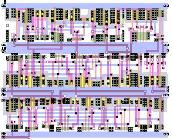
8 Standard Cell ASICs Sample ASIC floorplan: Standard Cell designs are usually synthesized from an RTL (Register Transfer Language) description of the design Intellectual Property Blocks (IPs) are often used to decrease Time to Market Hard IP (like SRAM): Technology Dependent, GDSII and libs Soft IP (DW library): Tech independent, delivered as RTL, with synthesis and verification scripts Standard-cell area (Soft Macro) Fixed blocks (Hard Macros) I/O cells

9 Standard Cell ASICs 3D view 2D view

10 Standard Cell ASICs
11

12 Logic Synthesis Automatic synthesis is used to turn the RTL into a gatelevel description ie. AND, OR gates, etc. Chip-test features are usually inserted at this point Gate level design verified for correctness Output of synthesis is a net-list i.e. List of logic gates and their implied connections NOR2 U36 (.Y(n107),.A0(n109),.A1(\value[2] ) ); NAND2 U37 (.Y(n109),.A0(n105),.A1(n103) ); NAND2 U38 (.Y(n114),.A0(\value[1] ),.A1(\value[0] ) ); NOR2 U39 (.Y(n115),.A0(\value[3] ),.A1(\value[2] ) );
 Synthesis HDL Translation Mapping Static Timing (DC/DCT/PC/PT) Formal Equivalence (FM) Power Analysis")
13 Logic Synthesis Timing/Logic Library IP Library(DW) Physical Library RTL Timing Constraints Floorplan Synthesis (DC, DCT) residue = 16 h0000; if (high_bits == 2 b10) else residue = state_table[index]; state_table[index] = 16 h0000; Hardware Description Language (HDL) Synthesis HDL Translation Mapping Static Timing (DC/DCT/PC/PT) Formal Equivalence (FM) Power Analysis (DC/DCT/PC/PT-PX) Static Timing Placement Routing Estimation Meets Spec? No Optimization Design Rule Fixing Scan-Ready Netlist DFT Yes Target Technology (standard cells)
14 Floorplanning Corner cell I/O cell P/G buses Pad Die edge Bonding wire SOFT Macro Digital core Std Cell PLL RAM Leadframe Die Bonding Wire Core Area Resin mould Leadframe
 or a configuration")

15 Placement Physical Design tools used to turn the gate-level design into a set of chip masks (for photolithography) or a configuration file for downloading to an FPGA Floorplanning and Power Planning Positioning of major functions Placement of the Standard cells Gates arranged in rows

16 Clock Tree Synthesis (CTS) Clock and buffer Insertion Distribute clocks to cells and locate buffers for use as amplifiers in long wires


17 Routing Routing Logic Cells wired together Clock Routing Global Routing Detailed routing
18 Signoff & Chip Finishing Route Database Timing/Logic Library Hard Macro Library Physical Library Chip Finishing (Astro) Metal Fill Chip Finishing Double Via Insertion Filler Cell Insertion Critical Area Optimization Route Optimization STA with SI and SSTA for variations Antenna Fixing Route DRC Fixing IR drop and EM Analysis Design Rule Fixing Static Timing (PT/Star-RCXT) Formal Equiv (FM) Power Analysis (PTPX/PrimeRail) Route DRC (Hercules) LVS (Hercules) GDSII Meets Spec? Yes Mask Synthesis No GDSII
19 Synthesis/Mapping/Optimization Synthesis Converting the RTL into a generic logic netlist Mapping Mapping the generic netlist into standard cells from the core library Optimisation Optimising the logic to meet timing, area and power constraints RTL module counter( input clk, rstn, load, input [1:0] in, output reg [1:0] out); clk) if (!rstn) out <= 2'b0; else if (load) out <= in; else out <= out + 1; endmodule Constraints Synthesis Netlist module counter ( clk, rstn, load, in, out ); input [1:0] in; output [1:0] out; input clk, rstn, load; wire N6, N7, n5, n6, n7, n8; HDDFFPQ1 out_reg_1 (.D(N7),.CK(clk),.Q(out[1])); HDDFFPQ1 out_reg_0 (.D(N6),.CK(clk),.Q(out[0])); HDNAN2DL U8 (.A1(out[0]),.A2(n5),.Z(n8)); HDNAN2DL U9 (.A1(n5),.A2(n7),.Z(n6)); HDINVDL U10 (.A(load),.Z(n5)); HDOA211DL U11 (.A1(in[0]),.A2(n5),.B(rstn),.C(n8),.Z(N6)); HDOA211DL U12 (.A1(in[1]),.A2(n5),.B(rstn),.C(n6),.Z(N7)); HDEXNOR2DL U13 (.A1(out[1]),.A2(out[0]),.Z(n7)); endmodule 19
20 Synchronous RTL design Pseudo outputs Pseudo inputs Primary outputs Primary inputs
21 RTL Synthesis RTL file Gate level select Sel begin if(select= 1 ) a Xor pin1 q q<= a xor b; b else MUX q<=a and b; end And pin0
22 clk, posedge reset) begin if(reset== 1 b1) q<= 0; else q<=a or b; end Sequential parts
23 Synthesis Recap The RTL The Register Transfer Level code can be written in VHDL, Verilog, SystemVerilog, or even SystemC RTL is a particular coding style, which defines io s, clocked sequential statements, and combinational logic RTL module counter( input clk, rstn, load, input [1:0] in, output reg [1:0] out); clk) if (!rstn) out <= 2'b0; else if (load) out <= in; else out <= out + 1; endmodule Constraints Synthesis Netlist module counter ( clk, rstn, load, in, out ); input [1:0] in; output [1:0] out; input clk, rstn, load; wire N6, N7, n5, n6, n7, n8; HDDFFPQ1 out_reg_1 (.D(N7),.CK(clk),.Q(out[1])); HDDFFPQ1 out_reg_0 (.D(N6),.CK(clk),.Q(out[0])); HDNAN2DL U8 (.A1(out[0]),.A2(n5),.Z(n8)); HDNAN2DL U9 (.A1(n5),.A2(n7),.Z(n6)); HDINVDL U10 (.A(load),.Z(n5)); HDOA211DL U11 (.A1(in[0]),.A2(n5),.B(rstn),.C(n8),.Z(N6)); HDOA211DL U12 (.A1(in[1]),.A2(n5),.B(rstn),.C(n6),.Z(N7)); HDEXNOR2DL U13 (.A1(out[1]),.A2(out[0]),.Z(n7)); endmodule 23
24 Synthesis Recap The Netlist The netlistis always written in verilogformat Other languages are not supported by the tools, or only poorly supported by the tools. Specifying the top level interface, Connectivity between library instances and Logical hierarchy (Usually) RTL module counter( input clk, rstn, load, input [1:0] in, output reg [1:0] out); clk) if (!rstn) out <= 2'b0; else if (load) out <= in; else out <= out + 1; endmodule Constraints Synthesis Netlist module counter ( clk, rstn, load, in, out ); input [1:0] in; output [1:0] out; input clk, rstn, load; wire N6, N7, n5, n6, n7, n8; HDDFFPQ1 out_reg_1 (.D(N7),.CK(clk),.Q(out[1])); HDDFFPQ1 out_reg_0 (.D(N6),.CK(clk),.Q(out[0])); HDNAN2DL U8 (.A1(out[0]),.A2(n5),.Z(n8)); HDNAN2DL U9 (.A1(n5),.A2(n7),.Z(n6)); HDINVDL U10 (.A(load),.Z(n5)); HDOA211DL U11 (.A1(in[0]),.A2(n5),.B(rstn),.C(n8),.Z(N6)); HDOA211DL U12 (.A1(in[1]),.A2(n5),.B(rstn),.C(n6),.Z(N7)); HDEXNOR2DL U13 (.A1(out[1]),.A2(out[0]),.Z(n7)); endmodule 24
25
26
27
28
29
30
31
32
33
34
35

36 Clock Insertion delay T period T ck T d T su T id-launch T id-capture = Target clock period = Popagation delay of launching flip-flop = Propagation delay of combinational cells = Setup time of capture flip-flop = Clock insertion delay of launch path = Clock insertion delay of capture path T su T d T ck T id-launch T id-capture Setup Check T id-capture -T id-launch -T ck +T period -T d > T su Hold Check T id-launch -T id-capture +T ck +T d > T h Setup Slack SS = T id-capture -T id-launch -T ck +T period -T d - T su Hold Slack HS = T id-launch -T id-capture +T ck +T d - T h
37
38
39
40
41
42
43
44
45
46
47
48
49
50
51
52
53
54
55 Scan Test Illustrated Demonstrates two test vectors being applied. Test vector 1 = 101, test vector 2 = 001 Test Mode Shift Mode Capture Mode Shift Mode Shift in test vector with scan chain working as a shift register. Takes N clock cycles (N = # of scan cells) 1. Hold and let ScanEnable signal settle at 0 2. Capture responses into scan registers 3. Hold and let ScanEnable signal settle at 1 Shift out responses with scan chain working as a shift register. Takes N clock cycles (N = # of scan cells) Time Step ScanEnable 01 Compare PO with expected output 1 DataIn ScanIn Clk 1 0 SE D Si Q Combinational Logic Out1 Out2 Out3 SE D Si Q Combinational Logic SE D Si Q Combinational Logic SE D Si Q DataOut ScanOut 55 Mark Wilmott - STFC 55
Introduction to HW design flows
 Graphics: Alexandra Nolte, Gesine Marwedel, 2003 Introduction to HW design flows What you will get from this class This class will teach you how to use Hardware Description Languages (HDLs) to design,
Hardware Design Environments. Dr. Mahdi Abbasi Computer Engineering Department Bu-Ali Sina University
 Hardware Design Environments Dr. Mahdi Abbasi Computer Engineering Department Bu-Ali Sina University Outline Welcome to COE 405 Digital System Design Design Domains and Levels of Abstractions Synthesis
FPGA Design Challenge :Techkriti 14 Digital Design using Verilog Part 1
 FPGA Design Challenge :Techkriti 14 Digital Design using Verilog Part 1 Anurag Dwivedi Digital Design : Bottom Up Approach Basic Block - Gates Digital Design : Bottom Up Approach Gates -> Flip Flops Digital
Verilog Fundamentals. Shubham Singh. Junior Undergrad. Electrical Engineering
 Verilog Fundamentals Shubham Singh Junior Undergrad. Electrical Engineering VERILOG FUNDAMENTALS HDLs HISTORY HOW FPGA & VERILOG ARE RELATED CODING IN VERILOG HDLs HISTORY HDL HARDWARE DESCRIPTION LANGUAGE
Digital Design with FPGAs. By Neeraj Kulkarni
 Digital Design with FPGAs By Neeraj Kulkarni Some Basic Electronics Basic Elements: Gates: And, Or, Nor, Nand, Xor.. Memory elements: Flip Flops, Registers.. Techniques to design a circuit using basic
COE 561 Digital System Design & Synthesis Introduction
 1 COE 561 Digital System Design & Synthesis Introduction Dr. Aiman H. El-Maleh Computer Engineering Department King Fahd University of Petroleum & Minerals Outline Course Topics Microelectronics Design
Overview. Design flow. Principles of logic synthesis. Logic Synthesis with the common tools. Conclusions
 Logic Synthesis Overview Design flow Principles of logic synthesis Logic Synthesis with the common tools Conclusions 2 System Design Flow Electronic System Level (ESL) flow System C TLM, Verification,
What is Verilog HDL? Lecture 1: Verilog HDL Introduction. Basic Design Methodology. What is VHDL? Requirements
 What is Verilog HDL? Lecture 1: Verilog HDL Introduction Verilog Hardware Description Language(HDL)? A high-level computer language can model, represent and simulate digital design Hardware concurrency
FPGA for Complex System Implementation. National Chiao Tung University Chun-Jen Tsai 04/14/2011
 FPGA for Complex System Implementation National Chiao Tung University Chun-Jen Tsai 04/14/2011 About FPGA FPGA was invented by Ross Freeman in 1989 SRAM-based FPGA properties Standard parts Allowing multi-level
Design Methodologies and Tools. Full-Custom Design
 Design Methodologies and Tools Design styles Full-custom design Standard-cell design Programmable logic Gate arrays and field-programmable gate arrays (FPGAs) Sea of gates System-on-a-chip (embedded cores)
Spiral 2-8. Cell Layout
 2-8.1 Spiral 2-8 Cell Layout 2-8.2 Learning Outcomes I understand how a digital circuit is composed of layers of materials forming transistors and wires I understand how each layer is expressed as geometric
EECS150 - Digital Design Lecture 5 - Verilog Logic Synthesis
 EECS150 - Digital Design Lecture 5 - Verilog Logic Synthesis Jan 31, 2012 John Wawrzynek Spring 2012 EECS150 - Lec05-verilog_synth Page 1 Outline Quick review of essentials of state elements Finite State
EE 466/586 VLSI Design. Partha Pande School of EECS Washington State University
 EE 466/586 VLSI Design Partha Pande School of EECS Washington State University pande@eecs.wsu.edu Lecture 18 Implementation Methods The Design Productivity Challenge Logic Transistors per Chip (K) 10,000,000.10m
LSN 1 Digital Design Flow for PLDs
 LSN 1 Digital Design Flow for PLDs ECT357 Microprocessors I Department of Engineering Technology LSN 1 Programmable Logic Devices Functionless devices in base form Require programming to operate The logic
PINE TRAINING ACADEMY
 PINE TRAINING ACADEMY Course Module A d d r e s s D - 5 5 7, G o v i n d p u r a m, G h a z i a b a d, U. P., 2 0 1 0 1 3, I n d i a Digital Logic System Design using Gates/Verilog or VHDL and Implementation
FABRICATION TECHNOLOGIES
 FABRICATION TECHNOLOGIES DSP Processor Design Approaches Full custom Standard cell** higher performance lower energy (power) lower per-part cost Gate array* FPGA* Programmable DSP Programmable general
ECE 2300 Digital Logic & Computer Organization. More Sequential Logic Verilog
 ECE 2300 Digital Logic & Computer Organization Spring 2018 More Sequential Logic Verilog Lecture 7: 1 Announcements HW3 will be posted tonight Prelim 1 Thursday March 1, in class Coverage: Lectures 1~7
ECE 459/559 Secure & Trustworthy Computer Hardware Design
 ECE 459/559 Secure & Trustworthy Computer Hardware Design VLSI Design Basics Garrett S. Rose Spring 2016 Recap Brief overview of VHDL Behavioral VHDL Structural VHDL Simple examples with VHDL Some VHDL
PrimeTime: Introduction to Static Timing Analysis Workshop
 i-1 PrimeTime: Introduction to Static Timing Analysis Workshop Synopsys Customer Education Services 2002 Synopsys, Inc. All Rights Reserved PrimeTime: Introduction to Static 34000-000-S16 Timing Analysis
EE-382M VLSI II. Early Design Planning: Front End
 EE-382M VLSI II Early Design Planning: Front End Mark McDermott EE 382M-8 VLSI-2 Page Foil # 1 1 EDP Objectives Get designers thinking about physical implementation while doing the architecture design.
Speaker: Kayting Adviser: Prof. An-Yeu Wu Date: 2009/11/23
 98-1 Under-Graduate Project Synthesis of Combinational Logic Speaker: Kayting Adviser: Prof. An-Yeu Wu Date: 2009/11/23 What is synthesis? Outline Behavior Description for Synthesis Write Efficient HDL
CAD for VLSI Design - I. Lecture 21 V. Kamakoti and Shankar Balachandran
 CAD for VLSI Design - I Lecture 21 V. Kamakoti and Shankar Balachandran Overview of this Lecture Understanding the process of Logic synthesis Logic Synthesis of HDL constructs Logic Synthesis What is this?
101-1 Under-Graduate Project Digital IC Design Flow
 101-1 Under-Graduate Project Digital IC Design Flow Speaker: Ming-Chun Hsiao Adviser: Prof. An-Yeu Wu Date: 2012/9/25 ACCESS IC LAB Outline Introduction to Integrated Circuit IC Design Flow Verilog HDL
EECS150 - Digital Design Lecture 10 Logic Synthesis
 EECS150 - Digital Design Lecture 10 Logic Synthesis September 26, 2002 John Wawrzynek Fall 2002 EECS150 Lec10-synthesis Page 1 Logic Synthesis Verilog and VHDL stated out as simulation languages, but quickly
ASIC Physical Design Top-Level Chip Layout
 ASIC Physical Design Top-Level Chip Layout References: M. Smith, Application Specific Integrated Circuits, Chap. 16 Cadence Virtuoso User Manual Top-level IC design process Typically done before individual
Lecture 3. Behavioral Modeling Sequential Circuits. Registers Counters Finite State Machines
 Lecture 3 Behavioral Modeling Sequential Circuits Registers Counters Finite State Machines Behavioral Modeling Behavioral Modeling Behavioral descriptions use the keyword always, followed by optional event
Synthesis of Combinational and Sequential Circuits with Verilog
 Synthesis of Combinational and Sequential Circuits with Verilog What is Verilog? Hardware description language: Are used to describe digital system in text form Used for modeling, simulation, design Two
Nikhil Gupta. FPGA Challenge Takneek 2012
 Nikhil Gupta FPGA Challenge Takneek 2012 RECAP FPGA Field Programmable Gate Array Matrix of logic gates Can be configured in any way by the user Codes for FPGA are executed in parallel Configured using
Overview. CSE372 Digital Systems Organization and Design Lab. Hardware CAD. Two Types of Chips
 Overview CSE372 Digital Systems Organization and Design Lab Prof. Milo Martin Unit 5: Hardware Synthesis CAD (Computer Aided Design) Use computers to design computers Virtuous cycle Architectural-level,
Outline. EECS Components and Design Techniques for Digital Systems. Lec 11 Putting it all together Where are we now?
 Outline EECS 5 - Components and Design Techniques for Digital Systems Lec Putting it all together -5-4 David Culler Electrical Engineering and Computer Sciences University of California Berkeley Top-to-bottom
An Introduction to Programmable Logic
 Outline An Introduction to Programmable Logic 3 November 24 Transistors Logic Gates CPLD Architectures FPGA Architectures Device Considerations Soft Core Processors Design Example Quiz Semiconductors Semiconductor
EECS150 - Digital Design Lecture 10 Logic Synthesis
 EECS150 - Digital Design Lecture 10 Logic Synthesis February 13, 2003 John Wawrzynek Spring 2003 EECS150 Lec8-synthesis Page 1 Logic Synthesis Verilog and VHDL started out as simulation languages, but
CSE140L: Components and Design Techniques for Digital Systems Lab
 CSE140L: Components and Design Techniques for Digital Systems Lab Tajana Simunic Rosing Source: Vahid, Katz, Culler 1 Announcements & Outline Lab 4 due; demo signup times listed on the cse140l site Check
Design Methodologies. Full-Custom Design
 Design Methodologies Design styles Full-custom design Standard-cell design Programmable logic Gate arrays and field-programmable gate arrays (FPGAs) Sea of gates System-on-a-chip (embedded cores) Design
EEL 4783: HDL in Digital System Design
 EEL 4783: HDL in Digital System Design Lecture 15: Logic Synthesis with Verilog Prof. Mingjie Lin 1 Verilog Synthesis Synthesis vs. Compilation Descriptions mapped to hardware Verilog design patterns for
Verilog. What is Verilog? VHDL vs. Verilog. Hardware description language: Two major languages. Many EDA tools support HDL-based design
 Verilog What is Verilog? Hardware description language: Are used to describe digital system in text form Used for modeling, simulation, design Two major languages Verilog (IEEE 1364), latest version is
Readings: Storage unit. Can hold an n-bit value Composed of a group of n flip-flops. Each flip-flop stores 1 bit of information.
 Registers Readings: 5.8-5.9.3 Storage unit. Can hold an n-bit value Composed of a group of n flip-flops Each flip-flop stores 1 bit of information ff ff ff ff 178 Controlled Register Reset Load Action
EE 330 Laboratory Experiment Number 11
 EE 330 Laboratory Experiment Number 11 Design and Simulation of Digital Circuits using Hardware Description Languages Fall 2017 Contents Purpose:... 3 Background... 3 Part 1: Inverter... 4 1.1 Simulating
Lecture #1: Introduction
 Lecture #1: Introduction Kunle Olukotun Stanford EE183 January 8, 20023 What is EE183? EE183 is continuation of EE121 Digital Logic Design is a a minute to learn, a lifetime to master Programmable logic
CSE140L: Components and Design
 CSE140L: Components and Design Techniques for Digital Systems Lab Tajana Simunic Rosing Source: Vahid, Katz, Culler 1 Grade distribution: 70% Labs 35% Lab 4 30% Lab 3 20% Lab 2 15% Lab 1 30% Final exam
ECE 4514 Digital Design II. Spring Lecture 20: Timing Analysis and Timed Simulation
 ECE 4514 Digital Design II Lecture 20: Timing Analysis and Timed Simulation A Tools/Methods Lecture Topics Static and Dynamic Timing Analysis Static Timing Analysis Delay Model Path Delay False Paths Timing
Register Transfer Level in Verilog: Part I
 Source: M. Morris Mano and Michael D. Ciletti, Digital Design, 4rd Edition, 2007, Prentice Hall. Register Transfer Level in Verilog: Part I Lan-Da Van ( 范倫達 ), Ph. D. Department of Computer Science National
TOPIC : Verilog Synthesis examples. Module 4.3 : Verilog synthesis
 TOPIC : Verilog Synthesis examples Module 4.3 : Verilog synthesis Example : 4-bit magnitude comptarator Discuss synthesis of a 4-bit magnitude comparator to understand each step in the synthesis flow.
Verilog Hardware Description Language ROOM: B405
 Verilog Hardware Description Language HONG@IS.NAIST.JP ROOM: B405 Content Lecture 1: Computer organization and performance evaluation metrics Lecture 2: Processor architecture and memory system Lecture
Field Programmable Gate Array
 Field Programmable Gate Array System Arch 27 (Fire Tom Wada) What is FPGA? System Arch 27 (Fire Tom Wada) 2 FPGA Programmable (= reconfigurable) Digital System Component Basic components Combinational
Memory and Programmable Logic
 Memory and Programmable Logic Memory units allow us to store and/or retrieve information Essentially look-up tables Good for storing data, not for function implementation Programmable logic device (PLD),
Logic Synthesis. EECS150 - Digital Design Lecture 6 - Synthesis
 Logic Synthesis Verilog and VHDL started out as simulation languages, but quickly people wrote programs to automatically convert Verilog code into low-level circuit descriptions (netlists). EECS150 - Digital
Implementing Tile-based Chip Multiprocessors with GALS Clocking Styles
 Implementing Tile-based Chip Multiprocessors with GALS Clocking Styles Zhiyi Yu, Bevan Baas VLSI Computation Lab, ECE Department University of California, Davis, USA Outline Introduction Timing issues
Asynchronous FIFO Design
 Asynchronous FIFO Design 2.1 Introduction: An Asynchronous FIFO Design refers to a FIFO Design where in the data values are written to the FIFO memory from one clock domain and the data values are read
Announcements. Midterm 2 next Thursday, 6-7:30pm, 277 Cory Review session on Tuesday, 6-7:30pm, 277 Cory Homework 8 due next Tuesday Labs: project
 - Fall 2002 Lecture 20 Synthesis Sequential Logic Announcements Midterm 2 next Thursday, 6-7:30pm, 277 Cory Review session on Tuesday, 6-7:30pm, 277 Cory Homework 8 due next Tuesday Labs: project» Teams
Graduate Institute of Electronics Engineering, NTU. Lecturer: Chihhao Chao Date:
 Synthesizable Coding of Verilog Lecturer: Date: 2009.03.18 ACCESS IC LAB Outline Basic concepts of logic synthesis Synthesizable Verilog coding subset Verilog coding practices Coding for readability Coding
EECS150, Fall 2004, Midterm 1, Prof. Culler. Problem 1 (15 points) 1.a. Circle the gate-level circuits that DO NOT implement a Boolean AND function.
 1.a. Circle the gate-level circuits that DO NOT implement a Boolean AND function.") Problem 1 (15 points) 1.a. Circle the gate-level circuits that DO NOT implement a Boolean AND function. 1.b. Show that a 2-to-1 MUX is universal (i.e. that any Boolean expression can be implemented with
Problem 1 (15 points) 1.a. Circle the gate-level circuits that DO NOT implement a Boolean AND function. 1.b. Show that a 2-to-1 MUX is universal (i.e. that any Boolean expression can be implemented with
Synthesis vs. Compilation Descriptions mapped to hardware Verilog design patterns for best synthesis. Spring 2007 Lec #8 -- HW Synthesis 1
 Verilog Synthesis Synthesis vs. Compilation Descriptions mapped to hardware Verilog design patterns for best synthesis Spring 2007 Lec #8 -- HW Synthesis 1 Logic Synthesis Verilog and VHDL started out
ASIC Design Flow. P.Radhakrishnan, Senior ASIC-Core Development Engineer, Toshiba, 1060, Rincon Circle, San Jose, CA (USA) Jan 2000 (Issue-3)
 Jan 2000 (Issue-3)") By P.Radhakrishnan, Senior ASIC-Core Development Engineer, Toshiba, 1060, Rincon Circle, San Jose, CA 95132 (USA) Jan 2000 (Issue-3) Contents Introduction... 3 Application Specific Integrated Circuits
By P.Radhakrishnan, Senior ASIC-Core Development Engineer, Toshiba, 1060, Rincon Circle, San Jose, CA 95132 (USA) Jan 2000 (Issue-3) Contents Introduction... 3 Application Specific Integrated Circuits
Introduction to Verilog HDL. Verilog 1
 Introduction to HDL Hardware Description Language (HDL) High-Level Programming Language Special constructs to model microelectronic circuits Describe the operation of a circuit at various levels of abstraction
DIGITAL DESIGN TECHNOLOGY & TECHNIQUES
 DIGITAL DESIGN TECHNOLOGY & TECHNIQUES CAD for ASIC Design 1 INTEGRATED CIRCUITS (IC) An integrated circuit (IC) consists complex electronic circuitries and their interconnections. William Shockley et
Chapter 4 Implementation of a Test Circuit
 Chapter 4 Implementation of a Test Circuit We use a simplified cost model (which is the number of transistors) to evaluate the performance of our BIST design methods. Although the simplified cost model
Today. Comments about assignment Max 1/T (skew = 0) Max clock skew? Comments about assignment 3 ASICs and Programmable logic Others courses
 Max clock skew? Comments about assignment 3 ASICs and Programmable logic Others courses") Today Comments about assignment 3-43 Comments about assignment 3 ASICs and Programmable logic Others courses octor Per should show up in the end of the lecture Mealy machines can not be coded in a single
Today Comments about assignment 3-43 Comments about assignment 3 ASICs and Programmable logic Others courses octor Per should show up in the end of the lecture Mealy machines can not be coded in a single
Brief Introduction of Cell-based Design. Ching-Da Chan CIC/DSD
 Brief Introduction of Cell-based Design Ching-Da Chan CIC/DSD 1 Design Abstraction Levels SYSTEM MODULE + GATE CIRCUIT S n+ G DEVICE n+ D 2 Full Custom V.S Cell based Design Full custom design Better patent
Spiral 1 / Unit 4 Verilog HDL. Digital Circuit Design Steps. Digital Circuit Design OVERVIEW. Mark Redekopp. Description. Verification.
 1-4.1 1-4.2 Spiral 1 / Unit 4 Verilog HDL Mark Redekopp OVERVIEW 1-4.3 1-4.4 Digital Circuit Design Steps Digital Circuit Design Description Design and computer-entry of circuit Verification Input Stimulus
Field Programmable Gate Array (FPGA)
") Field Programmable Gate Array (FPGA) Lecturer: Krébesz, Tamas 1 FPGA in general Reprogrammable Si chip Invented in 1985 by Ross Freeman (Xilinx inc.) Combines the advantages of ASIC and uc-based systems
Field Programmable Gate Array (FPGA) Lecturer: Krébesz, Tamas 1 FPGA in general Reprogrammable Si chip Invented in 1985 by Ross Freeman (Xilinx inc.) Combines the advantages of ASIC and uc-based systems
Power Management Techniques for Design Closure. Jyothi Jujare Rishi Chawla
 Power Management Techniques for Design Closure Jyothi Jujare Rishi Chawla 2 Agenda Introduction RTL Power Optimization Power Management through Clock Gating Interoperability of Clock Gating Conclusion
VLSI Testing. Virendra Singh. Bangalore E0 286: Test & Verification of SoC Design Lecture - 7. Jan 27,
 VLSI Testing Fault Simulation Virendra Singh Indian Institute t of Science Bangalore virendra@computer.org E 286: Test & Verification of SoC Design Lecture - 7 Jan 27, 2 E-286@SERC Fault Simulation Jan
Cell-Based Design Flow. TA : 吳廸優
 Cell-Based Design Flow TA : 吳廸優 dywu@viplab.cs.nctu.edu.tw 1 Outline Overview Design Flow Stage 1 RTL Development Synthesis Gate Level Simulation Design Flow Stage 2 Placement and Routing Post Layout Simulation
Programmable Logic Devices HDL-Based Design Flows CMPE 415
 HDL-Based Design Flows: ASIC Toward the end of the 80s, it became difficult to use schematic-based ASIC flows to deal with the size and complexity of >5K or more gates. HDLs were introduced to deal with
ECE 4514 Digital Design II. Spring Lecture 13: Logic Synthesis
 ECE 4514 Digital Design II A Tools/Methods Lecture Second half of Digital Design II 9 10-Mar-08 L13 (T) Logic Synthesis PJ2 13-Mar-08 L14 (D) FPGA Technology 10 18-Mar-08 No Class (Instructor on Conference)
Chapter 5: ASICs Vs. PLDs
 Chapter 5: ASICs Vs. PLDs 5.1 Introduction A general definition of the term Application Specific Integrated Circuit (ASIC) is virtually every type of chip that is designed to perform a dedicated task.
The Verilog Language COMS W Prof. Stephen A. Edwards Fall 2002 Columbia University Department of Computer Science
 The Verilog Language COMS W4995-02 Prof. Stephen A. Edwards Fall 2002 Columbia University Department of Computer Science The Verilog Language Originally a modeling language for a very efficient event-driven
Advanced High-level HDL Design Techniques for Programmable Logic
 Advanced High-level HDL Design Techniques for Programmable Logic Author : Darron May, Applications Specialist, ALT Technologies Ltd. Abstract : Design Methodologies for Programmable Logic focuses on advanced
Embedded Controller Design. CompE 270 Digital Systems - 5. Objective. Application Specific Chips. User Programmable Logic. Copyright 1998 Ken Arnold 1
 CompE 270 Digital Systems - 5 Programmable Logic Ken Arnold Objective Application Specific ICs Introduce User Programmable Logic Common Architectures Programmable Array Logic Address Decoding Example Development
Digital Circuit Design and Language. Datapath Design. Chang, Ik Joon Kyunghee University
 Digital Circuit Design and Language Datapath Design Chang, Ik Joon Kyunghee University Typical Synchronous Design + Control Section : Finite State Machine + Data Section: Adder, Multiplier, Shift Register
VHDL for Logic Synthesis
 VHDL for Logic Synthesis Overview Design Flow for Hardware Design VHDL coding for synthesis General guidelines for hardware designers This lecture includes the content from: Nitin Yogi, Modelling for Synthesis
Topics. Midterm Finish Chapter 7
 Lecture 9 Topics Midterm Finish Chapter 7 ROM (review) Memory device in which permanent binary information is stored. Example: 32 x 8 ROM Five input lines (2 5 = 32) 32 outputs, each representing a memory
Outline. SoC Encounter Flow. Typical Backend Design Flow. Digital IC-Project and Verification. Place and Route. Backend ASIC Design flow
 Outline Digital IC-Project and Verification Deepak Dasalukunte Backend ASIC Design flow General steps Input files Floorplanning Placement Clock-synthesis Routing Typical Backend Design Flow SoC Encounter
FPGA. Logic Block. Plessey FPGA: basic building block here is 2-input NAND gate which is connected to each other to implement desired function.
 FPGA Logic block of an FPGA can be configured in such a way that it can provide functionality as simple as that of transistor or as complex as that of a microprocessor. It can used to implement different
ENEE245 Digital Circuits and Systems Lab Manual
 ENEE245 Digital Circuits and Systems Lab Manual Department of Engineering, Physical & Computer Sciences Montgomery College Version 1.1 Copyright Prof. Lan Xiang (Do not distribute without permission) 1
 DEPT OF ECE EC6612 -VLSI DESIGN LABORATORY MANUAL (REGULATION-2013) LAB MANUAL DEPARTMENT OF ECE NAME: REGISTER NUMBER: YEAR/SEM.: ACADEMIC YEAR: 2015-2016 DEPT OF ECE EC6612 -VLSI DESIGN LABORATORY MANUAL
CHAPTER - 2 : DESIGN OF ARITHMETIC CIRCUITS
 Contents i SYLLABUS osmania university UNIT - I CHAPTER - 1 : BASIC VERILOG HDL Introduction to HDLs, Overview of Digital Design With Verilog HDL, Basic Concepts, Data Types, System Tasks and Compiler
Hardware Modeling using Verilog Prof. Indranil Sengupta Department of Computer Science and Engineering Indian Institute of Technology, Kharagpur
 Hardware Modeling using Verilog Prof. Indranil Sengupta Department of Computer Science and Engineering Indian Institute of Technology, Kharagpur Lecture 01 Introduction Welcome to the course on Hardware
PROGRAMMABLE MODULES SPECIFICATION OF PROGRAMMABLE COMBINATIONAL AND SEQUENTIAL MODULES
 PROGRAMMABLE MODULES SPECIFICATION OF PROGRAMMABLE COMBINATIONAL AND SEQUENTIAL MODULES. psa. rom. fpga THE WAY THE MODULES ARE PROGRAMMED NETWORKS OF PROGRAMMABLE MODULES EXAMPLES OF USES Programmable
Digital System Design Lecture 2: Design. Amir Masoud Gharehbaghi
 Digital System Design Lecture 2: Design Amir Masoud Gharehbaghi amgh@mehr.sharif.edu Table of Contents Design Methodologies Overview of IC Design Flow Hardware Description Languages Brief History of HDLs
ALTERA M9K EMBEDDED MEMORY BLOCKS
 ALTERA M9K EMBEDDED MEMORY BLOCKS M9K Overview M9K memories are Altera s embedded high-density memory arrays Nearly all modern FPGAs include something similar of varying sizes 8192 bits per block (9216
The Xilinx XC6200 chip, the software tools and the board development tools
 The Xilinx XC6200 chip, the software tools and the board development tools What is an FPGA? Field Programmable Gate Array Fully programmable alternative to a customized chip Used to implement functions
Digital Design Methodology (Revisited) Design Methodology: Big Picture
 Design Methodology: Big Picture") Digital Design Methodology (Revisited) Design Methodology Design Specification Verification Synthesis Technology Options Full Custom VLSI Standard Cell ASIC FPGA CS 150 Fall 2005 - Lec #25 Design Methodology
Digital Design Methodology (Revisited) Design Methodology Design Specification Verification Synthesis Technology Options Full Custom VLSI Standard Cell ASIC FPGA CS 150 Fall 2005 - Lec #25 Design Methodology
Lecture #2: Verilog HDL
 Lecture #2: Verilog HDL Paul Hartke Phartke@stanford.edu Stanford EE183 April 8, 2002 EE183 Design Process Understand problem and generate block diagram of solution Code block diagram in verilog HDL Synthesize
EE595. Part VII VHDL Synthesis Techniques and Recommendations. EE 595 EDA / ASIC Design Lab
 EE595 Part VII VHDL Synthesis Techniques and Recommendations Introduction Synthesis is the translation process from an abstract description of a hardware device into an optimized technology specific gate
Digital Design with SystemVerilog
 Digital Design with SystemVerilog Prof. Stephen A. Edwards Columbia University Spring 25 Synchronous Digital Design Combinational Logic Sequential Logic Summary of Modeling Styles Testbenches Why HDLs?
Digital Design Methodology
 Digital Design Methodology Prof. Soo-Ik Chae Digital System Designs and Practices Using Verilog HDL and FPGAs @ 2008, John Wiley 1-1 Digital Design Methodology (Added) Design Methodology Design Specification
ECE 4514 Digital Design II. Spring Lecture 15: FSM-based Control
 ECE 4514 Digital Design II Lecture 15: FSM-based Control A Design Lecture Overview Finite State Machines Verilog Mapping: one, two, three always blocks State Encoding User-defined or tool-defined State
An overview of standard cell based digital VLSI design
 An overview of standard cell based digital VLSI design Implementation of the first generation AsAP processor Zhiyi Yu and Tinoosh Mohsenin VCL Laboratory UC Davis Outline Overview of standard cellbased
ENEE245 Digital Circuits and Systems Lab Manual
 ENEE245 Digital Circuits and Systems Lab Manual Department of Engineering, Physical & Computer Sciences Montgomery College Modified Fall 2017 Copyright Prof. Lan Xiang (Do not distribute without permission)
Lecture 3: Modeling in VHDL. EE 3610 Digital Systems
 EE 3610: Digital Systems 1 Lecture 3: Modeling in VHDL VHDL: Overview 2 VHDL VHSIC Hardware Description Language VHSIC=Very High Speed Integrated Circuit Programming language for modelling of hardware
ARM 64-bit Register File
 ARM 64-bit Register File Introduction: In this class we will develop and simulate a simple, pipelined ARM microprocessor. Labs #1 & #2 build some basic components of the processor, then labs #3 and #4
VHDL: RTL Synthesis Basics. 1 of 59
 VHDL: RTL Synthesis Basics 1 of 59 Goals To learn the basics of RTL synthesis. To be able to synthesize a digital system, given its VHDL model. To be able to relate VHDL code to its synthesized output.
RTL Coding General Concepts
 RTL Coding General Concepts Typical Digital System 2 Components of a Digital System Printed circuit board (PCB) Embedded d software microprocessor microcontroller digital signal processor (DSP) ASIC Programmable
DE2 Board & Quartus II Software
 January 23, 2015 Contact and Office Hours Teaching Assistant (TA) Sergio Contreras Office Office Hours Email SEB 3259 Tuesday & Thursday 12:30-2:00 PM Wednesday 1:30-3:30 PM contre47@nevada.unlv.edu Syllabus
RIZALAFANDE CHE ISMAIL TKT. 3, BLOK A, PPK MIKRO-e KOMPLEKS PENGAJIAN KUKUM. SYNTHESIS OF COMBINATIONAL LOGIC (Chapter 8)
") RIZALAFANDE CHE ISMAIL TKT. 3, BLOK A, PPK MIKRO-e KOMPLEKS PENGAJIAN KUKUM SYNTHESIS OF COMBINATIONAL LOGIC (Chapter 8) HDL-BASED SYNTHESIS Modern ASIC design use HDL together with synthesis tool to create
RIZALAFANDE CHE ISMAIL TKT. 3, BLOK A, PPK MIKRO-e KOMPLEKS PENGAJIAN KUKUM SYNTHESIS OF COMBINATIONAL LOGIC (Chapter 8) HDL-BASED SYNTHESIS Modern ASIC design use HDL together with synthesis tool to create
Introduction to Field Programmable Gate Arrays
 Introduction to Field Programmable Gate Arrays Lecture 1/3 CERN Accelerator School on Digital Signal Processing Sigtuna, Sweden, 31 May 9 June 2007 Javier Serrano, CERN AB-CO-HT Outline Historical introduction.
Overview of Digital Design Methodologies
 Overview of Digital Design Methodologies ELEC 5402 Pavan Gunupudi Dept. of Electronics, Carleton University January 5, 2012 1 / 13 Introduction 2 / 13 Introduction Driving Areas: Smart phones, mobile devices,
Digital Signal Processor Core Technology
 The World Leader in High Performance Signal Processing Solutions Digital Signal Processor Core Technology Abhijit Giri Satya Simha November 4th 2009 Outline Introduction to SHARC DSP ADSP21469 ADSP2146x