KTPF4210EPEVBUG. KITPF4210EPEVB evaluation board Rev February 2018 KITPF4210EPEVB
|
|
|
- Sheryl Barker
- 5 years ago
- Views:
Transcription
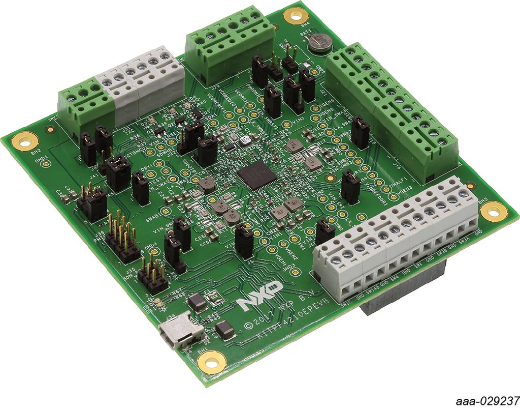
1 1 KITPF410EPEVB
2 Important notice NXP provides the enclosed product(s) under the following conditions: This evaluation kit is intended for use of ENGINEERING DEVELOPMENT OR EVALUATION PURPOSES ONLY. It is provided as a sample IC pre-soldered to a printed circuit board to make it easier to access inputs, outputs, and supply terminals. This evaluation board may be used with any development system or other source of I/O signals by simply connecting it to the host MCU or computer board via off-theshelf cables. This evaluation board is not a Reference Design and is not intended to represent a final design recommendation for any particular application. Final device in an application will be heavily dependent on proper printed circuit board layout and heat sinking design as well as attention to supply filtering, transient suppression, and I/O signal quality. The goods provided may not be complete in terms of required design, marketing, and or manufacturing related protective considerations, including product safety measures typically found in the end product incorporating the goods. Due to the open construction of the product, it is the user's responsibility to take any and all appropriate precautions with regard to electrostatic discharge. In order to minimize risks associated with the customers applications, adequate design and operating safeguards must be provided by the customer to minimize inherent or procedural hazards. For any safety concerns, contact NXP sales and technical support services. Should this evaluation kit not meet the specifications indicated in the kit, it may be returned within 30 days from the date of delivery and will be replaced by a new kit. NXP reserves the right to make changes without further notice to any products herein. NXP makes no warranty, representation or guarantee regarding the suitability of its products for any particular purpose, nor does NXP assume any liability arising out of the application or use of any product or circuit, and specifically disclaims any and all liability, including without limitation consequential or incidental damages. Typical parameters can and do vary in different applications and actual performance may vary over time. All operating parameters, including Typical, must be validated for each customer application by customer s technical experts. NXP does not convey any license under its patent rights nor the rights of others. NXP products are not designed, intended, or authorized for use as components in systems intended for surgical implant into the body, or other applications intended to support or sustain life, or for any other application in which the failure of the NXP product could create a situation where personal injury or death may occur. Should the Buyer purchase or use NXP products for any such unintended or unauthorized application, the Buyer shall indemnify and hold NXP and its officers, employees, subsidiaries, affiliates, and distributors harmless against all claims, costs, damages, and expenses, and reasonable attorney fees arising out of, directly or indirectly, any claim of personal injury or death associated with such unintended or unauthorized use, even if such claim alleges NXP was negligent regarding the design or manufacture of the part. NXP and the NXP logo are trademarks of NXP B.V. All other product or service names are the property of their respective owners. NXP B.V / 18
3 3 Getting started The NXP analog product development boards provide an easy-to-use platform for evaluating NXP products. The boards support a range of analog, mixed-signal and power solutions. They incorporate monolithic integrated circuits and system-in-package devices that use proven high-volume technology. NXP products offer longer battery life, a smaller form factor, reduced component counts, lower cost and improved performance in powering state-of-the-art systems. The tool summary page for KITPF410EPEVB is located at KITPF410EPEVB. The overview tab provides an overview of the device, product features, a description of the kit contents, a list of (and links to) supported devices, list of (and links to) any related products and a Get Started section. The Get Started section provides links to everything needed to start using the device and contains the most relevant, current information applicable to the KITPF410EPEVB. Go to On the Overview tab, locate the Jump To navigation feature on the left side of the window. Select either the Get Started link or scroll in the main window of the Overview tab until the Get Started section is visible. Review each entry in the Get Started section. Download an entry by clicking on the title. After reviewing the Overview tab, visit the other product related tabs for additional information: Documentation: download current documentation Software & Tools: download current hardware and software tools Buy/Parametrics: purchase the product and view the product parametrics After downloading files, review each file, including the user guide which includes setup instructions. If applicable, the bill of materials (BOM) and supporting schematics are also available for download in the Get Started section of the Overview tab. 3.1 Kit contents/packing list The KITPF410EPEVB contents include: Assembled and tested KITPF410EPEVB board in an anti-static bag Quick start guide Warranty card 3. Required equipment To use this kit, you need: Power supply: Output voltage range from 3.1 V to 4.5 V Current capability from 3.0 to 5.0 A (current requirement is dependent on output loading) Supply to board connection cables (capable of withstanding up to 5.0 A current) USB (male) to mini USB (male) communication cable USB-enabled computer 3 / 18
4 3.3 System requirements The kit requires the following to function properly with the software: Windows XP or Windows 7 operating system 4 Getting to know the hardware 4.1 Board features Input voltage operation range from 3.1 V to 4.5 V Output voltage supplies accessible through detachable terminal blocks Four to six independent buck converters One 5.0 V boost regulator Six general purpose LDO regulators One DDR memory termination voltage reference One VSRTC supply Coin cell support for Try-Before-Buy (TBB) mode On/off push button support Hardware configuration flexibility through various jumper headers and resistors Integrated USB to I C programming interface for full control/configuration Onboard PMIC control through the I C register map Fully featured programmer through J36 for external device control/programming On board connectors for interfacing with future evaluation/debug tools Compact form factor (4 x 4 in ) 4 / 18
5 4. Device features Table 1. Device features Device Description Features PF410 The PF410 Power Management Integrated Circuit (PMIC) provides a highly programmable/configurable architecture with fully integrated power devices and minimal external components. With up to six buck converters, six linear regulators, RTC supply, and coin-cell charger, the PF410 can provide power for a complete system, including applications processors, memory, and system peripherals, in a wide range of applications. Four to six buck converters, depending on configuration Single/Dual phase/ parallel options DDR termination tracking mode option Boost regulator to 5.0 V output Six general purpose linear regulators Programmable output voltage, sequence, and timing OTP (One Time Programmable) memory for device configuration Coin cell charger and RTC supply DDR termination reference voltage Power control logic with processor interface and event detection I C control Individually programmable ON, OFF, and Standby modes MC9S08JM60 The KITPF410EPEVB implements a NXP MC9S08JM60 low-cost, high-performance 8-bit HCS08 microcontroller to interface via USB to I C to control the main PMIC. 8-bit HCS08 Central Processing Unit (CPU) Up to 4 MHz internal bus (48 MHz HCS08 core) frequency offering.7 to 5.5 V across temperature range of 40 C to +85 C Support for up to 3 peripheral interrupt/reset sources On-chip memory Up to 60 K flash read/program/erase over full operating voltage and temperature Up to 4 K RAM 56 Byte USB RAM 4.3 Board description The KITPF410EPEVB operates with a single power supply from 3.1 V to 4.5 V and is controlled via USB with help of an integrated USB-IC communication bridge. By applying the input voltage supply, the KITPF410EPEVB powers up according to the default power-up sequence described in the PF410 data sheet. Important: If power-up sequences and configurations are to be modified, the user must ensure that the register settings are consistent with the hardware configuration. This is most important for the buck regulators, where the quantity, size, and value of the inductors depend on the configuration (single/dual phase or independent mode) and the switching frequency. Additionally, if an LDO is powered by a buck regulator, it is gated by the buck regulator in the start-up sequence. See PF410 data sheet for details on buck regulator setup Jumper definitions By default, the is set to power up from the default power-up sequence. Verify that the jumpers are placed in the right position as shown in Figure 1. For a detailed description of the jumper functionality, see Table. 5 / 18

6 Figure 1. Default jumper configuration Table. Jumper definitions Jumper Default Description J1-J7 Buck regulators input power path isolation Short these jumpers to allow SWxIN to be powered from the SWVIN supply J9 SWBST regulator input power path isolation Short this jumper to allow SWBSTIN to be powered from the SWVIN supply J VDDOTP supply selector 1-: Connect VDDOTP to the OTP Boost output (VDDOTPIN) for OTP programming 3-4: Connect VDDOTP to GND to power up from OTP/TBB sequence 5-6: Connect VDDOTP to VCOREDIG to power up from default power-up sequence J0 1- Coin cell selector 1-: Enables BAT1 as the main coin cell supply -3: Enables BAT as the main coin cell supply J40 Shorts PVIN and SWVIN Allows supply isolation to provide more accurate efficiency readings on the switching supplies J41 Open Shorts SWVIN to VIN Allows one to isolate or connect the PF410 logic input supply to SWVIN net. (debugging option) J7 Shorts PVIN to VIN Allows one to isolate or connect the PF410 logic input supply to PVIN net. (debugging option) J -3 PF410 input logic supply selector 1-: Connects PF410 VIN terminal to the 3.3 V external LDO regulator for debugging purposes -3: Connects PF40 VIN terminal to the main input supply J6 Open Short to hold PWRON pin low J4 Open Short to pull STANDBY to VSNVS voltage supply J39 1- Control interface input supply selector 1-: Enables PVIN node as the input supply source for the control interface -3: Enables USB power as the input supply source for the control interface 6 / 18
7 4.3. Connector and terminal block definitions Table 3. Terminal block definitions Connector Function Pin definition J8 SWBST Pin 1 - SWBST output J10 SW1AB Pin 1 - SW1AB output J11 SW1C Pin 1 - SW1C output J1 SW Pin 1 - SW output J13 SW4 Pin 1 - SW4 output J14 SW3A Pin 1 - SW3A output J15 SW3B Pin 1 - SW3B output J16 VGEN1/VGEN Pin 1 - VGEN1 output Pin 3 - VGEN output J18 VGEN3/VGEN4 Pin 1 - VGEN3 output Pin 3 - VGEN4 output J19 VGEN5/VGEN6 Pin 1 - VGEN5 output Pin 3 - VGEN6 output J1 VSNVS/VREFDDR Pin 1 - VSNVS output Pin 3 - VREFDDR output J5 Main input supply Pin 1 - GND Pin - PVIN Pin 3 - SWVIN J9 Interfacing 1 Pin 1 - INTB Pin - SDWNB Pin 3 - RESETBMCU J3 Interfacing Pin 1 - STANDBY Pin - PWRON Pin 3 - GND J31 I C signals Pin 1 - SCL Pin - SDA J33 VDDIO Pin 1 - VDDIO 7 / 18

8 Figure. Input/output terminal blocks Table 4. Connector definitions Connector Function Pin definition J34 Mini USB connector Pin 1 - VBUS Pin - D Pin 3 - D+ Pin 4 - NC Pin 5 - GND Chassis - GND J35 BDM connector Pin 1 - BKGD_JM60 Pin 3 - NC Pin 4 - RST_JM60 Pin 5 - NC Pin 6 - USB_PWR J36 Programmer connector Pin 1 - VDDOTPIN (8.5 V boost output) Pin - 3V3 (3.3 V LDO output) Pin 3 - GND Pin 4 - MCU_SCL (I C clock signal) Pin 5 - MCU_SDA (I C data signal) Pin 6 - PWRON (controls the PWRON on the target device) Pin 7 - GPIO 1 (general purpose GPIO) Pin 8 - GPIO (general purpose GPIO) J4 Debug Port 1 Debugging connector for future development tools J43 Debug Port Debugging connector for future development tools J44 Debug Port 3 Debugging connector for future development tools 8 / 18
9 4.3.3 Debug and configuration components The KITPF410EPEVB allows full flexibility to change the default configuration of SW1A/ B/C and SW3A/B outputs to one more suitable for a specific application scenario. It also provides several source options for the LDO supplies to test various loading and supplying scenarios. Test points are provided on key nodes of the KITPF410EPEVB to allow full debugging capability during application development SW1A/B/C configuration components The SW1A/B/C regulator can be configured in various operating modes as described in Table 5. Figure 3. SW1A/B/C output configuration Table 5. SW1A/B/C configuration chart Component SW1A/B/C single phase SW1A/B single phase SW1C independent SW1A/B dual phase SW1C independent R6 R9 R4 R7 R8 R10 R11 L ISAT = 6.0 A ISAT = 4.5 A ISAT =.4 A L3 N/A N/A ISAT =.4 A L4 N/A ISAT =.4 A ISAT =.4 A SW3A/B configuration components The SW3A/B regulator can be configured in various operating modes as described in Table 6. 9 / 18
10 Figure 4. SW3A/B output configuration Table 6. SW3A/B configuration chart Component SW3A/B single phase SW3A/B dual phase SW3A independent SW3B independent R16 R17 R70 L7 ISAT = 3.9 A ISAT = 3.0 A ISAT = 3.0 A L8 N/A ISAT = 3.0 A ISAT = 3.0 A LDO input supply source selection Figure 5. LDO schematic configuration Figure 6. Logic and core supplies 10 / 18

11 Table 7. LDO input supply configuration chart [1] Input pin Input options VIN1 Input supply for VGEN1 and VGEN R0 = SW4 R1 = SW VIN Input supply for VGEN3 and VGEN4 R4 = SW4 R = SW VIN3 Input supply for VGEN5 and VGEN6 R3 = VIN R5 = SW VINREFDDR VREFDDR input supply R6 = SW3A R7 = SW3B VDDIO VDDIO input supply 3V3 J46 = 1- SW J46 = -3 [1] Make sure to populate only one option per input pin to avoid shorts between various sources Test point definitions All test points are clearly marked on the. Figure 7 shows the location of various test points. Figure 7. Key test point locations and default voltages Miscellaneous components Power on push button A footprint for a normally open, momentary push-button is provided at the PWRON terminal to allow a momentary low state by pressing the push button. J47 allows isolation of the PWRON terminal from the MCU GPIO controlling this pin. 11 / 18
12 Figure 8. Power on circuit PMIC LED indicators LED indicators are provided to notify the PMIC status to the user. Figure 9 shows the PMIC status. LEDs D and D4, and a reserved LED indicator D3, allow an external rework connection to the transistor gate if any given signal debug is required. Figure 9. PMIC status indicator Table 8. LED state description LED Description D Interrupt notification ON = PMIC has detected an unmasked interrupt OFF = No interrupt detected D4 RESETBMCU notification Green = PMIC is in regulation and operating properly Red = PMIC is out of regulation D3 PWRON notification ON = PWRON is low OFF = PWRON is high 1 / 18
13 Control/programming interface This onboard USB-to-I C interface comprises three basic blocks. 1. Controlling MCU (MC9S08JM60CGTE) for USB-IC translation. 3.3 V LDO supply for external device controlling V boost converter for OTP programming The control/programming interface allows one to program the onboard PF410 PMIC. Alternatively, the interface can serve as a programmer for external devices though the connector J36. Figure 10. Control/programming interface 5 Configuring the hardware Connect the power supply and the USB communication cables as shown in Figure 11. Voltmeters are optional but it is recommended in order to accurately verify that each one of the output supplies is providing the correct voltage level. 13 / 18
. If the SW regulator is to be set below 3.0 V, then switch the 3.3 V LDO connection to VDDIO (J46 = 1-).")
14 Figure 11. Evaluation board setup Note: The KITPF410EPEVB allows the selection of SW regulator output or an external 3.3 V LDO output as the VDDIO/I C pull-up supply. By default, the SW regulator is the source for the VDDIO supply (J46 = 3-4). If the SW regulator is to be set below 3.0 V, then switch the 3.3 V LDO connection to VDDIO (J46 = 1-). 6 Schematics, board layout and bill of materials Board schematics, board layout and bill of materials are available in the download tab of the tool summary page: 14 / 18
15 7 References Following are URLs where you can obtain information on related NXP products and application solutions: NXP.com support pages Description URL KITPF410EPEVB Tool summary page PF410 Product summary page Revision history Revision history Rev Date Description v Initial version 15 / 18
16 8 Legal information 8.1 Definitions Draft The document is a draft version only. The content is still under internal review and subject to formal approval, which may result in modifications or additions. does not give any representations or warranties as to the accuracy or completeness of information included herein and shall have no liability for the consequences of use of such information. 8. Disclaimers Limited warranty and liability Information in this document is believed to be accurate and reliable. However, does not give any representations or warranties, expressed or implied, as to the accuracy or completeness of such information and shall have no liability for the consequences of use of such information. takes no responsibility for the content in this document if provided by an information source outside of. In no event shall NXP Semiconductors be liable for any indirect, incidental, punitive, special or consequential damages (including - without limitation - lost profits, lost savings, business interruption, costs related to the removal or replacement of any products or rework charges) whether or not such damages are based on tort (including negligence), warranty, breach of contract or any other legal theory. Notwithstanding any damages that customer might incur for any reason whatsoever, aggregate and cumulative liability towards customer for the products described herein shall be limited in accordance with the Terms and conditions of commercial sale of NXP Semiconductors. Right to make changes reserves the right to make changes to information published in this document, including without limitation specifications and product descriptions, at any time and without notice. This document supersedes and replaces all information supplied prior to the publication hereof. Suitability for use products are not designed, authorized or warranted to be suitable for use in life support, life-critical or safety-critical systems or equipment, nor in applications where failure or malfunction of an product can reasonably be expected to result in personal injury, death or severe property or environmental damage. and its suppliers accept no liability for inclusion and/or use of products in such equipment or applications and therefore such inclusion and/or use is at the customer s own risk. Applications Applications that are described herein for any of these products are for illustrative purposes only. makes no representation or warranty that such applications will be suitable for the specified use without further testing or modification. Customers are responsible for the design and operation of their applications and products using products, and accepts no liability for any assistance with applications or customer product design. It is customer s sole responsibility to determine whether the NXP Semiconductors product is suitable and fit for the customer s applications and products planned, as well as for the planned application and use of customer s third party customer(s). Customers should provide appropriate design and operating safeguards to minimize the risks associated with their applications and products. does not accept any liability related to any default, damage, costs or problem which is based on any weakness or default in the customer s applications or products, or the application or use by customer s third party customer(s). Customer is responsible for doing all necessary testing for the customer s applications and products using products in order to avoid a default of the applications and the products or of the application or use by customer s third party customer(s). NXP does not accept any liability in this respect. Export control This document as well as the item(s) described herein may be subject to export control regulations. Export might require a prior authorization from competent authorities. Non-automotive qualified products Unless this data sheet expressly states that this specific product is automotive qualified, the product is not suitable for automotive use. It is neither qualified nor tested in accordance with automotive testing or application requirements. accepts no liability for inclusion and/or use of nonautomotive qualified products in automotive equipment or applications. In the event that customer uses the product for design-in and use in automotive applications to automotive specifications and standards, customer (a) shall use the product without warranty of the product for such automotive applications, use and specifications, and (b) whenever customer uses the product for automotive applications beyond NXP Semiconductors specifications such use shall be solely at customer s own risk, and (c) customer fully indemnifies for any liability, damages or failed product claims resulting from customer design and use of the product for automotive applications beyond standard warranty and product specifications. Evaluation products This product is provided on an as is and with all faults basis for evaluation purposes only., its affiliates and their suppliers expressly disclaim all warranties, whether express, implied or statutory, including but not limited to the implied warranties of non-infringement, merchantability and fitness for a particular purpose. The entire risk as to the quality, or arising out of the use or performance, of this product remains with customer. In no event shall, its affiliates or their suppliers be liable to customer for any special, indirect, consequential, punitive or incidental damages (including without limitation damages for loss of business, business interruption, loss of use, loss of data or information, and the like) arising out the use of or inability to use the product, whether or not based on tort (including negligence), strict liability, breach of contract, breach of warranty or any other theory, even if advised of the possibility of such damages. Notwithstanding any damages that customer might incur for any reason whatsoever (including without limitation, all damages referenced above and all direct or general damages), the entire liability of, its affiliates and their suppliers and customer s exclusive remedy for all of the foregoing shall be limited to actual damages incurred by customer based on reasonable reliance up to the greater of the amount actually paid by customer for the product or five dollars (US$5.00). The foregoing limitations, exclusions and disclaimers shall apply to the maximum extent permitted by applicable law, even if any remedy fails of its essential purpose. Translations A non-english (translated) version of a document is for reference only. The English version shall prevail in case of any discrepancy between the translated and English versions. 8.3 Trademarks Notice: All referenced brands, product names, service names and trademarks are the property of their respective owners. 16 / 18
17 Tables Tab. 1. Tab.. Tab. 3. Tab. 4. Device features... 5 Jumper definitions... 6 Terminal block definitions...7 Connector definitions...8 Tab. 5. Tab. 6. Tab. 7. Tab. 8. SW1A/B/C configuration chart...9 SW3A/B configuration chart LDO input supply configuration chart LED state description... 1 Fig. 7. Fig. 8. Fig. 9. Fig. 10. Fig. 11. Key test point locations and default voltages Power on circuit... 1 PMIC status indicator... 1 Control/programming interface Evaluation board setup Figures Fig. 1. Fig.. Fig. 3. Fig. 4. Fig. 5. Fig. 6. Default jumper configuration... 6 Input/output terminal blocks... 8 SW1A/B/C output configuration...9 SW3A/B output configuration LDO schematic configuration Logic and core supplies / 18
18 Contents KITPF410EPEVB...1 Important notice... Getting started... 3 Kit contents/packing list... 3 Required equipment... 3 System requirements...4 Getting to know the hardware... 4 Board features... 4 Device features...5 Board description...5 Jumper definitions... 5 Connector and terminal block definitions... 7 Debug and configuration components... 9 SW1A/B/C configuration components...9 SW3A/B configuration components... 9 LDO input supply source selection Test point definitions...11 Miscellaneous components Power on push button PMIC LED indicators... 1 Control/programming interface Configuring the hardware Schematics, board layout and bill of materials...14 References Legal information Please be aware that important notices concerning this document and the product(s) described herein, have been included in section 'Legal information'. NXP B.V All rights reserved. For more information, please visit: For sales office addresses, please send an to: salesaddresses@nxp.com Date of release: 8 February 018
UM NVT2001GM and NVT2002DP demo boards. Document information
 Rev. 7 March 202 User manual Document information Info Keywords Abstract Content NVT, voltage translator, level translator, level shift, passive voltage translator, passive level translator, passive level
UM NVT2008PW and NVT2010PW demo boards. Document information
 Rev. 1 March 20 User manual Document information Info Keywords Abstract Content NVT, voltage translator, level translator, level shift, passive voltage translator, passive level translator, passive level
UM NXP USB PD shield board user manual COMPANY PUBLIC. Document information
 Rev. 0.3 19 June 2017 User manual COMPANY PUBLIC Document information Information Content Keywords Abstract OM13588, USB Type-C, PD (power delivery), Alt-mode-DP, Host, Dock This user manual presents demonstration
UM PCAL6524 demonstration board OM Document information
 Rev. 1 23 September 2015 User manual Document information Info Content Keywords OM13320 Fm+ development kit, OM13260 Fm+ I2C bus development board, OM13303 GPIO target board Abstract Installation guide
KITPF0100SKTEVBE Programming Socket
 Freescale Semiconductor, Inc. User s Guide Document Number: KTPFSKTUG Rev.., 6/3 KITPFSKTEVBE Programming Socket Configures PF Family Devices Figure. PF Programming Socket (KITPFSKTEVBE) Table of Contents
OM bit GPIO Daughter Card User Manual
 OM13489 16-bit GPIO Daughter Card User Manual Rev. 2.0 09 January 2014 User manual Document information Info Content Keywords Fm+ Development Kit, OM13320, GPIO, OM13303 Abstract Installation guide and
How to use the NTAG I²C plus for bidirectional communication. Rev June
 How to use the NTAG I²C plus for bidirectional communication Document information Info Content Keywords NTAG I 2 C plus, pass-through mode, bidirectional communication, SRAM Abstract This document describes
UM PR533 - PCSC Tool. User manual COMPANY PUBLIC. Rev November Document information
 PR533 - PCSC Tool Document information Info Content Keywords PR533, CCID, PCSC, APDU Abstract This document describes the PCSC Tool software which demonstrates the capabilities of PR533 device. Revision
AN NTAG I²C plus memory configuration options. Application note COMPANY PUBLIC. Rev June Document information
 Document information Info Content Keywords NTAG I²C plus, memory configuration, NDEF, read-only, EEPROM Abstract Describe how to configure the NTAG I²C plus in the different use case for read/write, read-only
QPP Proprietary Profile Guide
 Rev. 04 April 2018 Application note Document information Info Content Keywords Proprietary Profile, Server, Client Abstract The Proprietary Profile is used to transfer the raw data between BLE devices.
UM NXP USB Type-C Shield 2 Demo Kit User Manual COMPANY PUBLIC. Document information
 Document information Information Content Keywords USB Type-C, PD (power delivery), Alt-mode-DP, Host, Dock, Shield, PTN5110, PTN5110N Abstract This user manual presents demonstration / application kit
UM OM bit GPIO Daughter Card User Manual. Document information. Keywords Abstract
 OM13488 8-bit GPIO Daughter Card User Manual Rev. 1.0 11 October 2013 User manual Document information Info Keywords Abstract Content Fm+ Development Kit, OM13320, GPIO, OM13303 Installation guide and
KIT34901EFEVB Evaluation Board
 Freescale Semiconductor, Inc. User s Guide Document Number: KT34901UG Rev. 1.0, 2/2014 KIT34901EFEVB Evaluation Board Featuring the MC34901 High Speed CAN Transceiver Contents Figure 1. KIT34901EFEVB Evaluation
UM10766 User manual for the I2C-bus RTC PCF85263A demo board OM13510
 User manual for the I2C-bus RTC PCF85263A demo board OM13510 Rev. 1 15 November 2013 User manual Document information Info Content Keywords PCF85263, OM13510, demo board, how to get started, I 2 C-bus,
AN BGA301x Wideband Variable Gain Amplifier Application. Document information. Keywords
 Rev. 2 3 February 2014 Application note Document information Info Content Keywords BGA3015, BGA3018, BAP70Q, CATV, Line-up, VGA, Evaluation board Abstract This application note describes the schematic
UM LPC General Purpose Shield (OM13082) Rev November Document information. Keywords
 Rev November Document information. Keywords") Rev. 1.0 17 November 2015 User manual Document information Info Content Keywords LPCXpresso, LPC General Purpose Shield, OM13082 Abstract LPC General Purpose Shield User Manual Revision history Rev Date
Rev. 1.0 17 November 2015 User manual Document information Info Content Keywords LPCXpresso, LPC General Purpose Shield, OM13082 Abstract LPC General Purpose Shield User Manual Revision history Rev Date
AN BGA GHz 18 db gain wideband amplifier MMIC. Document information. Keywords. BGA3018, Evaluation board, CATV, Drop amplifier.
 Rev. 2 8 January 2013 Application note Document information Info Keywords Abstract Content BGA3018, Evaluation board, CATV, Drop amplifier This application note describes the schematic and layout requirements
AN CBTL08GP053 Programmer's Guide. Document information. Keywords Abstract
 Rev. 1 18 June 2015 Application note Document information Info Content Keywords Abstract USB Type-C, multiplexer, switch, USB 3.1, DP 1.3, DP++, PCIe 3.0, I 2 C This document describes the application
KIT33972AEWEVBE Evaluation Board
 Freescale Semiconductor, Inc. User s Guide Document Number: KT33972UG Rev. 1.0, 7/2013 KIT33972AEWEVBE Evaluation Board Featuring the MC33972A Multiple Switch Detection Interface IC Contents Figure 1.
UM EEPROM Management of PN746X and PN736X. User manual COMPANY PUBLIC. Rev February Document information
 Document information Info Content Keywords Abstract PN7462, PN7362, PN7360; EEPROM This document describes how to manage EEPROM of PN7462 family. Revision history Rev Date Description 1.0 20170202 First
AN LPC82x Touch Solution Quick Start Guide. Document information. Keywords
 Rev. 1.0 22 December 2014 Application Note Document information Info Keywords Abstract Content Capacitive Touch, Touchpad, Sensor, Electrode, Drive/Sensing lines, Dielectric, Overlay panel, Sensitivity,
UM User manual for the BGU MHz LNA evaluation board. Document information
 User manual for the BGU7003 868MHz LNA evaluation board Rev.1.0 06 December 2011 User manual Document information Info Content Keywords 868MHz LNA, BGU7003. Application Board ordering info: Abstract This
Broadband system applications i.e. WCDMA, CATV, etc. General purpose Voltage Controlled Attenuators for high linearity applications
 Rev. 2 6 March 2012 Product data sheet 1. Product profile 1.1 General description Quad PIN diode in a SOT753 package. 1.2 Features and benefits 4 PIN diodes in a SOT753 package 300 khz to 4 GHz High linearity
Using LPC11Axx EEPROM (with IAP)
") Rev. 2 1 July 2012 Application note Document information Info Content Keywords LPC11A02UK ; LPC11A04UK; LPC11A11FHN33; LPC11A12FHN33; LPC11A12FBD48; LPC11A13FHI33; LPC11A14FHN33; LPC11A14FBD48; LPC11Axx,
Rev. 2 1 July 2012 Application note Document information Info Content Keywords LPC11A02UK ; LPC11A04UK; LPC11A11FHN33; LPC11A12FHN33; LPC11A12FBD48; LPC11A13FHI33; LPC11A14FHN33; LPC11A14FBD48; LPC11Axx,
CAUTION This device is sensitive to ElectroStatic Discharge (ESD). Therefore care should be taken during transport and handling.
. Therefore care should be taken during transport and handling.") Rev. 2 28 September 2010 Product data sheet 1. Product profile 1.1 General description Hybrid high dynamic range amplifier module operating at a supply voltage of 24 V (DC) in an SOT115J package. The module
Rev. 2 28 September 2010 Product data sheet 1. Product profile 1.1 General description Hybrid high dynamic range amplifier module operating at a supply voltage of 24 V (DC) in an SOT115J package. The module
IoT Sensing SDK. Getting started with IoT Sensing SDK (ISSDK) v1.7 middleware. Document information. IoT Sensing SDK, ISSDK, MCUXpresso, middleware
 v1.7 middleware. Document information. IoT Sensing SDK, ISSDK, MCUXpresso, middleware") Getting started with (ISSDK) v1.7 middleware Document information Information Content Keywords, ISSDK, MCUXpresso, middleware Abstract 1 Prerequisites This document assumes completion of the following
Getting started with (ISSDK) v1.7 middleware Document information Information Content Keywords, ISSDK, MCUXpresso, middleware Abstract 1 Prerequisites This document assumes completion of the following
UM Gaming suitcase demo system. Document information
 Rev. 1 9 August 2012 User manual Document information Info Keywords Abstract Content I2C-bus, I2C, PCU9669, bus controllers, LED driver, stepper motor, Fast-mode Plus, Fm+, Ultra Fast-mode, UFm The Gaming
AN10942 MFRX852 Evaluation Board- Quick start up Guide
 MFRX852 Evaluation Board- Quick start up Guide Document information Info Content Keywords MIFARE SAM AV1, RC523, MFRX852, misam-x, MFRX623. Abstract This application note provides the guidance of using
STB-CE v Overview. 2 Features. Release notes for STB-CE v What's new in STB-CE v2.5
 Rev. 3 10 May 2018 Release notes 1 Overview The Freedom Sensor Toolbox-Community Edition (STB-CE) is the visualization and evaluation software in the Sensor Toolbox ecosystem. It enables quick and easy
PNP 500 ma, 50 V resistor-equipped transistor; R1 = 2.2 kω, R2 = open
 PNP 500 ma, 50 V resistor-equipped transistor; R1 = 2.2 kω, R2 = open Rev. 4 8 November 2010 Product data sheet 1. Product profile 1.1 General description 500 ma PNP Resistor-Equipped Transistor (RET)
UM OM11057 quick start guide. Document information
 Rev. 2 10 April 2013 User manual Document information Info Keywords Abstract Content Capacitive switch, sensor, proximity switch, OM11057, PCF8885, PCA8885, PCA8886, evaluation board The OM11057 is an
AN Over-the-Air top-up with MIFARE DESFire EV2 and MIFARE Plus EV1. Document information
 Over-the-Air top-up with MIFARE DESFire EV2 and MIFARE Plus EV1 Document information Information Content Keywords Over-the-Air, OTA, Top-up, MIFARE DESFire EV2, MIFARE Plus EV1, Stored Value, Transport
NWP2081T. 1. General description. 2. Features and benefits. 3. Applications. 4. Ordering information. Half-bridge driver IC
 Rev. 1 3 September 2013 Product data sheet 1. General description The is a high-voltage monolithic integrated circuit made using the latch-up free Silicon-On-Insulator (SOI) process. The circuit is designed
SiGe:C Low Noise High Linearity Amplifier
 Rev. 2 21 February 212 Product data sheet 1. Product profile 1.1 General description The is a low noise high linearity amplifier for wireless infrastructure applications.the LNA has a high input and output
AN10955 Full-duplex software UART for LPC111x and LPC13xx
 Rev. 1 13 July 2010 Application note Document information Info Content Keywords LPC111X, LPC13XX, UART, software Abstract This application note illustrates how software running on an LPC111X or LPC13XX
PESD18VV1BBSF. Very symmetrical bidirectional ESD protection diode
 Rev. 1 2 December 217 Product data sheet 1 Product profile 1.1 General description Very symmetrical bidirectional ElectroStatic Discharge (ESD) protection diode. This device is housed in a DSN63-2 (SOD962)
Bidirectional ESD protection diode
 11 December 2018 Preliminary data sheet 1. General description 2. Features and benefits 3. Applications 4. Quick reference data Ultra low capacitance bidirectional ElectroStatic Discharge (ESD) protection
74ABT General description. 2. Features and benefits. 3. Ordering information. Quad 2-input AND gate
 Rev. 3 20 November 2015 Product data sheet 1. General description The high-performance BiCMOS device combines low static and dynamic power dissipation with high speed and high output drive. The is a quad
NXP AN11528 sensor Application note
 NXP sensor Application note http://www.manuallib.com/nxp/an11528-sensor-application-note.html This application note will illustrate the new features of the LPC11U6x device family compared to the LPC11U3x
KIT33887EKEVB Evaluation Board
 Freescale Semiconductor, Inc User s Guide Document Number: KT33887UG Rev 20, 4/2013 KIT33887EKEVB Evaluation Board Featuring the MC33887EK 50 A H-Bridge IC Contents Figure 1 KIT33887EKEVB Evaluation Board
KTTWRCM3120UG TWR-CM3120-EVM. TWR-CM3120-EVM Tower System Platform. Figure 1. TWR-CM3120-EVM
 TWR-CM0-EVM Figure. TWR-CM0-EVM Important notice NXP provides the enclosed product(s) under the following conditions: This evaluation kit is intended for use of ENGINEERING DEVELOPMENT OR EVALUATION PURPOSES
PESD24VF1BSF. Table 1. Quick reference data Symbol Parameter Conditions Min Typ Max Unit C d diode capacitance f = 1 MHz; V R = 0 V
 11 December 2015 Product data sheet 1. General description Ultra low capacitance bidirectional ElectroStatic Discharge (ESD) protection diode in a DSN0603-2 (SOD962-2) leadless ultra small Surface-Mounted
PESD5V0C1USF. in portable electronics, communication, consumer and computing devices.
 6 May 215 Product data sheet 1. General description Ultra low capacitance unirectional ElectroStatic Discharge (ESD) protection diode, part of the TrEOS Protection family. This device is housed in a DSN63-2
PESD18VF1BL. 1. General description. 2. Features and benefits. 3. Applications. 4. Quick reference data. 5. Pinning information
 10 July 2018 Product data sheet 1. General description Ultra low capacitance bidirectional ElectroStatic Discharge (ESD) protection diode in a DFN1006-2 (SOD882) leadless ultra small Surface-Mounted Device
NCR402T. 1. General description. 2. Features and benefits. 3. Applications. 4. Quick reference data
 16 October 2015 Product data sheet 1. General description LED driver consisting of a resistor-equipped PNP transistor with two diodes on one chip in a small SOT23 plastic package. 2. Features and benefits
AN MIFARE Type Identification Procedure. Application note COMPANY PUBLIC. Rev August Document information
 Document information Info Content Keywords, 14443 Abstract This document describes how to differentiate between the members of the card IC family. 14443-3 describes the initialization and anti-collision
OM13071 LPCXpresso824-MAX Development board
 LPCXpresso824-MAX Development board Rev. 1 29 September 2014 User manual Document information Info Content Keywords, LPC82x, development board, mbed, arduino Abstract This user manual describes the LPCXpresso824-MAX
In data sheets and application notes which still contain NXP or Philips Semiconductors references, use the references to Nexperia, as shown below.
 Important notice Dear Customer, On 7 February 2017 the former NXP Standard Product business became a new company with the tradename Nexperia. Nexperia is an industry leading supplier of Discrete, Logic
AN12119 A71CH Quick start guide for OM3710A71CHARD and i.mx6ultralite
 A71CH Quick start guide for OM3710A71CHARD and i.mx6ultralite Document information Info Keywords Abstract Content Security IC, i.mx6ultralite, OM3710A71CHARD, MCIMX6UL-EVKB This document provides a detailed
LPC-Link2 Debug Probe Firmware Programming. Rev June, 2017 User Guide
 LPC-Link2 Debug Probe Firmware Programming 19 June, 2017 Copyright 2015 NXP Semiconductors All rights reserved. - ii 1. Revision History... 1 1.1. v1.8.2... 1 1.2. v1.5.2... 1 1.3. v1.5... 1 2. Introduction...
UM OM13500 & OM13500A, PCA9620 & PCx8537 demo board. Document information. Keywords
 OM13500 & OM13500A, PCA9620 & PCx8537 demo board Rev. 1 23.September 2013 User manual Document information Info Content Keywords LCD, Liquid Crystal Display, LCD driver, segment driver, PCA9620, PCF8537,
MMBZ16VAL. 1. General description. 2. Features and benefits. 3. Applications. 4. Quick reference data
 High surge current unidirectional double ESD protection diodes 6 November 217 Product data sheet 1. General description Unidirectional double ElectroStatic Discharge (ESD) protection diodes in a common
300 V, 100 ma PNP high-voltage transistor
 SOT89 Rev. 6 27 September 2011 Product data sheet 1. Product profile 1.1 General description PNP high-voltage transistor in a medium power and flat lead SOT89 (SC-62) Surface-Mounted Device (SMD) plastic
UM NTAG I²C plus Explorer Kit Peek and Poke. Rev September User manual COMPANY PUBLIC. Document information
 360221 Document information Info Content Keywords NTAG I 2 C plus, Explorer Kit, PC, NFC Tag, Peek and Poke Abstract This User Manual aims at describing the functionalities and how to use the Peek and
UM LPC54114 Audio and Voice Recognition Kit. Rev February Document information. Keywords
 Rev. 1.1 25 February 2016 User manual Document information Info Content Keywords LPCXpresso54114, LPC54110, LPC5411x, Voice Abstract LPC54114 audio and voice recognition kit User Manual Revision history
QN908x. DK User s Guide. Document information. QN9080-DK, QN9080, QN9083, BLE, USB Dongle This document is an introduction to the QN908x DK V1.
 Rev. 1.2 April 2018 Info Keywords Abstract Document information Content QN9080-DK, QN9080, QN9083, BLE, USB Dongle This document is an introduction to the DK V1.2 board Rev Date Description 0.1 20160818
ESD protection for ultra high-speed interfaces
 XSON7 Rev. 1 19 August 214 Product data sheet 1. Product profile 1.1 General description The device is designed to protect high-speed interfaces such as SuperSpeed and Hi - Speed USB combination, Secure
PESD5V0X2UM. 1. General description. 2. Features and benefits. 3. Applications. 4. Quick reference data
 Ultra low capacitance unidirectional double ESD protection diode 3 February 2014 Product data sheet 1. General description Ultra low capacitance unidirectional double ElectroStatic Discharge (ESD) protection
UM LPCXpresso Rev th November Document information. LPCXpresso54102, LPC54100 LPCXpresso54102 User Manual
 LPCXpresso54102 Rev. 1.0 4th November 2014 User manual Document information Info Content Keywords LPCXpresso54102, LPC54100 Abstract LPCXpresso54102 User Manual Revision history Rev Date Description 1.0
KIT33988CEVBE evaluation board
 NXP Semiconductors User s Guide Document Number: KT33988UG Rev. 2.0, 7/2016 KIT33988CEVBE evaluation board KIT33982CEVBE Figure 1. KIT33988CEVBE evaluation board Table of Contents 1 Kit contents / packing
In data sheets and application notes which still contain NXP or Philips Semiconductors references, use the references to Nexperia, as shown below.
 Important notice Dear Customer, On 7 February 2017 the former NXP Standard Product business became a new company with the tradename Nexperia. Nexperia is an industry leading supplier of Discrete, Logic
UM10760 User manual for the I²C-bus RTC PCF8523 demo board OM13511
 User manual for the I²C-bus RTC PCF8523 demo board OM13511 Rev. 1 2 February 2015 User manual Document information Info Content Keywords PCF8523, OM13511, ultra-low power, evaluation, demo board, how to
ES_LPC5410x. Errata sheet LPC5410x. Document information
 Rev. 2.3 21 November 2017 Errata sheet Document information Info Keywords Abstract Content LPC54102J512UK49; LPC54102J256UK49; LPC54101J512UK49; LPC54101J256UK49; LPC54102J512BD64; LPC54102J256BD64; LPC54101J512BD64;
GreenChip synchronous rectifier controller. The TEA1792TS is fabricated in a Silicon-On-Insulator (SOI) process.
 process.") Rev. 3 29 January 2014 Product data sheet 1. General description The is a member of the new generation of Synchronous Rectifier (SR) controller ICs for switched mode power supplies. Its high level of integration
Rev. 3 29 January 2014 Product data sheet 1. General description The is a member of the new generation of Synchronous Rectifier (SR) controller ICs for switched mode power supplies. Its high level of integration
General-purpose Zener diodes in a SOD323F (SC-90) very small and flat lead Surface-Mounted Device (SMD) plastic package.
 very small and flat lead Surface-Mounted Device (SMD) plastic package.") Rev. 2 29 July 2011 Product data sheet 1. Product profile 1.1 General description General-purpose Zener diodes in a SOD323F (SC-90) very small and flat lead Surface-Mounted Device (SMD) plastic package.
Rev. 2 29 July 2011 Product data sheet 1. Product profile 1.1 General description General-purpose Zener diodes in a SOD323F (SC-90) very small and flat lead Surface-Mounted Device (SMD) plastic package.
KITUSBSPIEVME USB-to-SPI Interface Board Featuring the MC68HC908JW32
 Freescale Semiconductor, Inc. User s Guide Document Number: KTUSBSPIEVMEUG Rev. 4.0, 4/2013 KITUSBSPIEVME USB-to-SPI Interface Board Featuring the MC68HC908JW32 Figure 1. KITUSBSPIEVME Board Table of Contents
PESD3V6Z1BCSF. 1. General description. 2. Features and benefits. 3. Applications. 4. Quick reference data
 Extremely low capacitance bidirectional ESD protection diode 25 May 218 Objective data sheet 1. General description Extremely low capacitance bidirectional ElectroStatic Discharge (ESD) protection diode,
Release notes for ISSDK v1.7
 Release notes for Rev. 1.4 6 December 2018 Release notes Document information Information Content Keywords IoT Sensing SDK, ISSDK,, middleware Abstract Release notes for IoT Sensing SDK (ISSDK) v1.7 middleware
ES_LPC81xM. Errata sheet LPC81xM. Document information
 Rev. 3.2 3 April 2018 Errata sheet Document information Info Keywords Abstract Content LPC810M021FN8; LPC811M001JDH16; LPC812M101JDH16; LPC812M101JD20; LPC812M101JDH20, LPC812M101JTB16, LPC81xM errata
DATA SHEET. BGA2031/1 MMIC variable gain amplifier DISCRETE SEMICONDUCTORS. Product specification Supersedes data of 2000 Mar 02.
 DISCRETE SEMICONDUCTORS DATA SHEET book, halfpage MBD128 BGA231/1 Supersedes data of 2 Mar 2 21 Feb 5 BGA231/1 FEATURES High gain Excellent adjacent channel power rejection Small SMD package Low dissipation.
QPP Programming Guide
 Document information Info Keywords Abstract Content QPP Server, QPP client in Android, QPP client in IOS This document demonstrates with example about how to create application working as QPP server in
UM LPC54018 IoT module. Document information. LPC54018, OM40007, Amazon FreeRTOS, AWS, GT1216 LPC54018 IoT module user manual
 Rev. 1.2 20 March 2018 User manual Document information Info Content Keywords LPC54018, OM40007, Amazon FreeRTOS, AWS, GT1216 Abstract user manual Revision history Rev Date Description 1.0 20171206 Initial
Ultra low capacitance ESD protection for Ethernet ports. ESD protection high-frequency AC-coupled Ethernet ports
 Rev. 3 17 June 2010 Product data sheet 1. Product profile 1.1 General description The is designed to protect Input/Output (I/O) ports that are sensitive to capacitive loads, such as Ethernet, from destruction
UM User Manual for LPC54018 IoT Module. Rev November Document information
 UM11078 for Rev. 1.01 27 November 2017 Document information Info Content Keywords LPC54018, OM40007, GT1216, UM11078 Abstract Revision history Rev Date Description 1.0 20171122 First draft 1.01 20171127
PESD12VV1BL. 1. General description. 2. Features and benefits. 3. Applications. 4. Quick reference data
 14 October 2016 Product data sheet 1. General description Very low capacitance bidirectional ElectroStatic Discharge (ESD) protection diode designed to protect one signal line from the damage caused by
KIT33771TPLEVB, KIT33771SPIEVB,
 Freescale Semiconductor, Inc. User s Guide Document Number: BATT-14AAAPACKUG Rev. 1.0, 10/2015 BATT-14AAAPACK Configurable AAA Battery Pack for KIT33771TPLEVB, KIT33771SPIEVB, and KIT33772ASP1EVB Figure
AN How to design in and program the PCA9641 I 2 C arbiter. Document information
 Rev. 1 23 October 2014 Application note Document information Info Keywords Abstract Content Fast-mode Plus (Fm+) -bus, 2-to-1 -bus multiplexer, recover stuck -bus, -bus collision avoidance,. The PCA9641
AN Application Note for the BGA7130 EVB MHz. Document information
 Application Note for the BGA7130 EVB 1930-1995 MHz Rev. 1.0 2 July 2012 Application note Document information Info Content Keywords Medium Power, 30 dbm, 1930-1995 MHz Abstract This Application Note describes
PESD1IVN-U. 1. General description. 2. Features and benefits. 3. Applications. Quick reference data
 15 July 015 Product data sheet 1. General description ElectroStatic Discharge (ESD) protection diode in a small SOT (SC-70) Surface- Mounted Device (SMD) plastic package designed to protect one automotive
UM10889 LPCXpresso4337/43S37/18S37
 LPCXpresso4337/43S37/18S37 Rev. 1.1 February 18th 2015 User manual Document information Info Keywords Abstract Content LPCXpresso4337, LPCXpresso43S37, LPCXpresso18S37, LPC4300, LPC43S00, LPC18S00, LPC4337,
Unidirectional ESD protection diode
 Rev. 1 5 March 2012 Product data sheet 1. Product profile 1.1 General description Unidirectional ElectroStatic Discharge (ESD) protection diode in a leadless ultra small SOD882 Surface-Mounted Device (SMD)
In data sheets and application notes which still contain NXP or Philips Semiconductors references, use the references to Nexperia, as shown below.
 Important notice Dear Customer, On 7 February 2017 the former NXP Standard Product business became a new company with the tradename Nexperia. Nexperia is an industry leading supplier of Discrete, Logic
General-purpose Zener diodes in an SOD523 (SC-79) ultra small and flat lead Surface-Mounted Device (SMD) plastic package.
 ultra small and flat lead Surface-Mounted Device (SMD) plastic package.") Rev. 5 11 October 2016 Product data sheet 1. Product profile 1.1 General description General-purpose Zener diodes in an SOD523 (SC-79) ultra small and flat lead Surface-Mounted Device (SMD) plastic package.
Rev. 5 11 October 2016 Product data sheet 1. Product profile 1.1 General description General-purpose Zener diodes in an SOD523 (SC-79) ultra small and flat lead Surface-Mounted Device (SMD) plastic package.
Single Cell Battery Power Solution
 Single Cell Battery Power Solution Input 5V DC Output 2.80.. 4.28V (dependent on charge state of battery) Current limited to 500mA max. Devices TPS2113A Autoswitching Power MUX TPD4S012 4-Channel USB ESD
Ultra low capacitance bidirectional ESD protection diode
 1. General description 2. Features and benefits 3. Applications 4. Quick reference data Rev. 1 2 September 2013 Product data sheet Ultra low capacitance bidirectional ElectroStatic Discharge (ESD) protection
IP4234CZ6. 1 Product profile. Single USB 2.0 ESD protection to IEC level General description. 1.2 Features. 1.
 Rev. 3.0 31 January 2018 Product data sheet 1 Product profile 1.1 General description The is designed to protect Input/Output (I/O) USB 2.0 ports, that are sensitive to capacitive loads, from being damaged
QSG DAC1x08D+ECP3 DB
 Rev. 1.1 28 July 2010 Quick Start Guide Document information Info Content Keywords DAC1x08D, ECP3 FPGA Abstract NXP has designed a USB powered demo board, to demonstrate the interoperability of Lattice
In data sheets and application notes which still contain NXP or Philips Semiconductors references, use the references to Nexperia, as shown below.
 Important notice Dear Customer, On 7 February 2017 the former NXP Standard Product business became a new company with the tradename Nexperia. Nexperia is an industry leading supplier of Discrete, Logic
PTVSxS1UR series. 1. Product profile. 400 W Transient Voltage Suppressor. 1.1 General description. 1.2 Features and benefits. 1.
 Rev. 3 10 January 2011 Product data sheet 1. Product profile 1.1 General description 400 W unidirectional Transient Voltage Suppressor (TVS) in a SOD123W small and flat lead low-profile Surface-Mounted
KITVALVECNTLEVM Valve Controller SoC Evaluation Kit
 Freescale Semiconductor, Inc. User s Guide Document Number: KTVALVECNTLEVMUG Rev. 1.0, 6/2015 KITVALVECNTLEVM Valve Controller SoC Evaluation Kit Figure 1. KITVALVECNTLEVM Freescale Semiconductor, Inc.,
SOD Package summary
 silicon, leadless ultra small package; 2 terminals; 0.65 mm pitch; 1 mm x 0.6 mm x 0.27 mm ody 5 June 2018 Package information 1. Package summary Tale 1. Package summary Terminal position code Package
45 V, 100 ma NPN general-purpose transistors
 Rev. 8 20 August 2012 Product data sheet 1. Product profile 1.1 General description NPN general-purpose transistors in Surface-Mounted Device (SMD) plastic packages. Table 1. Product overview Type number
UM UBA2025 CFL 23 W, 230 V and 120 V demo board. Document information
 Rev. 1 26 April 2011 User manual Document information Info Keywords Abstract Content UBA2025, CFL, half-bridge, demo board This user manual describes the CFL 23 W, 230 V and 120 V demo board using the
1 GHz wideband low-noise amplifier with bypass. The LNA is housed in a 6-pin SOT363 plastic SMD package.
 Rev. 2 14 September 2010 Product data sheet 1. Product profile 1.1 General description The MMIC is a wideband amplifier with. It is designed specifically for high linearity, low-noise applications over
IP4285CZ9-TBB. ESD protection for high-speed interfaces
 XSON9 Rev. 1 27 May 2011 Product data sheet 1. Product profile 1.1 General description The device is designed to protect high-speed interfaces such as High-Definition Multimedia Interface (HDMI), DisplayPort,
Ethernet1 Xplained Pro
 Ethernet1 Xplained Pro Part Number: ATETHERNET1-XPRO The Atmel Ethernet1 Xplained Pro is an extension board to the Atmel Xplained Pro evaluation platform. The board enables the user to experiment with
Apollo2 EVB Quick Start Guide
 Apollo2 EVB Quick Start Guide Doc ID: QS-A2-1p00 Revision 1.0 June 2017 QS-A2-1p00 Page 1 of 11 2017 Ambiq Micro, Inc. Table of Content 1. Introduction...3 2. Documentation Revision History...3 3. Overview
EVB-USB2514Q36-BAS, USB2513 and USB Pin QFN Evaluation Board, Revision C User Manual
 EVB-USB2514Q36-BAS, USB2513 and USB2512 36-Pin QFN Evaluation Board, Revision C User Manual Copyright 2009 SMSC or its subsidiaries. All rights reserved. Circuit diagrams and other information relating
NCP370GEVB. NCP370 Over Voltage Protection Controller with Reverse Charge Control Evaluation Board User's Manual EVAL BOARD USER S MANUAL
 NCP370 Over Voltage Protection Controller with Reverse Charge Control Evaluation Board User's Manual Description The NCP370 is an overvoltage, overcurrent and reverse control device. Two main modes are
AN12120 A71CH for electronic anticounterfeit protection
 Document information Info Keywords Abstract Content Security IC, IoT, Product support package, Secure cloud connection, Anti-counterfeit, Cryptographic authentication. This document describes how the A71CH