M. Sc (CS) (II Semester) Examination, Subject: Computer System Architecture Paper Code: M.Sc-CS-203. Time: Three Hours] [Maximum Marks: 60
|
|
|
- Charlotte Hardy
- 5 years ago
- Views:
Transcription
1 M. Sc (CS) (II Semester) Examination, Subject: Computer System Architecture Paper Code: M.Sc-CS-203 Time: Three Hours] [Maximum Marks: 60 Note: Question Number 1 is compulsory. Answer any four questions from the remaining. Q1.(Give answer in short) Section-A Marks : 10X2 A. What do you mean by interrupt? Write in short. An interrupt is a signal from a device attached to a computer or from a program within the computer that causes the main program that operates the computer to stop and figure out what to do next. While the computer is running a program it doesn t check the flag. When the flag is set, the computer is momentarily interrupted from proceeding with the current program and is informed of the fact that a flag has been set. The computer deviates momentarily from what it is doing to take care of the input or output transfer. It then returns to the current program to continue what it was doing before interrupt. B. What are the functions of first pass assembler and second pass assembler? The function of 1 st pass assembler is to generate a table that correlates all userdefined address symbols with their binary equivalent value. The function of second pass assembler is to translate source program to binary by means of table lookup procedures. A table-lookup procedure is a search of table entries to determine whether a specific item matches one of the items stored in the table. C. Define different type of psedo instruction used in assembler. There are four types of Pseudo instructions used in a assembler A. ORG N: ORG N stands for origin of the program at hexadecimal location N. B. END: Denotes the end of symbolic program C. DEC N: Signed decimal number N to be converted to binary D. HEX N: Hexadecimal number N to be converted to binary.
2 D. What are the common fields found in instruction formats? The common fields found in instruction formats are 1) Mode field: Specifies the ways of accessing the operand. 2) Operation code field: Specifies the operation to be performed on the operands 3) Address field: It specifies the address of the operand E. Write truth table for 16 functions of logic micro operation. F. Write Boolean function and micro operation for any four logic micro operation.

3 G. Write any four symbolic designations for shift micro operation. H. Name any four register reference instruction with its function. CLA: Clear AC CMA: Complement AC INC: Increment AC CIR circulate right I. Describe Branch and save return address with diagram. BSA instruction is executed with a sequence of two micro operations BSA instruction is at location 20. The I bit is 0 and the address part of the instruction has the binary equivalent 135. After fetch decode PC contains 21 ie the return address. Return address 21 is stored in 135. And PC is incremented to 136 to serve I/O routine. When I/O work is completed control goes to read the effective address of 135 because of indirect mode to get the return address
 PUSH operation 2) POP operation PUSH operation: SP <- SP+1 M [SP] <- DR (Increment stack pointer) (Write")
4 J. Write different operations of STACK. There are two important types of operation of STACK 1) PUSH operation 2) POP operation PUSH operation: SP <- SP+1 M [SP] <- DR (Increment stack pointer) (Write item on top of the stack) If (SP=0) then (FULL<-1) (Check if stack is full) Empty<-0 (Mark the stack not empty) POP operation:
5 SECTION-B Marks-4X10 Q2. Explain arithmetic and logic micro operation with logic circuit. Arithmetic circuit: The basic component of an arithmetic circuit is the parallel adder. By controlling the data inputs to the adder, it is possible to obtain different types of arithmetic operations. The output of the binary adder is calculated from the following arithmetic sum: D= A+ Y+ C in Where A is the 4-bit binary number at the X inputs and Y is the 4-bit binary number at the Y inputs of the binary adder, C in is the input carry, which can be equal to 0 or 1. By controlling the values of 0 or 1, it is possible to generate eight arithmetic micro operations.
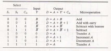
6


7 Logic Micro operation: There are 16 different logic operations that can be performed with two binary variables. The following table contains 16 columns F0 through F15 represents a truth table of one possible Boolean function for the two variables x an y. The 16 Boolean functions of two variables x and y are expressed in algebraic form as follows
8 Hardware Implementation: The following figure shows one stage of a circuit that generates the four basic logic micro operations. It consists of four gates and a multiplexer. Each of the four logic operations is generated through a gate that performs the required logic. The outputs of the gates are applied to the data inputs of the multiplexer. The two selection inputs s1 and s0 choose one of the data inputs of the multiplexer and direct its value to the output. Q3. Explain shift micro operation in detail with logic circuit. Shift micro operation is used for serial transfer of data. During a shift-left operation the serial input transfers a bit into the rightmost position. During a shift right operation the serial input transfers a bit into the leftmost position.there are three types of shifts: logical, circular and arithmetic. A logical shift is one that transfers 0 through the serial inputs. shl and shr are used for logical shift left and shift right micro operation. The symbolic representation is as follows
9 R1<-shl R1 R2<-shr R2 The above micro operation specify 1-bit shift to the left of the content of register R1 and a 1-bit shift to the right of the content of register R2.The bit transferred to the end position through the serial input is assumed to be 0 during a logical shift. The circular shift circulates the bits of the register around the two ends without loss of information. This is accomplished by connecting the serial output of the shift register to its serial input. The symbolic notation for circular shift is R<-cil R R<-cir R An arithmetic shift is a micro operation that shifts a signed binary number to the left or right. An arithmetic shift left multiplies a signed binary number by 2. An arithmetic shift-right divides the number by 2. Arithmetic shifts must leave the sign bit unchanged. The leftmost bit in a register holds the sign bit and the remaining bits hold the number. The sign bit is 0 for positive and 1 for negative. The following figure shows a typical register with n bits. Bit R n-1 holds the sign bit. The arithmetic shift-right leaves the sign bit unchanged and shifts the number to the right. The arithmetic shift left inserts a 0 into R 0 and shifts all other bits to the left. The initial bit of R n-1 is lost and replaced by the bit from R n-2. A sign reversal occurs if the bit in R n-1 changes in value after the shift. This happens in case of overflow. To check this flip-flop V s is used. If V s =0, there is no overflow but if V s =1, there is an over flow and a sign reversal occurs. Hardware implementation: Vs=R n-1 X-OR R n-2 A combinational circuit shifter can be constructed with multiplexers. The 4-bit shifter has four data inputs, A0 through A3 and four data outputs, H0 through H3.There are two serial inputs, one for shift left I L and shift right I R. When the selection input S=0 the input data are shifted right. When S=1 the data are shifted left. A shifter with n data inputs and outputs requires n multiplexers. The two serial inputs can be controlled by another multiplexer to provide the three possible types of shifts. The logic circuit and Boolean function r 4-bit shifter are as follows
10 Q4. A. Discuss program loops in assembly language. A program loop is a sequence of instruction that are executed many times each time with a different set of data.
 to A(1). The number -100 is stored in NBR.")
11 The address of first operand is stored 150 is stored in location ADS in line 13. The number of times the statement number 3 must be executed is 100, So -100 is stored in location NBR. The address of the first operand is transferred to location PTR. This corresponds to setting A(J) to A(1). The number -100 is stored in NBR. The address of first operand is transferred to location PTR. The location acts as counter. As the reaches zero the 100 operations will be completed and the program will exit from the loop.
12 The program loop specified by the DO statement is translated to the sequence of instructions listed in lines 7 through 10. Line 7 specifies an indirect ADD instruction because it has the symbol I. he address of the current operand is stored in location PTR. When this location is addressed indirectly the computer takes the content of PTR to be the address of the operand. As a result the operand in location 150 is added to the accumulator, Location PTR is incremented in line 9 and if nonzero the computer does not skip the next instruction. The next instruction is a branch instruction to the beginning of the loop. When location CTR reaches to zero the next instruction is skipped and line 11 and 12 are executed. The sum so formed in AC is stored in SUM and the computer halts. B) Discuss different types of memory The main memory is the central storage unit in computer system. It is a relatively large and fast memory used to store programs and data during the computer operation. The principal technology used for the main memory is based on semi conductor integrated circuits. Three are two types of memory primary memory and secondary memory. Primary memory stores current data and instructions and the secondary memory stores the rest. Primary memory is divided into RAM and ROM RAM: RAM stands for random access memory. The read and write memory of a computer is called RAM. It possesses random access property. RAM is a volatile memory. The information written into it is retained in it as long as the power supply is on. There are two important types of RAM : Dynamic RAM Static RAM Dynamic RAM: Dynamic RAM loses its stored information in a very short time even though the power supply is on. In a dynamic RAM a binary state is stored on the gate to source stray capacitor of transistor of the MOS memory circuit. The presence of charge is represented as 1 and the absence of charge is represented as 0. The charges leaks in a few millisecond. So dynamic RAM need to be refreshed
13 every millisecond. Dynamic RAMS are cheaper and have high packing density and moderate speed, They consumes less power. Dynamic RAM are written as DRAM. DRAM s are used for main memory. Static RAM: The static RAM consists of internal flip flops that stores binary information. Static RAM retains stored information only as long as the power supply is on. Static RAMs are costlier and consumes more power. They do not need refreshing circuitry. They have higher speed than dynamic RAM s.static RAM is written as SRAM. SRAM s are used for cache memory. ROM: ROM stands for Read only memory. It is non volatile memory. The information stored in it not lost even if the power supply goes off. It is used for permanent storage of information. The stored information can only be read from ROM s at the time of operation. Information cannot be written into a ROM by the user/ programmer. The content of ROM is decided at the time of manufacturing. ROM is placed in two broad categories Masked programmed: ROM in which contents are written at the time of IC manufacture are called mask-programmed. User programmed: Other types of ROMs are user programmed. Types of ROM: PROM: PROM is a programmable ROM.Its contents are decided by the user. The user can store permanent programs, data or any kind of information in a PROM. PROM s are once programmable; the user can write his information in a PROM only once. EPROM: An EPROM is an erasable PROM. The stored data in EPROMs can be erased by exposing it to high intensity short wave ultraviolet light for about 20 minutes. When an EPROM is exposed to ultra violet light the entire data are erased. The user cannot erase the contents of certain selected memory locations. EEPROM: EEPROM is an electrically erasable PROM. It is known as electrically alterable PROM. The chip can be reprogrammed on a byte by byte basis. Either a single byte or the entire chip can be erased in one operation.


14 The following figures shows an example of a 1024X8 memory constructed with 128X8 RAM chips and 512 X 8 POM chips. 5) Explain instruction pipeline in detail with flow chart. An instruction pipeline reads consecutive instructions from memory while previous instructions are being executed in other segments. This causes the instruction fetch and executes phases to overlap and perform simultaneous operations. In instruction pipeline the decoding of the instruction is combined with the calculation of effective address into one segment. Instruction execution and storing of instruction are combined into one segment. This reduces the instruction into four segments. The following figure shows how the instruction cycle in the CPU can be processes with a four segment pipeline. While an instruction is being executed in segment4, the next instruction in sequence is busy in fetching an operand from memory in segment 3. The effective address is calculated in a separate segment. Once in a while an instruction in the sequence may be a program control that causes a branch out of normal sequence. In that case the pending operations in the last two segments are completed and all information stored in the instruction buffer is deleted. The pipeline then restarts from the new address stored

15 in the program counter. Similarly an interrupt request, when acknowledged, it causes the pipeline to empty and restart again from a new address value. The segments of the instruction pipelining are FI, DA, FO & EX. The time in the horizontal axis is divided into steps of equal duration. The four segments are represented in the figure. FI= The segment that fetches an instruction. DA=The segment that decodes the instruction and calculates the effective address. FO=The segment that fetches the operant. Ex=The segment that executes the instruction.

16 Branch Instruction: In the absence of a branch instruction, each segment operates on different.thus in step 4 instruction 1 is being executed in segment EX; the operand for instruction 2 is being fetched in segment FO; instruction 3 is being decoded in segment DA; and instruction 4 is being fetched from memory in segment FI. Let us assume that instruction in 3 is a branch instruction. As soon as the instruction is decoded in segment DA in step 4, the transfer from FI to DA of the other instructions is halted until the branch instruction is executed in step 6. If the branch is taken, a new instruction is fetched in step 7. If the branch is not taken, the instruction fetched previously in step 4 can be used. The pipeline then continues until a new branch instruction is encountered. Q6. Discuss the design of accumulator logic. In an accumulator design he adder and logic circuits has three sets of inputs. One set of 16 inputs comes from the outputs of AC. Another set of 16 inputs comes from the data register DR. A third set of eight inputs comes from the input register INPR. The outputs of the adder and logic circuits provide gates for controlling the LD, INR and CLR in the register and for controlling the operation of the adder and logic circuit. The circuit associated with AC register is shown below.

17 In order to design the logic associated with AC all statements that changes the content of Ac is needed. The statements are as follows. The gate structure of AC register from the above function table is as follows

18 Q7. Explain the concept of DMA in detail. Direct access Memory The transfer of data between a fast storage device and memory is always limited by the speed of the CPU. Removing the CPU from the path and letting the peripheral device to manage the memory buses directly is known as direct access memory. In DMA CPU is idle and has no control of the memory buses. A DMA
19 controller takes over the buses to manage the transfer directly between the I/O device and memory. The following figure shows two control signals in the CPU that facilitate the DMA transfer. The bus request (BR) input is the external DMA that the buses used by the DMA controller to request the CPU to relinquish control of the buses. When this input is active CPU terminates the execution of the current instruction and places the address bus, the data bus, and the read and writes lines into a high impedance state. The CPU activates bus grant (BG) output to inform the external DMA that buses are free. The DMA that originates the bus request can now take control of the buses to conduct memory transfer without processor intervention. When the DMA terminates the transfer, it disables the bus request line. The CPU disables the bus grant, takes control of the buses, and returns to its normal operation. DMA controller: The DMA controller needs an address register, a word count register and a set of address lines for communication. The unit communicates with CPU via the data bus and control lines. The register in the DMA are selected by the CPU through the address bus by enabling the DS (DMA select) and RS (Register select) inputs. The read and write inputs are bi directional. When the BG input is 0 the CPU can communicates with the DMA registers through the data bus to read from or write to the DMA register. When BG=1, the CPU frees the bus and DMA can communicate directly with the memory. Following figure shows block diagram of DMA controller
20 DMA controller has three register: Address register: The address register contains an address to specify the desired location in memory. The address register is incremented after each word is transferred to memory Word count register: It holds the number of words to be trans transfer and internally tested for zero. This register is decremented by one after each word transfer and internally tested for zero. Control register: The control register specifies the mode of transfer. DMA transfer: The CPU initializes the DMA by sending the following information 1) The starting address of the memory block where data are available or stored 2) The word count, which is the number of words in the memory block 3) Control to specify the mode of transfer such as read or write 4) A control to start the DMA transfer. The following figure shows DMA transfer in a computer system. When the peripheral device sends a DMA request DMA controller activates BR line.the CPU responds with BG line.the DMA sends acknowledgement to the peripheral

21 device. When BG=0 CPU communicates with DMA. When BG=1 DMA takes the control. Q8. What do you mean by page replacement? Explain different types of page replacement with examples. When a page fault occurs, the OS loads the faulted page from disk into a page frame memory. If the processor has used all frames the OS must replace a page for each page faulted in. This is known as page replacement. Page replacement algorithm determines the page to be replaced. There are three types of page replacement algorithms. 1) FCFS page replacement algorithm using 3 frames: In FIFO the algorithm selects for replacement the page which has been used for a longest period of time. Total number of page fault for the following is 15.


22 2) Optimal page replacement algorithm by using 3 frames: In optimal the algorithm selects the page which will not be used for a longest period of time. Total number of page fault for the following example is 9. 3) LRU page replacement algorithm by using 3 frames: In LRU the algorithm selects the page that has been least recently used. Total number of page fault for the following example is 12.
COA. Prepared By: Dhaval R. Patel Page 1. Q.1 Define MBR.
 Q.1 Define MBR. MBR( Memory buffer register) A Memory Buffer Register (MBR) is the register in a computers processor that stores the data being transferred to and from the devices It allowing the processor
COMPUTER ARCHITECTURE AND ORGANIZATION Register Transfer and Micro-operations 1. Introduction A digital system is an interconnection of digital
 Register Transfer and Micro-operations 1. Introduction A digital system is an interconnection of digital hardware modules that accomplish a specific information-processing task. Digital systems vary in
csitnepal Unit 3 Basic Computer Organization and Design
 Unit 3 Basic Computer Organization and Design Introduction We introduce here a basic computer whose operation can be specified by the resister transfer statements. Internal organization of the computer
UNIT-III REGISTER TRANSFER LANGUAGE AND DESIGN OF CONTROL UNIT
 UNIT-III 1 KNREDDY UNIT-III REGISTER TRANSFER LANGUAGE AND DESIGN OF CONTROL UNIT Register Transfer: Register Transfer Language Register Transfer Bus and Memory Transfers Arithmetic Micro operations Logic
REGISTER TRANSFER LANGUAGE
 REGISTER TRANSFER LANGUAGE The operations executed on the data stored in the registers are called micro operations. Classifications of micro operations Register transfer micro operations Arithmetic micro
CHAPTER 5 Basic Organization and Design Outline Instruction Codes Computer Registers Computer Instructions Timing and Control Instruction Cycle
 CS 224: Computer Organization S.KHABET CHAPTER 5 Basic Organization and Design Outline Instruction Codes Computer Registers Computer Instructions Timing and Control Instruction Cycle Memory Reference Instructions
CHAPTER SIX BASIC COMPUTER ORGANIZATION AND DESIGN
 CHAPTER SIX BASIC COMPUTER ORGANIZATION AND DESIGN 6.1. Instruction Codes The organization of a digital computer defined by: 1. The set of registers it contains and their function. 2. The set of instructions
COMPUTER ORGANIZATION
 COMPUTER ORGANIZATION INDEX UNIT-II PPT SLIDES Srl. No. Module as per Session planner Lecture No. PPT Slide No. 1. Register Transfer language 2. Register Transfer Bus and memory transfers 3. Arithmetic
UNIT - V MEMORY P.VIDYA SAGAR ( ASSOCIATE PROFESSOR) Department of Electronics and Communication Engineering, VBIT
 Department of Electronics and Communication Engineering, VBIT") UNIT - V MEMORY P.VIDYA SAGAR ( ASSOCIATE PROFESSOR) contents Memory: Introduction, Random-Access memory, Memory decoding, ROM, Programmable Logic Array, Programmable Array Logic, Sequential programmable
UNIT - V MEMORY P.VIDYA SAGAR ( ASSOCIATE PROFESSOR) contents Memory: Introduction, Random-Access memory, Memory decoding, ROM, Programmable Logic Array, Programmable Array Logic, Sequential programmable
2 MARKS Q&A 1 KNREDDY UNIT-I
 2 MARKS Q&A 1 KNREDDY UNIT-I 1. What is bus; list the different types of buses with its function. A group of lines that serves as a connecting path for several devices is called a bus; TYPES: ADDRESS BUS,
Register Transfer and Micro-operations
 Register Transfer Language Register Transfer Bus Memory Transfer Micro-operations Some Application of Logic Micro Operations Register Transfer and Micro-operations Learning Objectives After reading this
SECTION-A
 M.Sc(CS) ( First Semester) Examination,2013 Digital Electronics Paper: Fifth ------------------------------------------------------------------------------------- SECTION-A I) An electronics circuit/ device
Unit II Basic Computer Organization
 1. Define the term. Internal Organization-The internal organization of a digital system is defined by the sequence of microoperations it performs on data stored in its registers. Program- A program is
BASIC COMPUTER ORGANIZATION AND DESIGN
 1 BASIC COMPUTER ORGANIZATION AND DESIGN Instruction Codes Computer Registers Computer Instructions Timing and Control Instruction Cycle Memory Reference Instructions Input-Output and Interrupt Complete
Computer architecture Assignment 3
 Computer architecture Assignment 3 1- An instruction at address 14E in the basic computer has I=0, an operation code of the AND instruction, and an address part equal to 109(all numbers are in hexadecimal).
THE MICROCOMPUTER SYSTEM CHAPTER - 2
 THE MICROCOMPUTER SYSTEM CHAPTER - 2 20 2.1 GENERAL ASPECTS The first computer was developed using vacuum tubes. The computers thus developed were clumsy and dissipating more power. After the invention
Computer Organization and Assembly Language (CS-506)
") Computer Organization and Assembly Language (CS-506) Muhammad Zeeshan Haider Ali Lecturer ISP. Multan ali.zeeshan04@gmail.com https://zeeshanaliatisp.wordpress.com/ Lecture 2 Memory Organization and Structure
Computer Organization and Assembly Language (CS-506) Muhammad Zeeshan Haider Ali Lecturer ISP. Multan ali.zeeshan04@gmail.com https://zeeshanaliatisp.wordpress.com/ Lecture 2 Memory Organization and Structure
5-1 Instruction Codes
 Chapter 5: Lo ai Tawalbeh Basic Computer Organization and Design 5-1 Instruction Codes The Internal organization of a digital system is defined by the sequence of microoperations it performs on data stored
UNIT-II. Part-2: CENTRAL PROCESSING UNIT
 Page1 UNIT-II Part-2: CENTRAL PROCESSING UNIT Stack Organization Instruction Formats Addressing Modes Data Transfer And Manipulation Program Control Reduced Instruction Set Computer (RISC) Introduction:
CREATED BY M BILAL & Arslan Ahmad Shaad Visit:
 CREATED BY M BILAL & Arslan Ahmad Shaad Visit: www.techo786.wordpress.com Q1: Define microprocessor? Short Questions Chapter No 01 Fundamental Concepts Microprocessor is a program-controlled and semiconductor
Chapter 5. Computer Architecture Organization and Design. Computer System Architecture Database Lab, SANGJI University
 Chapter 5. Computer Architecture Organization and Design Computer System Architecture Database Lab, SANGJI University Computer Architecture Organization and Design Instruction Codes Computer Registers
Computer Architecture
 Computer Architecture Lecture 1: Digital logic circuits The digital computer is a digital system that performs various computational tasks. Digital computers use the binary number system, which has two
Computer Organization (Autonomous)
") Computer Organization (Autonomous) UNIT II Sections - A & D Prepared by Anil Kumar Prathipati, Asst. Prof., Dept. of CSE. SYLLABUS Basic Computer Organization and Design: Instruction codes Stored Program
Computer Organization (Autonomous) UNIT II Sections - A & D Prepared by Anil Kumar Prathipati, Asst. Prof., Dept. of CSE. SYLLABUS Basic Computer Organization and Design: Instruction codes Stored Program
BASIC COMPUTER ORGANIZATION AND DESIGN
 BASIC COMPUTER ORGANIZATION AND DESIGN Instruction Codes Computer Registers Computer Instructions Timing and Control Instruction Cycle Memory Reference Instructions Input-Output and Interrupt Complete
 Chapter 1 Microprocessor architecture ECE 3120 Dr. Mohamed Mahmoud http://iweb.tntech.edu/mmahmoud/ mmahmoud@tntech.edu Outline 1.1 Computer hardware organization 1.1.1 Number System 1.1.2 Computer hardware
Basic Computer Organization - Designing your first computer. Acknowledgment: Most of the slides are adapted from Prof. Hyunsoo Yoon s slides.
 Basic Computer Organization - Designing your first computer Acknowledgment: Most of the slides are adapted from Prof. Hyunsoo Yoon s slides. 1 This week- BASIC COMPUTER ORGANIZATION AND DESIGN Instruction
BASIC COMPUTER ORGANIZATION AND DESIGN
 1 BASIC COMPUTER ORGANIZATION AND DESIGN Instruction Codes Computer Registers Computer Instructions Timing and Control Instruction Cycle Memory Reference Instructions Input-Output and Interrupt Complete
Darshan Institute of Engineering & Technology for Diploma Studies Unit - 1
 Darshan Institute of Engineering & Technology for Diploma Studies Unit - 1 1. Draw and explain 4 bit binary arithmetic or adder circuit diagram. A binary parallel adder is digital function that produces
Introduction. Machine Language. Assembly Language. Assembler. Program Loops. Programming Arithmetic and Logic Operations.
 Computer System AA rc hh ii tec ture( 66 )) PROGRAMMING THE BASIC COMPUTER Introduction Machine Language Assembly Language Assembler Program Loops Programming Arithmetic and Logic Operations Subroutines
1. INTRODUCTION TO MICROPROCESSOR AND MICROCOMPUTER ARCHITECTURE:
 1. INTRODUCTION TO MICROPROCESSOR AND MICROCOMPUTER ARCHITECTURE: A microprocessor is a programmable electronics chip that has computing and decision making capabilities similar to central processing unit
Concept of Memory. The memory of computer is broadly categories into two categories:
 Concept of Memory We have already mentioned that digital computer works on stored programmed concept introduced by Von Neumann. We use memory to store the information, which includes both program and data.
Logic and Computer Design Fundamentals. Chapter 8 Memory Basics
 Logic and Computer Design Fundamentals Memory Basics Overview Memory definitions Random Access Memory (RAM) Static RAM (SRAM) integrated circuits Arrays of SRAM integrated circuits Dynamic RAM (DRAM) Read
COMPUTER ORGANIZATION AND ARCHITECTURE
 Page 1 1. Which register store the address of next instruction to be executed? A) PC B) AC C) SP D) NONE 2. How many bits are required to address the 128 words of memory? A) 7 B) 8 C) 9 D) NONE 3. is the
PART A (22 Marks) 2. a) Briefly write about r's complement and (r-1)'s complement. [8] b) Explain any two ways of adding decimal numbers.
![PART A (22 Marks) 2. a) Briefly write about r's complement and (r-1)'s complement. [8] b) Explain any two ways of adding decimal numbers.](/thumbs/96/128058841.jpg "PART A (22 Marks) 2. a) Briefly write about r's complement and (r-1)'s complement. [8] b) Explain any two ways of adding decimal numbers.") Set No. 1 IV B.Tech I Semester Supplementary Examinations, March - 2017 COMPUTER ARCHITECTURE & ORGANIZATION (Common to Electronics & Communication Engineering and Electronics & Time: 3 hours Max. Marks:
Set No. 1 IV B.Tech I Semester Supplementary Examinations, March - 2017 COMPUTER ARCHITECTURE & ORGANIZATION (Common to Electronics & Communication Engineering and Electronics & Time: 3 hours Max. Marks:
Read and Write Cycles
 Read and Write Cycles The read cycle is shown. Figure 41.1a. The RAS and CAS signals are activated one after the other to latch the multiplexed row and column addresses respectively applied at the multiplexed
Computer Organization and Design
 CSE211 Computer Organization and Design Lecture : 3 Tutorial: 1 Practical: 0 Credit: 4 KIDS Labs 1 Unit 1 : Basics of Digital Electronics Introduction Logic Gates Flip Flops Decoder Encoder Multiplexers
5 Computer Organization
 5 Computer Organization 5.1 Foundations of Computer Science ã Cengage Learning Objectives After studying this chapter, the student should be able to: q List the three subsystems of a computer. q Describe
CS 265. Computer Architecture. Wei Lu, Ph.D., P.Eng.
 CS 265 Computer Architecture Wei Lu, Ph.D., P.Eng. Part 4: Memory Organization Our goal: understand the basic types of memory in computer understand memory hierarchy and the general process to access memory
UNIT:2 BASIC COMPUTER ORGANIZATION AND DESIGN
 1 UNIT:2 BASIC COMPUTER ORGANIZATION AND DESIGN BASIC COMPUTER ORGANIZATION AND DESIGN 2.1 Instruction Codes 2.2 Computer Registers AC or Accumulator, Data Register or DR, the AR or Address Register, program
Computer Architecture: Part V. First Semester 2013 Department of Computer Science Faculty of Science Chiang Mai University
 Computer Architecture: Part V First Semester 2013 Department of Computer Science Faculty of Science Chiang Mai University Outline Addition and Subtraction Multiplication Algorithm Array Multiplier Peripheral
UNIT I STRUCTURE OF COMPUTERS
 Unit I UNIT I STRUCTURE OF COMPUTERS 1.1 Digital Computer The digital computer is a digital system that performs various computational tasks. The word digital implies that the information in the computer
MULTIMEDIA COLLEGE JALAN GURNEY KIRI KUALA LUMPUR
 STUDENT IDENTIFICATION NO MULTIMEDIA COLLEGE JALAN GURNEY KIRI 54100 KUALA LUMPUR SECOND SEMESTER FINAL EXAMINATION, 2013/2014 SESSION ITC2223 COMPUTER ORGANIZATION & ARCHITECTURE DSEW-E-F 1/13 18 FEBRUARY
Semiconductor Memories: RAMs and ROMs
 Semiconductor Memories: RAMs and ROMs Lesson Objectives: In this lesson you will be introduced to: Different memory devices like, RAM, ROM, PROM, EPROM, EEPROM, etc. Different terms like: read, write,
Computer Architecture Programming the Basic Computer
 4. The Execution of the EXCHANGE Instruction The EXCHANGE routine reads the operand from the effective address and places it in DR. The contents of DR and AC are interchanged in the third microinstruction.
Lecture Objectives. Introduction to Computing Chapter 0. Topics. Numbering Systems 04/09/2017
 Lecture Objectives Introduction to Computing Chapter The AVR microcontroller and embedded systems using assembly and c Students should be able to: Convert between base and. Explain the difference between
EE 308: Microcontrollers
 EE 308: Microcontrollers AVR Architecture Aly El-Osery Electrical Engineering Department New Mexico Institute of Mining and Technology Socorro, New Mexico, USA January 23, 2018 Aly El-Osery (NMT) EE 308:
Summer 2003 Lecture 18 07/09/03
 Summer 2003 Lecture 18 07/09/03 NEW HOMEWORK Instruction Execution Times: The 8088 CPU is a synchronous machine that operates at a particular clock frequency. In the case of the original IBM PC, that clock
For Example: P: LOAD 5 R0. The command given here is used to load a data 5 to the register R0.
 Register Transfer Language Computers are the electronic devices which have several sets of digital hardware which are inter connected to exchange data. Digital hardware comprises of VLSI Chips which are
CHETTINAD COLLEGE OF ENGINEERING AND TECHNOLOGY COMPUTER ARCHITECURE- III YEAR EEE-6 TH SEMESTER 16 MARKS QUESTION BANK UNIT-1
 CHETTINAD COLLEGE OF ENGINEERING AND TECHNOLOGY COMPUTER ARCHITECURE- III YEAR EEE-6 TH SEMESTER 16 MARKS QUESTION BANK UNIT-1 Data representation: (CHAPTER-3) 1. Discuss in brief about Data types, (8marks)
3. Controtlto specify the mode of transfer such as read or write 4. A control to start the DMA transfer
 DMA Controller The DMA controller needs the usual circuits of an interface to communicate the CPU and 10 device. In addition, it needs an address register, a word count register, and a set of address lines.
Modes of Transfer. Interface. Data Register. Status Register. F= Flag Bit. Fig. (1) Data transfer from I/O to CPU
 Data transfer from I/O to CPU") Modes of Transfer Data transfer to and from peripherals may be handled in one of three possible modes: A. Programmed I/O B. Interrupt-initiated I/O C. Direct memory access (DMA) A) Programmed I/O Programmed
Modes of Transfer Data transfer to and from peripherals may be handled in one of three possible modes: A. Programmed I/O B. Interrupt-initiated I/O C. Direct memory access (DMA) A) Programmed I/O Programmed
Basic Computer Organization and Design Part 2/3
 Basic Computer Organization and Design Part 2/3 Adapted by Dr. Adel Ammar Computer Organization Basic Computer Instructions Basic Computer Instruction Format Memory-Reference Instructions (OP-code = 000
EC2304-MICROPROCESSOR AND MICROCONROLLERS 2 marks questions and answers UNIT-I
 EC2304-MICROPROCESSOR AND MICROCONROLLERS 2 marks questions and answers 1. Define microprocessors? UNIT-I A semiconductor device(integrated circuit) manufactured by using the LSI technique. It includes
Chapter 3 : Control Unit
 3.1 Control Memory Chapter 3 Control Unit The function of the control unit in a digital computer is to initiate sequences of microoperations. When the control signals are generated by hardware using conventional
COMP3221: Microprocessors and. and Embedded Systems. Overview. Lecture 23: Memory Systems (I)
") COMP3221: Microprocessors and Embedded Systems Lecture 23: Memory Systems (I) Overview Memory System Hierarchy RAM, ROM, EPROM, EEPROM and FLASH http://www.cse.unsw.edu.au/~cs3221 Lecturer: Hui Wu Session
COMP3221: Microprocessors and Embedded Systems Lecture 23: Memory Systems (I) Overview Memory System Hierarchy RAM, ROM, EPROM, EEPROM and FLASH http://www.cse.unsw.edu.au/~cs3221 Lecturer: Hui Wu Session
SYLLABUS. osmania university CHAPTER - 1 : REGISTER TRANSFER LANGUAGE AND MICRO OPERATION CHAPTER - 2 : BASIC COMPUTER
 Contents i SYLLABUS osmania university UNIT - I CHAPTER - 1 : REGISTER TRANSFER LANGUAGE AND MICRO OPERATION Difference between Computer Organization and Architecture, RTL Notation, Common Bus System using
The x86 Microprocessors. Introduction. The 80x86 Microprocessors. 1.1 Assembly Language
 The x86 Microprocessors Introduction 1.1 Assembly Language Numbering and Coding Systems Human beings use the decimal system (base 10) Decimal digits: 0, 1, 2, 3, 4, 5, 6, 7, 8, 9 Computer systems use the
CHAPTER 4: Register Transfer Language and Microoperations
 CS 224: Computer Organization S.KHABET CHAPTER 4: Register Transfer Language and Microoperations Outline Register Transfer Language Register Transfer Bus and Memory Transfers Arithmetic Microoperations
INTELLIGENCE PLUS CHARACTER - THAT IS THE GOAL OF TRUE EDUCATION UNIT-I
 UNIT-I 1. List and explain the functional units of a computer with a neat diagram 2. Explain the computer levels of programming languages 3. a) Explain about instruction formats b) Evaluate the arithmetic
MICROPROCESSOR MCQs. 1) What does the microprocessor comprise of? a. Register section b. One or more ALU c. Control unit d.
 What does the microprocessor comprise of? a. Register section b. One or more ALU c. Control unit d.") 1) What does the microprocessor comprise of? a. Register section b. One or more ALU c. Control unit 2) What is stored by a register? a. data b. operands c. memory MICROPROCESSOR MCQs 3) Accumulator based
1) What does the microprocessor comprise of? a. Register section b. One or more ALU c. Control unit 2) What is stored by a register? a. data b. operands c. memory MICROPROCESSOR MCQs 3) Accumulator based
MAHALAKSHMI ENGINEERING COLLEGE TIRUCHIRAPALLI UNIT I THE 8085 & 8086 MICROPROCESSORS. PART A (2 Marks)
") MAHALAKSHMI ENGINEERING COLLEGE TIRUCHIRAPALLI-621213. UNIT I THE 8085 & 8086 MICROPROCESSORS PART A (2 Marks) 1. Give the significance of SIM and RIM instruction available in 8085. [NOV/DEC 2006] Instruction
MAHALAKSHMI ENGINEERING COLLEGE TIRUCHIRAPALLI-621213. UNIT I THE 8085 & 8086 MICROPROCESSORS PART A (2 Marks) 1. Give the significance of SIM and RIM instruction available in 8085. [NOV/DEC 2006] Instruction
Lecture-7 Characteristics of Memory: In the broad sense, a microcomputer memory system can be logically divided into three groups: 1) Processor
 Processor") Lecture-7 Characteristics of Memory: In the broad sense, a microcomputer memory system can be logically divided into three groups: 1) Processor memory 2) Primary or main memory 3) Secondary memory Processor
Lecture-7 Characteristics of Memory: In the broad sense, a microcomputer memory system can be logically divided into three groups: 1) Processor memory 2) Primary or main memory 3) Secondary memory Processor
TYPICAL QUESTIONS & ANSWERS
 TYPICAL QUESTIONS & ANSWERS PART-I Each Question carries 2 marks. OBJECTIVE TYPE QUESTIONS Choose the correct or best alternative in the following: Q.1 In Reverse Polish notation, expression A*B+C*D is
The CPU and Memory. How does a computer work? How does a computer interact with data? How are instructions performed? Recall schematic diagram:
 The CPU and Memory How does a computer work? How does a computer interact with data? How are instructions performed? Recall schematic diagram: 1 Registers A register is a permanent storage location within
UNIT-V MEMORY ORGANIZATION
 UNIT-V MEMORY ORGANIZATION 1 The main memory of a computer is semiconductor memory.the main memory unit is basically consists of two kinds of memory: RAM (RWM):Random access memory; which is volatile in
REGISTER TRANSFER AND MICROOPERATIONS
 1 REGISTER TRANSFER AND MICROOPERATIONS Register Transfer Language Register Transfer Bus and Memory Transfers Arithmetic Microoperations Logic Microoperations Shift Microoperations Arithmetic Logic Shift
Embedded Systems Design: A Unified Hardware/Software Introduction. Outline. Chapter 5 Memory. Introduction. Memory: basic concepts
 Hardware/Software Introduction Chapter 5 Memory Outline Memory Write Ability and Storage Permanence Common Memory Types Composing Memory Memory Hierarchy and Cache Advanced RAM 1 2 Introduction Memory:
Embedded Systems Design: A Unified Hardware/Software Introduction. Chapter 5 Memory. Outline. Introduction
 Hardware/Software Introduction Chapter 5 Memory 1 Outline Memory Write Ability and Storage Permanence Common Memory Types Composing Memory Memory Hierarchy and Cache Advanced RAM 2 Introduction Embedded
Computer Organisation CS303
 Computer Organisation CS303 Module Period Assignments 1 Day 1 to Day 6 1. Write a program to evaluate the arithmetic statement: X=(A-B + C * (D * E-F))/G + H*K a. Using a general register computer with
Microprocessors/Microcontrollers
 Microprocessors/Microcontrollers A central processing unit (CPU) fabricated on one or more chips, containing the basic arithmetic, logic, and control elements of a computer that are required for processing
1. Define Peripherals. Explain I/O Bus and Interface Modules. Peripherals: Input-output device attached to the computer are also called peripherals.
 1. Define Peripherals. Explain I/O Bus and Interface Modules. Peripherals: Input-output device attached to the computer are also called peripherals. A typical communication link between the processor and
Digital System Design Using Verilog. - Processing Unit Design
 Digital System Design Using Verilog - Processing Unit Design 1.1 CPU BASICS A typical CPU has three major components: (1) Register set, (2) Arithmetic logic unit (ALU), and (3) Control unit (CU) The register
Blog - https://anilkumarprathipati.wordpress.com/
 Control Memory 1. Introduction The function of the control unit in a digital computer is to initiate sequences of microoperations. When the control signals are generated by hardware using conventional
8051 INTERFACING TO EXTERNAL MEMORY
 8051 INTERFACING TO EXTERNAL MEMORY Memory Capacity The number of bits that a semiconductor memory chip can store Called chip capacity It can be in units of Kbits (kilobits), Mbits (megabits), and so on
CHAPTER SEVEN PROGRAMMING THE BASIC COMPUTER
 CHAPTER SEVEN 71 Introduction PROGRAMMING THE BASIC COMPUTER A computer system as it was mentioned before in chapter 1, it is subdivided into two functional parts: 1 Hardware, which consists of all physical
SAE5C Computer Organization and Architecture. Unit : I - V
 SAE5C Computer Organization and Architecture Unit : I - V UNIT-I Evolution of Pentium and Power PC Evolution of Computer Components functions Interconnection Bus Basics of PCI Memory:Characteristics,Hierarchy
1 MALP ( ) Unit-1. (1) Draw and explain the internal architecture of 8085.
 Unit-1. (1) Draw and explain the internal architecture of 8085.") (1) Draw and explain the internal architecture of 8085. The architecture of 8085 Microprocessor is shown in figure given below. The internal architecture of 8085 includes following section ALU-Arithmetic
(1) Draw and explain the internal architecture of 8085. The architecture of 8085 Microprocessor is shown in figure given below. The internal architecture of 8085 includes following section ALU-Arithmetic
UNIT:4 MEMORY ORGANIZATION
 1 UNIT:4 MEMORY ORGANIZATION TOPICS TO BE COVERED. 4.1 Memory Hierarchy 4.2 Memory Classification 4.3 RAM,ROM,PROM,EPROM 4.4 Main Memory 4.5Auxiliary Memory 4.6 Associative Memory 4.7 Cache Memory 4.8
COMP2121: Microprocessors and Interfacing. Introduction to Microprocessors
 COMP2121: Microprocessors and Interfacing Introduction to Microprocessors http://www.cse.unsw.edu.au/~cs2121 Lecturer: Hui Wu Session 2, 2017 1 1 Contents Processor architectures Bus Memory hierarchy 2
MEMORY BHARAT SCHOOL OF BANKING- VELLORE
 A memory is just like a human brain. It is used to store data and instructions. Computer memory is the storage space in computer where data is to be processed and instructions required for processing are
Microcomputer Architecture and Programming
 IUST-EE (Chapter 1) Microcomputer Architecture and Programming 1 Outline Basic Blocks of Microcomputer Typical Microcomputer Architecture The Single-Chip Microprocessor Microprocessor vs. Microcontroller
MICROPROGRAMMED CONTROL
 MICROPROGRAMMED CONTROL Hardwired Control Unit: When the control signals are generated by hardware using conventional logic design techniques, the control unit is said to be hardwired. Micro programmed
CS 320 February 2, 2018 Ch 5 Memory
 CS 320 February 2, 2018 Ch 5 Memory Main memory often referred to as core by the older generation because core memory was a mainstay of computers until the advent of cheap semi-conductor memory in the
Computer Architecture
 http://www.bsccsit.com/ Computer Architecture CSC. 201 Third Semester Prepared By: Arjun Singh Saud Special thanks to Mr. Arjun Singh Saud for providing this valuable note! Chapter 1 Data representation
Chapter 1. Microprocessor architecture ECE Dr. Mohamed Mahmoud.
 Chapter 1 Microprocessor architecture ECE 3130 Dr. Mohamed Mahmoud The slides are copyright protected. It is not permissible to use them without a permission from Dr Mahmoud http://www.cae.tntech.edu/~mmahmoud/
Blog -
 . Instruction Codes Every different processor type has its own design (different registers, buses, microoperations, machine instructions, etc) Modern processor is a very complex device It contains Many
Computer Systems Organization
 The IAS (von Neumann) Machine Computer Systems Organization Input Output Equipment Stored Program concept Main memory storing programs and data ALU operating on binary data Control unit interpreting instructions
Introduction to Embedded Systems and Chapter 1: Introduction to HCS12/MC9S12. EE383: Introduction to Embedded Systems University of Kentucky
 Introduction to Embedded Systems and Chapter 1: Introduction to HCS12/MC9S12 EE383: Introduction to Embedded Systems University of Kentucky Samir Rawashdeh With slides based on material by H. Huang Delmar
JNTUWORLD. 1. Discuss in detail inter processor arbitration logics and procedures with necessary diagrams? [15]
![JNTUWORLD. 1. Discuss in detail inter processor arbitration logics and procedures with necessary diagrams? [15]](/thumbs/96/128058746.jpg "JNTUWORLD. 1. Discuss in detail inter processor arbitration logics and procedures with necessary diagrams? [15]") Code No: 09A50402 R09 Set No. 2 1. Discuss in detail inter processor arbitration logics and procedures with necessary diagrams? [15] 2. (a) Discuss asynchronous serial transfer concept? (b) Explain in
Code No: 09A50402 R09 Set No. 2 1. Discuss in detail inter processor arbitration logics and procedures with necessary diagrams? [15] 2. (a) Discuss asynchronous serial transfer concept? (b) Explain in
Programming Level A.R. Hurson Department of Computer Science Missouri University of Science & Technology Rolla, Missouri
 Programming Level A.R. Hurson Department of Computer Science Missouri University of Science & Technology Rolla, Missouri 65409 hurson@mst.edu A.R. Hurson 1 Programming Level Computer: A computer with a
Faculty of Engineering Systems & Biomedical Dept. First Year Cairo University Sheet 6 Computer I
 aculty of Engineering Systems & Biomedical Dept. irst Year Cairo University Sheet 6 Computer I 1. Choose rue or alse for each of the following statements a) In a direct addressing mode instruction, the
Microcontroller Systems. ELET 3232 Topic 11: General Memory Interfacing
 Microcontroller Systems ELET 3232 Topic 11: General Memory Interfacing 1 Objectives To become familiar with the concepts of memory expansion and the data and address bus To design embedded systems circuits
Computer Organization (Autonomous)
") Computer Organization (Autonomous) UNIT I Sections - A & D Prepared by Anil Kumar Prathipati, Asst. Prof., Dept. of CSE. SYLLABUS Introduction: Types of Computers, Functional units of Basic Computer (Block
Computer Organization (Autonomous) UNIT I Sections - A & D Prepared by Anil Kumar Prathipati, Asst. Prof., Dept. of CSE. SYLLABUS Introduction: Types of Computers, Functional units of Basic Computer (Block
a) Memory management unit b) CPU c) PCI d) None of the mentioned
 Memory management unit b) CPU c) PCI d) None of the mentioned") 1. CPU fetches the instruction from memory according to the value of a) program counter b) status register c) instruction register d) program status word 2. Which one of the following is the address generated
1. CPU fetches the instruction from memory according to the value of a) program counter b) status register c) instruction register d) program status word 2. Which one of the following is the address generated
COSC 243. Computer Architecture 1. COSC 243 (Computer Architecture) Lecture 6 - Computer Architecture 1 1
 Lecture 6 - Computer Architecture 1 1") COSC 243 Computer Architecture 1 COSC 243 (Computer Architecture) Lecture 6 - Computer Architecture 1 1 Overview Last Lecture Flip flops This Lecture Computers Next Lecture Instruction sets and addressing
COSC 243 Computer Architecture 1 COSC 243 (Computer Architecture) Lecture 6 - Computer Architecture 1 1 Overview Last Lecture Flip flops This Lecture Computers Next Lecture Instruction sets and addressing
STRUCTURE OF DESKTOP COMPUTERS
 Page no: 1 UNIT 1 STRUCTURE OF DESKTOP COMPUTERS The desktop computers are the computers which are usually found on a home or office desk. They consist of processing unit, storage unit, visual display
TYPES OF INTERRUPTS: -
 There are 3 types of interrupts. TYPES OF INTERRUPTS: - External Interrupts. Internal Interrupts. Software interrupts. Hardware Interrupts (1) External interrupts come from I/O devices, from a timing device
Computer Architecture and Organization: L04: Micro-operations
 Computer Architecture and Organization: L4: Micro-operations By: A. H. Abdul Hafez Abdul.hafez@hku.edu.tr, ah.abdulhafez@gmail.com, hafez@research.iiit.ac.in 1 Outlines 1. Arithmetic microoperation 2.
Question Bank Microprocessor and Microcontroller
 QUESTION BANK - 2 PART A 1. What is cycle stealing? (K1-CO3) During any given bus cycle, one of the system components connected to the system bus is given control of the bus. This component is said to
Combinational and sequential circuits (learned in Chapters 1 and 2) can be used to create simple digital systems.
 can be used to create simple digital systems.") REGISTER TRANSFER AND MICROOPERATIONS Register Transfer Language Register Transfer Bus and Memory Transfers Arithmetic Microoperations Logic Microoperations Shift Microoperations Arithmetic Logic Shift
REGISTER TRANSFER AND MICROOPERATIONS Register Transfer Language Register Transfer Bus and Memory Transfers Arithmetic Microoperations Logic Microoperations Shift Microoperations Arithmetic Logic Shift