Programmable Logic Devices UNIT II DIGITAL SYSTEM DESIGN
|
|
|
- Easter Evans
- 5 years ago
- Views:
Transcription
1 Programmable Logic Devices UNIT II DIGITAL SYSTEM DESIGN
2 2
3 3
4 4
5 5
6 6
7 7
8 8
9 9

10
11
12 2
13 3
14 4
15 5
16 6
17 7
18 8
19 9
20 2
21 Implementation in Sequential Logic 2
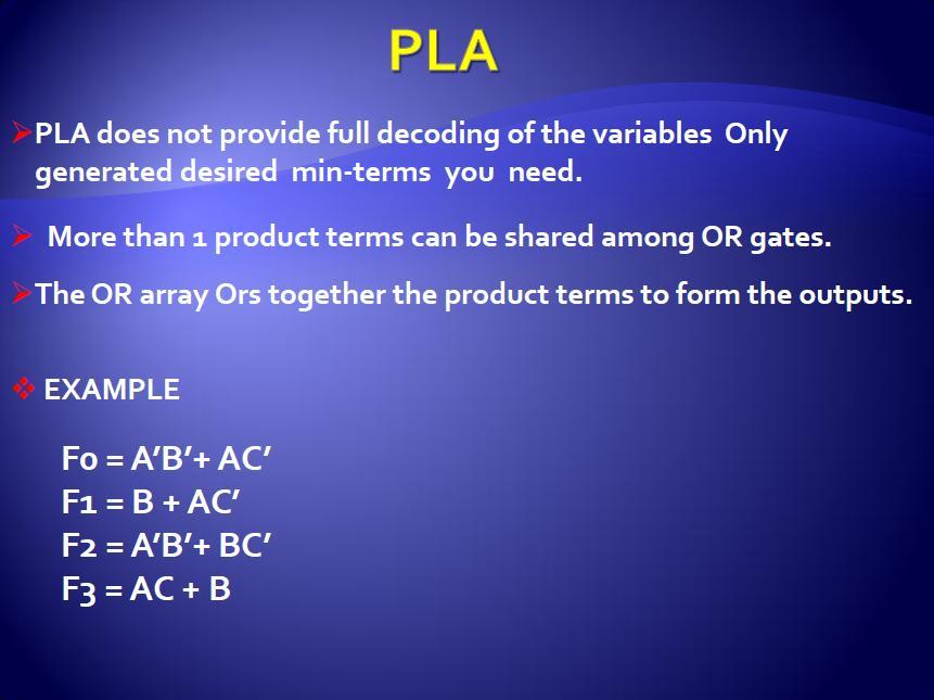
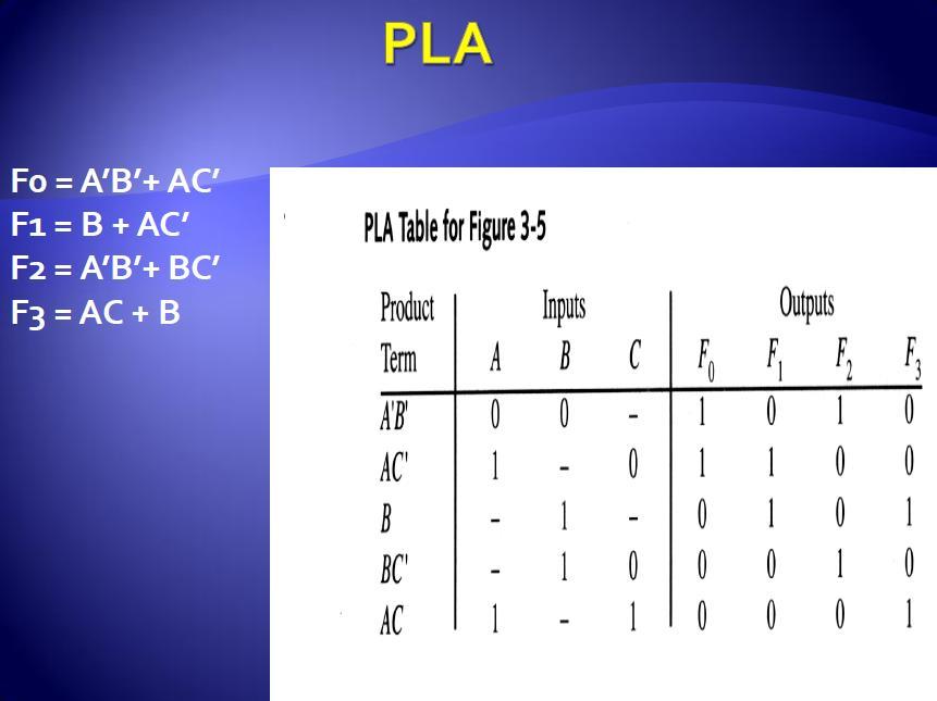
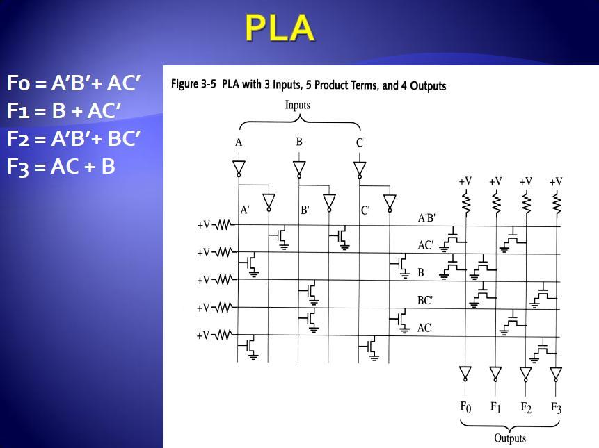
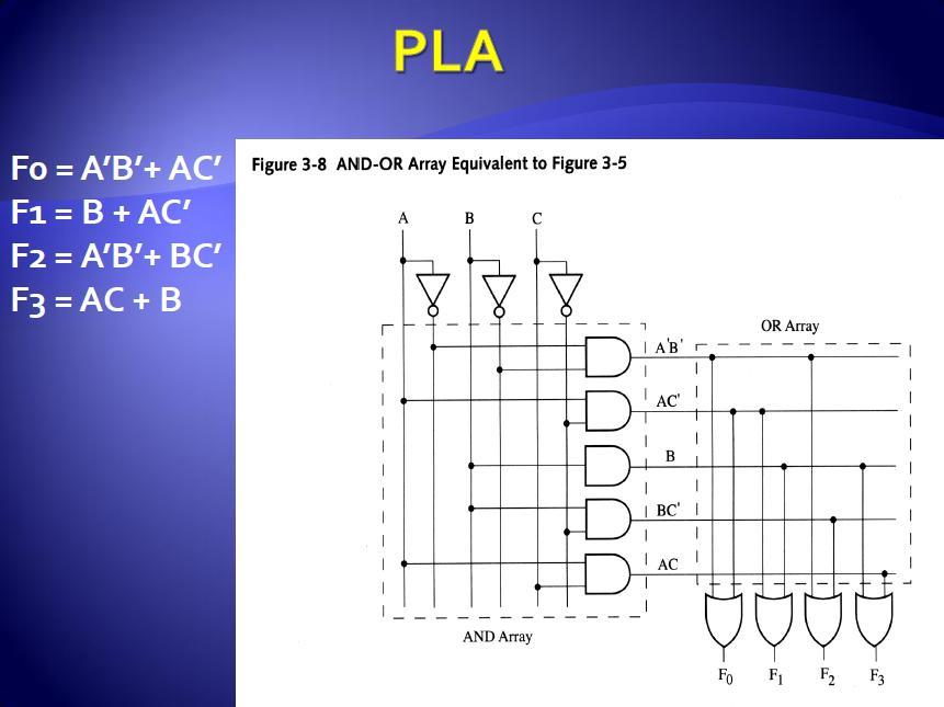
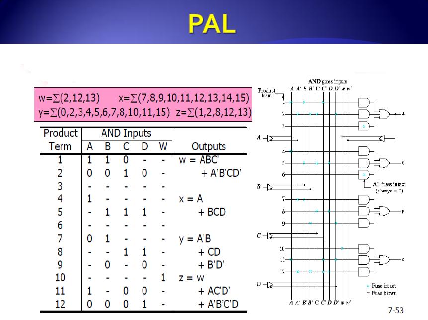
22 PAL Logic Implementation Design Example: BCD to Gray Code Converter A B Truth Table C D W X X X X X X X X X X X X X Minimized Functions: W = A + B D + B C X = B C Y = B + C Z = A B C D + B C D + A D + B C D Y X X X X X X Z X X X X X X C AB CD B A X X X X X X K-map for W A AB CD C X X X X X X B K-map for Y K-maps D D C AB CD B A X X X X X X K-map for X A AB CD C X X X X X X B K-map for Z D D 22
23 CLK D Q Q N Seq D Q Q D Seq D Q Open Reset Com 23
24 PLD (Programmable Logic Device) All layers already exist Designers can purchase an IC Connections on the IC are either created or destroyed to implement desired functionality Field-Programmable Gate Array (FPGA) very popular Benefits Low NRE costs, almost instant IC availability Drawbacks Bigger, expensive (perhaps $3 per unit), power hungry, slower Vahid & Givargis 24
25 Speed Flexibility Comparison Technology Performance/ Cost Time until running Time to high performance Time to change code functionality ASIC Very High Very Long Very Long Impossible FPGA Medium Medium Long Medium ASIP/ DSP High Long Long Long Generic Low-Medium Very Short Not Attainable Very Short 25
26 Roadmap PROM PLA PAL CPLD FPGA 26
27 PLD Definition Programmable Logic Device (PLD): An integrated circuit chip that can be configured by end use to implement different digital hardware Also known as Field Programmable Logic Device (FPLD) 27
28 PLD Advantages Short design time Nonrecurring engineering cost Less expensive at low volume PLD ASIC Volume 28
29 PLD Categorization PLD SPLD Simple PLD HCPLD High Capacity PLD PLA PAL Programmable Array Logic CPLD Complex PLD FPGA Field Programmable Gate Array 29
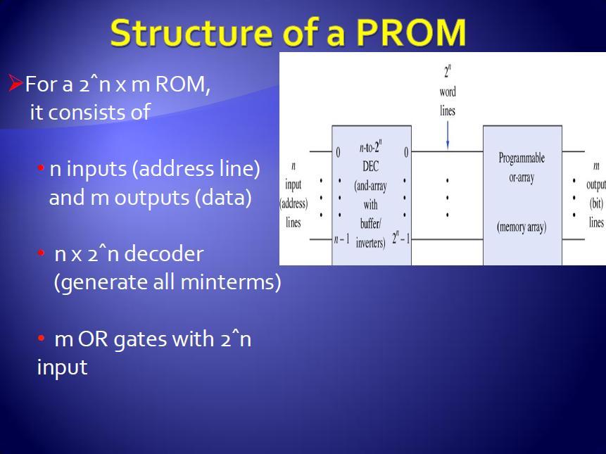
30 Programmable ROM (PROM) N input 2 N x M ROM M output Address: N bits; Output word: M bits ROM contains 2 N words of M bits each The input bits decide the particular word that becomes available on output lines 3
31 Logic Diagram of 8x3 PROM Sum of minterms 3
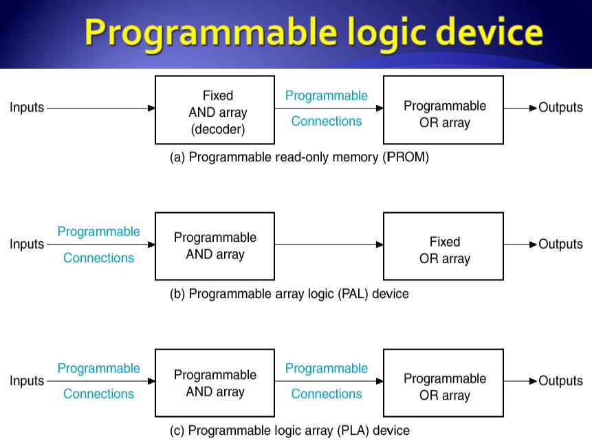
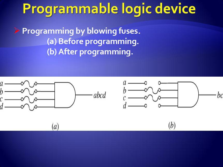
32 Combinational Circuit Implementation using PROM I I I2 F F F2 F F F2 32
33 PROM Types Programmable PROM Break links through current pulses Write once, Read multiple times Erasable PROM (EPROM) Program with ultraviolet light Write multiple times, Read multiple times Electrically Erasable PROM (EEPROM)/ Flash Memory Program with electrical signal Write multiple times, Read multiple times 33
34 PROM: Advantages and Disadvantages Widely used to implement functions with large number of inputs and outputs Design of control units (Micro-programmed control units) For combinational circuits with lots of don t care terms, PROM is a wastage of logic resources 34
35 Programmable Logic Array n x k links k AND gates k X m links m OR gates m outputs n inputs n x k links Programmable AND array + programmable OR array n x k x m PLA has 2n x k + k x m links Sum of products 35
36 PLA 4 X 6 X 2 36
37 Logic Implementation with PLA Finite number of AND gates => simplify function to minimum number of product terms Number of literals in a product term is not important since we have all the input variables Sharing of product terms between outputs => multiple-output minimization 37
38 Design with PLA 38
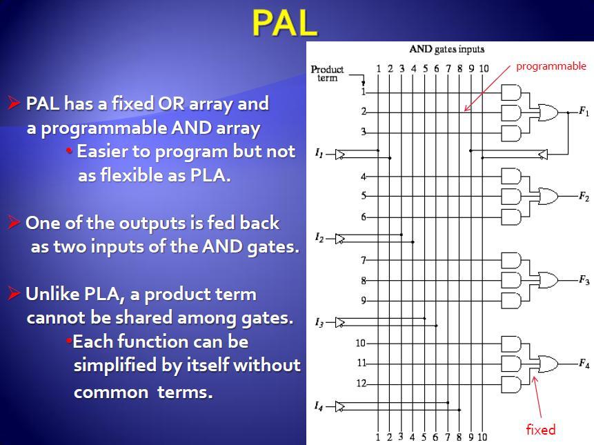
39 Programmable Array Logic (PAL) Programmable AND array Fixed OR array Each output line permanently connected to a specific set of product terms Number of switching functions that can be implemented with PAL are more limited than PROM and PLA 39
40 PAL Logic Diagram 4
41 PAL Implications Number of product terms per output > number of product terms in each sum-ofproduct expression No sharing of product terms between outputs 4
42 Design with PAL 42
43 Complex Programmable Logic Devices Complex PLDs typically combine PAL combinational logic with FFs Organized into logic blocks Fixed OR array size Combinational or registered output Some pins are inputs only Usually enough logic for simple counters, state machines, decoders, etc. e.g. GAL22V, GAL6V8, etc. 43

44 GAL CPLD OLMC (Output Logic MacroCell) has OR, FF, output multiplexer and I/O control logic. Note that OLMC output is fed back to input matrix for use in other OLMCs. 44
45 Programmable Interconnect CPLD Logic Block Logic Block I/O I/O Logic Block Logic Block 45
46 CPLD Logic Block Simple PLD Inputs Product-term array Product term allocation function Macro-cells (registers) Logic blocks executes sum-of-product expressions and stores the results in micro-cell registers Programmable interconnects route signals to and from logic blocks 46
47 Major CPLD Resources Number of macro-cells per logic block Number of inputs from programmable interconnect to logic block Number of product terms in logic block 47
48 Structure of FPGA (Xilinx) Logic Block I/O Block Interconnect 48
49 Configurable Logic Block CLB 49
50 Logic Function Implemented as look-up table (LUT) K-input LUT corresponds to 2 K x bit memory K-input LUT can implement any k-input - output logic function 5
51 Configuring FPGA Configure CLB and IOB Configure interconnect Interconnect technology SRAM Anti-fuse (program once) EPROM / EEPROM 5
52 Programming Technology Name Re-programmable Volatile EPROM yes (out of circuit) no EEPROM yes (in circuit) no SRAM yes (in circuit) yes Antifuse no no 52
53 FPGA Applications Glue Logic (replace SSI and MSI parts) Rapid turnaround Prototype design Emulation Custom computing Dynamic reconfiguration 53
Chapter 13 Programmable Logic Device Architectures
 Chapter 13 Programmable Logic Device Architectures Chapter 13 Objectives Selected areas covered in this chapter: Describing different categories of digital system devices. Describing different types of
Programmable Logic Devices
 Programmable Logic Devices INTRODUCTION A programmable logic device or PLD is an electronic component used to build reconfigurable digital circuits. Unlike a logic gate, which has a fixed function, a PLD
LSN 6 Programmable Logic Devices
 LSN 6 Programmable Logic Devices Department of Engineering Technology LSN 6 What Are PLDs? Functionless devices in base form Require programming to operate The logic function of the device is programmed
Section 6. Memory Components Chapter 5.7, 5.8 Physical Implementations Chapter 7 Programmable Processors Chapter 8
 Section 6 Memory Components Chapter 5.7, 5.8 Physical Implementations Chapter 7 Programmable Processors Chapter 8 Types of memory Two major types of memory Volatile When power to the device is removed
Embedded Controller Design. CompE 270 Digital Systems - 5. Objective. Application Specific Chips. User Programmable Logic. Copyright 1998 Ken Arnold 1
 CompE 270 Digital Systems - 5 Programmable Logic Ken Arnold Objective Application Specific ICs Introduce User Programmable Logic Common Architectures Programmable Array Logic Address Decoding Example Development
Presentation 4: Programmable Combinational Devices
 Presentation 4: Programmable Combinational Devices Asst. Prof Dr. Ahmet ÖZKURT DEUEEE Based on the Presentation by Prof. Kim, Young Ho Dept. of Information Computer Engineering E-mail : yhkim@hyowon.cs.pusan.ac.kr
Digital Integrated Circuits
 Digital Integrated Circuits Lecture 9 Jaeyong Chung Robust Systems Laboratory Incheon National University DIGITAL DESIGN FLOW Chung EPC6055 2 FPGA vs. ASIC FPGA (A programmable Logic Device) Faster time-to-market
DIGITAL SYSTEM FUNDAMENTALS (ECE421) DIGITAL ELECTRONICS FUNDAMENTAL (ECE4220. PROGRAMMABLE LOGIC DEVICES (PLDs)
 DIGITAL ELECTRONICS FUNDAMENTAL (ECE4220. PROGRAMMABLE LOGIC DEVICES (PLDs)") COURSE / CODE DIGITAL SYSTEM FUNDAMENTALS (ECE421) DIGITAL ELECTRONICS FUNDAMENTAL (ECE4220 PROGRAMMABLE LOGIC DEVICES (PLDs) A PLD, or programmable logic device, is an electronic component that is used
COURSE / CODE DIGITAL SYSTEM FUNDAMENTALS (ECE421) DIGITAL ELECTRONICS FUNDAMENTAL (ECE4220 PROGRAMMABLE LOGIC DEVICES (PLDs) A PLD, or programmable logic device, is an electronic component that is used
PROGRAMMABLE MODULES SPECIFICATION OF PROGRAMMABLE COMBINATIONAL AND SEQUENTIAL MODULES
 PROGRAMMABLE MODULES SPECIFICATION OF PROGRAMMABLE COMBINATIONAL AND SEQUENTIAL MODULES. psa. rom. fpga THE WAY THE MODULES ARE PROGRAMMED NETWORKS OF PROGRAMMABLE MODULES EXAMPLES OF USES Programmable
Evolution of Implementation Technologies. ECE 4211/5211 Rapid Prototyping with FPGAs. Gate Array Technology (IBM s) Programmable Logic
 Programmable Logic") ECE 42/52 Rapid Prototyping with FPGAs Dr. Charlie Wang Department of Electrical and Computer Engineering University of Colorado at Colorado Springs Evolution of Implementation Technologies Discrete devices:
ECE 42/52 Rapid Prototyping with FPGAs Dr. Charlie Wang Department of Electrical and Computer Engineering University of Colorado at Colorado Springs Evolution of Implementation Technologies Discrete devices:
Memory and Programmable Logic
 Memory and Programmable Logic Memory units allow us to store and/or retrieve information Essentially look-up tables Good for storing data, not for function implementation Programmable logic device (PLD),
PLAs & PALs. Programmable Logic Devices (PLDs) PLAs and PALs
 PLAs and PALs") PLAs & PALs Programmable Logic Devices (PLDs) PLAs and PALs PLAs&PALs By the late 1970s, standard logic devices were all the rage, and printed circuit boards were loaded with them. To offer the ultimate
PLAs & PALs Programmable Logic Devices (PLDs) PLAs and PALs PLAs&PALs By the late 1970s, standard logic devices were all the rage, and printed circuit boards were loaded with them. To offer the ultimate
Memory and Programmable Logic
 Digital Circuit Design and Language Memory and Programmable Logic Chang, Ik Joon Kyunghee University Memory Classification based on functionality ROM : Read-Only Memory RWM : Read-Write Memory RWM NVRWM
FPGA for Complex System Implementation. National Chiao Tung University Chun-Jen Tsai 04/14/2011
 FPGA for Complex System Implementation National Chiao Tung University Chun-Jen Tsai 04/14/2011 About FPGA FPGA was invented by Ross Freeman in 1989 SRAM-based FPGA properties Standard parts Allowing multi-level
ELCT 912: Advanced Embedded Systems
 Advanced Embedded Systems Lecture 2: Memory and Programmable Logic Dr. Mohamed Abd El Ghany, Memory Random Access Memory (RAM) Can be read and written Static Random Access Memory (SRAM) Data stored so
CHAPTER 9 MULTIPLEXERS, DECODERS, AND PROGRAMMABLE LOGIC DEVICES
 CHAPTER 9 MULTIPLEXERS, DECODERS, AND PROGRAMMABLE LOGIC DEVICES This chapter in the book includes: Objectives Study Guide 9.1 Introduction 9.2 Multiplexers 9.3 Three-State Buffers 9.4 Decoders and Encoders
PROGRAMMABLE LOGIC DEVICES
 PROGRAMMABLE LOGIC DEVICES Programmable logic devices (PLDs) are used for designing logic circuits. PLDs can be configured by the user to perform specific functions. The different types of PLDs available
Digital Electronics 27. Digital System Design using PLDs
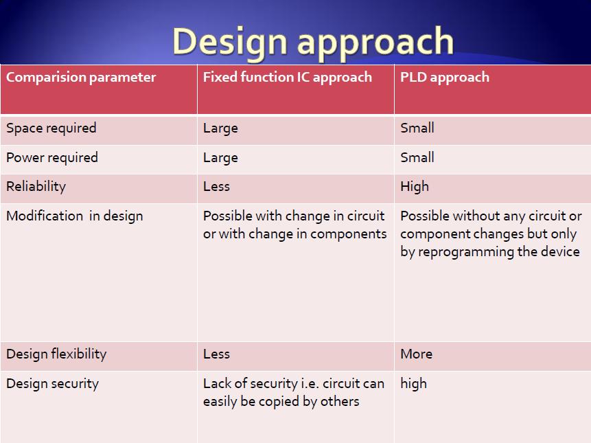
 1 Module -27 Digital System Design 1. Introduction 2. Digital System Design 2.1 Standard (Fixed function) ICs based approach 2.2 Programmable ICs based approach 3. Comparison of Digital System Design approaches
DIGITAL CIRCUIT LOGIC UNIT 9: MULTIPLEXERS, DECODERS, AND PROGRAMMABLE LOGIC DEVICES
 DIGITAL CIRCUIT LOGIC UNIT 9: MULTIPLEXERS, DECODERS, AND PROGRAMMABLE LOGIC DEVICES 1 Learning Objectives 1. Explain the function of a multiplexer. Implement a multiplexer using gates. 2. Explain the
Programmable Logic Devices
 Programmable Logic Devices Luis Entrena, Celia López, Mario García, Enrique San Millán Universidad Carlos III de Madrid Outline Tecnologies for implementing programmable circuits Simple Programmable Logic
Basic FPGA Architectures. Actel FPGAs. PLD Technologies: Antifuse. 3 Digital Systems Implementation Programmable Logic Devices
 3 Digital Systems Implementation Programmable Logic Devices Basic FPGA Architectures Why Programmable Logic Devices (PLDs)? Low cost, low risk way of implementing digital circuits as application specific
Lecture 13: Memory and Programmable Logic
 Lecture 13: Memory and Programmable Logic Syed M. Mahmud, Ph.D ECE Department Wayne State University Aby K George, ECE Department, Wayne State University Contents Introduction Random Access Memory Memory
Memory and Programmable Logic
 Memory and Programmable Logic Mano & Ciletti Chapter 7 By Suleyman TOSUN Ankara University Outline RAM Memory decoding Error detection and correction ROM Programmable Logic Array (PLA) Programmable Array
MEMORY AND PROGRAMMABLE LOGIC
 MEMORY AND PROGRAMMABLE LOGIC Memory is a device where we can store and retrieve information It can execute a read and a write Programmable Logic is a device where we can store and retrieve information
Computer Structure. Unit 2: Memory and programmable devices
 Computer Structure Unit 2: Memory and programmable devices Translated from Francisco Pérez García (fperez at us.es) by Mª Carmen Romero (mcromerot at us.es, Office G1.51, 954554324) Electronic Technology
ECE 331 Digital System Design
 ECE 331 Digital System Design Tristate Buffers, Read-Only Memories and Programmable Logic Devices (Lecture #17) The slides included herein were taken from the materials accompanying Fundamentals of Logic
FYSE420 DIGITAL ELECTRONICS. Lecture 7
 FYSE420 DIGITAL ELECTRONICS Lecture 7 1 [1] [2] [3] DIGITAL LOGIC CIRCUIT ANALYSIS & DESIGN Nelson, Nagle, Irvin, Carrol ISBN 0-13-463894-8 DIGITAL DESIGN Morris Mano Fourth edition ISBN 0-13-198924-3
Review: Chip Design Styles
 MPT-50 Introduction to omputer Design SFU, Harbour entre, Spring 007 Lecture 9: Feb. 6, 007 Programmable Logic Devices (PLDs) - Read Only Memory (ROM) - Programmable Array Logic (PAL) - Programmable Logic
EECS150 - Digital Design Lecture 6 - Field Programmable Gate Arrays (FPGAs)
") EECS150 - Digital Design Lecture 6 - Field Programmable Gate Arrays (FPGAs) September 12, 2002 John Wawrzynek Fall 2002 EECS150 - Lec06-FPGA Page 1 Outline What are FPGAs? Why use FPGAs (a short history
EECS150 - Digital Design Lecture 6 - Field Programmable Gate Arrays (FPGAs) September 12, 2002 John Wawrzynek Fall 2002 EECS150 - Lec06-FPGA Page 1 Outline What are FPGAs? Why use FPGAs (a short history
Programmable Logic Devices
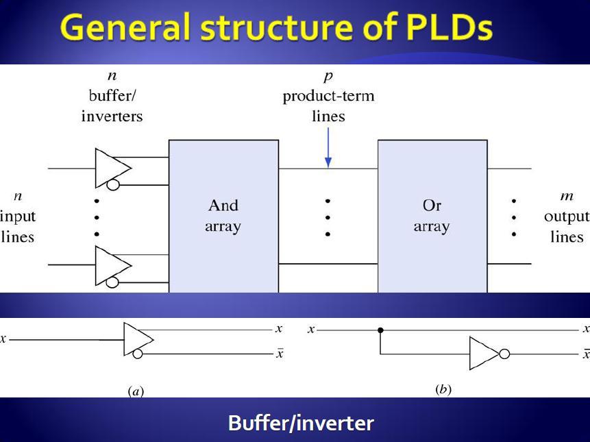
 Programmable Logic Devices Programmable Logic Devices Fig. (1) General structure of PLDs Programmable Logic Device (PLD): is an integrated circuit with internal logic gates and/or connections that can
Outline. EECS150 - Digital Design Lecture 6 - Field Programmable Gate Arrays (FPGAs) FPGA Overview. Why FPGAs?
 FPGA Overview. Why FPGAs?") EECS150 - Digital Design Lecture 6 - Field Programmable Gate Arrays (FPGAs) September 12, 2002 John Wawrzynek Outline What are FPGAs? Why use FPGAs (a short history lesson). FPGA variations Internal logic
EECS150 - Digital Design Lecture 6 - Field Programmable Gate Arrays (FPGAs) September 12, 2002 John Wawrzynek Outline What are FPGAs? Why use FPGAs (a short history lesson). FPGA variations Internal logic
ELCT 501: Digital System Design
 ELCT 501: Digital System Lecture 3: Memory and Programmable Logic (continue) Dr. Mohamed Abd El Ghany, Memory Model 32-bit address space can address up to 4 GB (2 32 ) different memory locations 0x00000000
Topics. Midterm Finish Chapter 7
 Lecture 9 Topics Midterm Finish Chapter 7 ROM (review) Memory device in which permanent binary information is stored. Example: 32 x 8 ROM Five input lines (2 5 = 32) 32 outputs, each representing a memory
Very Large Scale Integration (VLSI)
") Very Large Scale Integration (VLSI) Lecture 6 Dr. Ahmed H. Madian Ah_madian@hotmail.com Dr. Ahmed H. Madian-VLSI 1 Contents FPGA Technology Programmable logic Cell (PLC) Mux-based cells Look up table PLA
Very Large Scale Integration (VLSI) Lecture 6 Dr. Ahmed H. Madian Ah_madian@hotmail.com Dr. Ahmed H. Madian-VLSI 1 Contents FPGA Technology Programmable logic Cell (PLC) Mux-based cells Look up table PLA
Introduction to Digital Logic Missouri S&T University CPE 2210 Hardware Implementations
 Introduction to Digital Logic Missouri S&T University CPE 2210 Hardware Implementations Egemen K. Çetinkaya Egemen K. Çetinkaya Department of Electrical & Computer Engineering Missouri University of Science
Hardware Design with VHDL PLDs I ECE 443. FPGAs can be configured at least once, many are reprogrammable.
 PLDs, ASICs and FPGAs FPGA definition: Digital integrated circuit that contains configurable blocks of logic and configurable interconnects between these blocks. Key points: Manufacturer does NOT determine
Chapter 6 Selected Design Topics
 Logic and Computer Design Fundamentals Chapter 6 Selected Design Topics Part 4 Programmable Implementation Technologies Charles Kime & Thomas Kaminski 2008 Pearson Education, Inc. (Hyperlinks are active
Design Methodologies. Full-Custom Design
 Design Methodologies Design styles Full-custom design Standard-cell design Programmable logic Gate arrays and field-programmable gate arrays (FPGAs) Sea of gates System-on-a-chip (embedded cores) Design
Unit 6 1.Random Access Memory (RAM) Chapter 3 Combinational Logic Design 2.Programmable Logic
 Chapter 3 Combinational Logic Design 2.Programmable Logic") EE 200: Digital Logic Circuit Design Dr Radwan E Abdel-Aal, COE Unit 6.Random Access Memory (RAM) Chapter 3 Combinational Logic Design 2. Logic Logic and Computer Design Fundamentals Part Implementation
EE 200: Digital Logic Circuit Design Dr Radwan E Abdel-Aal, COE Unit 6.Random Access Memory (RAM) Chapter 3 Combinational Logic Design 2. Logic Logic and Computer Design Fundamentals Part Implementation
Introduction to Programmable Logic Devices (Class 7.2 2/28/2013)
") Introduction to Programmable Logic Devices (Class 7.2 2/28/2013) CSE 2441 Introduction to Digital Logic Spring 2013 Instructor Bill Carroll, Professor of CSE Today s Topics Complexity issues Implementation
Introduction to Programmable Logic Devices (Class 7.2 2/28/2013) CSE 2441 Introduction to Digital Logic Spring 2013 Instructor Bill Carroll, Professor of CSE Today s Topics Complexity issues Implementation
Model EXAM Question Bank
 VELAMMAL COLLEGE OF ENGINEERING AND TECHNOLOGY, MADURAI Department of Information Technology Model Exam -1 1. List the main difference between PLA and PAL. PLA: Both AND and OR arrays are programmable
INTRODUCTION TO FPGA ARCHITECTURE
 3/3/25 INTRODUCTION TO FPGA ARCHITECTURE DIGITAL LOGIC DESIGN (BASIC TECHNIQUES) a b a y 2input Black Box y b Functional Schematic a b y a b y a b y 2 Truth Table (AND) Truth Table (OR) Truth Table (XOR)
Programmable Logic Devices Introduction CMPE 415. Programmable Logic Devices
 Instructor: Professor Jim Plusquellic Programmable Logic Devices Text: The Design Warrior s Guide to FPGAs, Devices, Tools and Flows, Clive "Max" Maxfield, ISBN: 0-7506-7604-3 Modeling, Synthesis and Rapid
Today. Comments about assignment Max 1/T (skew = 0) Max clock skew? Comments about assignment 3 ASICs and Programmable logic Others courses
 Max clock skew? Comments about assignment 3 ASICs and Programmable logic Others courses") Today Comments about assignment 3-43 Comments about assignment 3 ASICs and Programmable logic Others courses octor Per should show up in the end of the lecture Mealy machines can not be coded in a single
Today Comments about assignment 3-43 Comments about assignment 3 ASICs and Programmable logic Others courses octor Per should show up in the end of the lecture Mealy machines can not be coded in a single
Semiconductor Memories: RAMs and ROMs
 Semiconductor Memories: RAMs and ROMs Lesson Objectives: In this lesson you will be introduced to: Different memory devices like, RAM, ROM, PROM, EPROM, EEPROM, etc. Different terms like: read, write,
UNIT - V MEMORY P.VIDYA SAGAR ( ASSOCIATE PROFESSOR) Department of Electronics and Communication Engineering, VBIT
 Department of Electronics and Communication Engineering, VBIT") UNIT - V MEMORY P.VIDYA SAGAR ( ASSOCIATE PROFESSOR) contents Memory: Introduction, Random-Access memory, Memory decoding, ROM, Programmable Logic Array, Programmable Array Logic, Sequential programmable
UNIT - V MEMORY P.VIDYA SAGAR ( ASSOCIATE PROFESSOR) contents Memory: Introduction, Random-Access memory, Memory decoding, ROM, Programmable Logic Array, Programmable Array Logic, Sequential programmable
Outline. Field Programmable Gate Arrays. Programming Technologies Architectures. Programming Interfaces. Historical perspective
 Outline Field Programmable Gate Arrays Historical perspective Programming Technologies Architectures PALs, PLDs,, and CPLDs FPGAs Programmable logic Interconnect network I/O buffers Specialized cores Programming
CMPE 415 Programmable Logic Devices FPGA Technology I
 Department of Computer Science and Electrical Engineering CMPE 415 Programmable Logic Devices FPGA Technology I Prof. Ryan Robucci Some slides (blue-frame) developed by Jim Plusquellic Some images credited
UNIT V (PROGRAMMABLE LOGIC DEVICES)
") UNIT V (PROGRAMMABLE LOGIC DEVICES) Introduction There are two types of memories that are used in digital systems: Random-access memory(ram): perform both the write and read operations. Read-only memory(rom):
UNIT V (PROGRAMMABLE LOGIC DEVICES) Introduction There are two types of memories that are used in digital systems: Random-access memory(ram): perform both the write and read operations. Read-only memory(rom):
Purdue IMPACT 2015 Edition by D. G. Meyer. Introduction to Digital System Design. Module 2 Combinational Logic Circuits
 Purdue IMPACT 25 Edition by D. G. Meyer Introduction to Digital System Design Module 2 Combinational Logic Circuits Glossary of Common Terms DISCRETE LOGIC a circuit constructed using small-scale integrated
SHRI ANGALAMMAN COLLEGE OF ENGINEERING. (An ISO 9001:2008 Certified Institution) SIRUGANOOR, TIRUCHIRAPPALLI
 SIRUGANOOR, TIRUCHIRAPPALLI") SHRI ANGALAMMAN COLLEGE OF ENGINEERING AND TECHNOLOGY (An ISO 9001:2008 Certified Institution) SIRUGANOOR, TIRUCHIRAPPALLI 621 105 DEPARTMENT OF ELECTRONICS AND COMMUNICATION ENGINEERING EC1201 DIGITAL
SHRI ANGALAMMAN COLLEGE OF ENGINEERING AND TECHNOLOGY (An ISO 9001:2008 Certified Institution) SIRUGANOOR, TIRUCHIRAPPALLI 621 105 DEPARTMENT OF ELECTRONICS AND COMMUNICATION ENGINEERING EC1201 DIGITAL
Lecture (1) Introduction to FPGA. 1. The History of Programmable Logic
 Introduction to FPGA. 1. The History of Programmable Logic") Lecture (1) Introduction to FPGA 1. The History of Programmable Logic By the late 1970s, standard logic devices were all the rage, and printed circuit boards were loaded with them. Then someone asked,
Lecture (1) Introduction to FPGA 1. The History of Programmable Logic By the late 1970s, standard logic devices were all the rage, and printed circuit boards were loaded with them. Then someone asked,
Read-only memory Implementing logic with ROM Programmable logic devices Implementing logic with PLDs Static hazards
 Points Addressed in this Lecture Lecture 7: ROM Programmable Logic Devices Professor Peter Cheung Department of EEE, Imperial College London Read-only memory Implementing logic with ROM Programmable logic
Design Methodologies and Tools. Full-Custom Design
 Design Methodologies and Tools Design styles Full-custom design Standard-cell design Programmable logic Gate arrays and field-programmable gate arrays (FPGAs) Sea of gates System-on-a-chip (embedded cores)
FPGA Implementations
 FPGA Implementations Smith Text: Chapters 4-8 Online version at: http://www10.edacafe.com/book/asic/asics.php Topic outline Chapter 4 Programmable ASIC technologies Chapter 5 Programmable logic cells Chapter
FPGA. Logic Block. Plessey FPGA: basic building block here is 2-input NAND gate which is connected to each other to implement desired function.
 FPGA Logic block of an FPGA can be configured in such a way that it can provide functionality as simple as that of transistor or as complex as that of a microprocessor. It can used to implement different
ECE 636. Reconfigurable Computing. Lecture 2. Field Programmable Gate Arrays I
 ECE 636 Reconfigurable Computing Lecture 2 Field Programmable Gate Arrays I Overview Anti-fuse and EEPROM-based devices Contemporary SRAM devices - Wiring - Embedded New trends - Single-driver wiring -
IT T35 Digital system desigm y - ii /s - iii
 UNIT - IV Sequential Logic II Memory and Programmable Logic: Random Access Memory memory decoding error detection and correction Read Only Memory Programmable Logic Arrays Programmable Array Logic. PRE-REQUISITE
FPGA for Dummies. Introduc)on to Programmable Logic
on to Programmable Logic") FPGA for Dummies Introduc)on to Programmable Logic FPGA for Dummies Historical introduc)on, where we come from; FPGA Architecture: Ø basic blocks (Logic, FFs, wires and IOs); Ø addi)onal elements; FPGA
FPGA for Dummies Introduc)on to Programmable Logic FPGA for Dummies Historical introduc)on, where we come from; FPGA Architecture: Ø basic blocks (Logic, FFs, wires and IOs); Ø addi)onal elements; FPGA
FPGA Programming Technology
 FPGA Programming Technology Static RAM: This Xilinx SRAM configuration cell is constructed from two cross-coupled inverters and uses a standard CMOS process. The configuration cell drives the gates of
Programmable Logic Devices FPGA Architectures II CMPE 415. Overview This set of notes introduces many of the features available in the FPGAs of today.
 Overview This set of notes introduces many of the features available in the FPGAs of today. The majority use SRAM based configuration cells, which allows fast reconfiguation. Allows new design ideas to
I 4 I 3 I 2 I 1 I 0 A 7 A 6 A 5 A 4 A 3 A 2 A 1 A 0 T-125. ROM Truth Table (Partial) 1997 by Prentice-Hall, Inc.
 1997 by Prentice-Hall, Inc.") 997 by Prentice-Hall, Inc. ano & Kime Upper Saddle River, New Jersey 7458 T-5 Inputs Outputs I 4 I 3 I I I A 7 A 6 A 5 A 4 A 3 A A A...... RO Truth Table (Partial) 997 by Prentice-Hall, Inc. ano & Kime
997 by Prentice-Hall, Inc. ano & Kime Upper Saddle River, New Jersey 7458 T-5 Inputs Outputs I 4 I 3 I I I A 7 A 6 A 5 A 4 A 3 A A A...... RO Truth Table (Partial) 997 by Prentice-Hall, Inc. ano & Kime
Programmable Logic Devices. Programmable Read Only Memory (PROM) Example
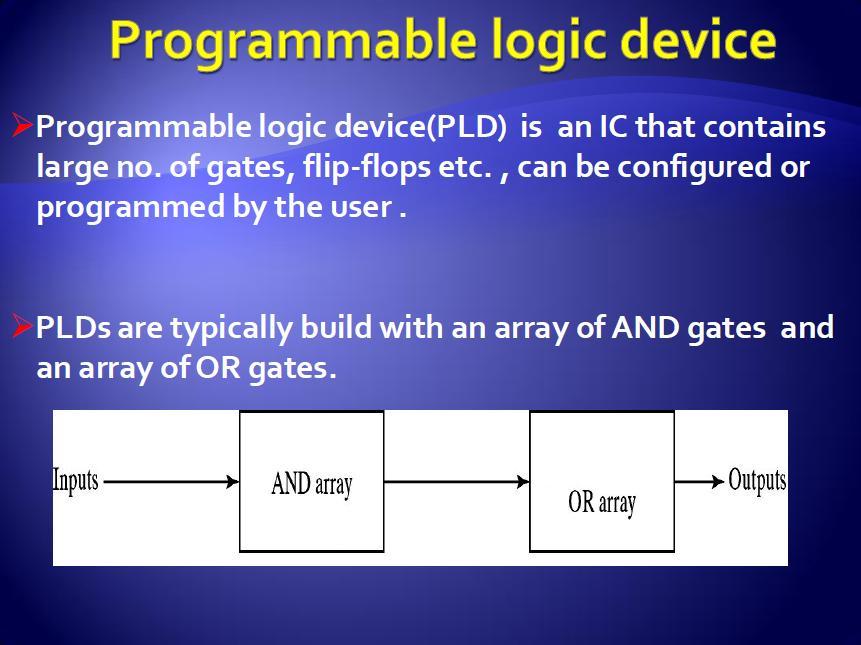
 Example") Programmable Logic Devices Programmable Logic Devices (PLDs) are the integrated circuits. They contain an array of AND gates & another array of OR gates. There are three kinds of PLDs based on the type
Programmable Logic Devices Programmable Logic Devices (PLDs) are the integrated circuits. They contain an array of AND gates & another array of OR gates. There are three kinds of PLDs based on the type
VALLIAMMAI ENGINEERING COLLEGE. SRM Nagar, Kattankulathur DEPARTMENT OF ELECTRONICS AND COMMUNICATION ENGINEERING EC6302 DIGITAL ELECTRONICS
 VALLIAMMAI ENGINEERING COLLEGE SRM Nagar, Kattankulathur-603 203 DEPARTMENT OF ELECTRONICS AND COMMUNICATION ENGINEERING EC6302 DIGITAL ELECTRONICS YEAR / SEMESTER: II / III ACADEMIC YEAR: 2015-2016 (ODD
FPGA: What? Why? Marco D. Santambrogio
 FPGA: What? Why? Marco D. Santambrogio marco.santambrogio@polimi.it 2 Reconfigurable Hardware Reconfigurable computing is intended to fill the gap between hardware and software, achieving potentially much
Programmable Logic Devices (PLDs)
") Programmable Logic Devices (PLDs) 212: Digital Design I, week 13 PLDs basically store binary information in a volatile/nonvolatile device. Data is specified by designer and physically inserted (Programmed)
Programmable Logic Devices (PLDs) 212: Digital Design I, week 13 PLDs basically store binary information in a volatile/nonvolatile device. Data is specified by designer and physically inserted (Programmed)
Sistemas Digitais I LESI - 2º ano
 Sistemas Digitais I LESI - 2º ano Lesson 9 - Memory, CPLDs and FPGAs Prof. João Miguel Fernandes (miguel@di.uminho.pt) Dept. Informática UNIVERSIDADE DO MINHO ESCOLA DE ENGENHARIA - Memory - Any sequential
PALs, GALs & CUPL. What is Programmable Logic?
 PALs, GALs & CUPL A lesson on Programmable Logic Devices and programming them using CUPL What is Programmable Logic? Digital integrated circuits where the Boolean function can be determined by the user.
L2: FPGA HARDWARE : ADVANCED DIGITAL DESIGN PROJECT FALL 2015 BRANDON LUCIA
 L2: FPGA HARDWARE 18-545: ADVANCED DIGITAL DESIGN PROJECT FALL 2015 BRANDON LUCIA 18-545: FALL 2014 2 Admin stuff Project Proposals happen on Monday Be prepared to give an in-class presentation Lab 1 is
Fig. 6-1 Conventional and Array Logic Symbols for OR Gate
 6- (a) Conventional symbol (b) Array logic symbol Fig. 6- Conventional and Array Logic Symbols for OR Gate 2 Prentice Hall, Inc. 6-2 k address lines Read n data input lines emory unit 2 k words n bits
8051 INTERFACING TO EXTERNAL MEMORY
 8051 INTERFACING TO EXTERNAL MEMORY Memory Capacity The number of bits that a semiconductor memory chip can store Called chip capacity It can be in units of Kbits (kilobits), Mbits (megabits), and so on
Field Program mable Gate Arrays
 Field Program mable Gate Arrays M andakini Patil E H E P g r o u p D H E P T I F R SERC school NISER, Bhubaneshwar Nov 7-27 2017 Outline Digital electronics Short history of programmable logic devices
EECS 150 Homework 7 Solutions Fall (a) 4.3 The functions for the 7 segment display decoder given in Section 4.3 are:
 4.3 The functions for the 7 segment display decoder given in Section 4.3 are:") Problem 1: CLD2 Problems. (a) 4.3 The functions for the 7 segment display decoder given in Section 4.3 are: C 0 = A + BD + C + BD C 1 = A + CD + CD + B C 2 = A + B + C + D C 3 = BD + CD + BCD + BC C 4
Problem 1: CLD2 Problems. (a) 4.3 The functions for the 7 segment display decoder given in Section 4.3 are: C 0 = A + BD + C + BD C 1 = A + CD + CD + B C 2 = A + B + C + D C 3 = BD + CD + BCD + BC C 4
Getting Embedded Software into the Target System using Device Programmer
 Embedded Software development Process and Tools: Lesson-5 Getting Embedded Software into the Target System using Device Programmer 1 1. Device PROM or Flash Programmer 2 Device programmer also called laboratory
Programmable Logic Devices I. EECE143 Lecture 4. PALs, GALs & CUPL. A lesson on Programmable Logic Devices and programming them using CUPL
 PALs, GALs & CUPL A lesson on Programmable Logic Devices and programming them using CUPL What is Programmable Logic? Digital integrated circuits where the Boolean function can be determined by the user.
CS310 Embedded Computer Systems. Maeng
 1 INTRODUCTION (PART II) Maeng Three key embedded system technologies 2 Technology A manner of accomplishing a task, especially using technical processes, methods, or knowledge Three key technologies for
Introduction PLD - Programmable Logic Device Hardware focus typically on Microprocessor, microcontroller, and microcomputer
 Programmable Logic Devices Overview In this lesson we will Begin with an overview of programmable logic devices - PLDs. Motivate the use of PLDs. Introduce some of the basic underlying concepts in PLDs.
SECTION-A
 M.Sc(CS) ( First Semester) Examination,2013 Digital Electronics Paper: Fifth ------------------------------------------------------------------------------------- SECTION-A I) An electronics circuit/ device
Chapter 5: ASICs Vs. PLDs
 Chapter 5: ASICs Vs. PLDs 5.1 Introduction A general definition of the term Application Specific Integrated Circuit (ASIC) is virtually every type of chip that is designed to perform a dedicated task.
Programmable Logic. Any other approaches?
 Programmable Logic So far, have only talked about PALs (see 22V10 figure next page). What is the next step in the evolution of PLDs? More gates! How do we get more gates? We could put several PALs on one
Electronic Control systems are also: Members of the Mechatronic Systems. Control System Implementation. Printed Circuit Boards (PCBs) - #1
 - #1") Control System Implementation Hardware implementation Electronic Control systems are also: Members of the Mechatronic Systems Concurrent design (Top-down approach?) Mechanic compatibility Solve the actual
Control System Implementation Hardware implementation Electronic Control systems are also: Members of the Mechatronic Systems Concurrent design (Top-down approach?) Mechanic compatibility Solve the actual
Follow-up question: now, comment on what each of these acronyms actually means, going beyond a mere recitation of the definition.
 Question 1 Define the following acronyms as they apply to digital logic circuits: ASIC PAL PLA PLD CPLD FPGA file 03041 Answer 1 ASIC: Application-Specific Integrated Circuit PAL: Programmable Array Logic
INTERNATIONAL JOURNAL OF PURE AND APPLIED RESEARCH IN ENGINEERING AND TECHNOLOGY
 INTERNATIONAL JOURNAL OF PURE AND APPLIED RESEARCH IN ENGINEERING AND TECHNOLOGY A PATH FOR HORIZING YOUR INNOVATIVE WORK FIELD PROGRAMMABLE GATE ARRAY MS. HITAISHEE V. DESHMUKH Department of Electronics
Control System Implementation
 Control System Implementation Hardware implementation Electronic Control systems are also: Members of the Mechatronic Systems Concurrent design (Top-down approach?) Mechanic compatibility Solve the actual
Concept of Memory. The memory of computer is broadly categories into two categories:
 Concept of Memory We have already mentioned that digital computer works on stored programmed concept introduced by Von Neumann. We use memory to store the information, which includes both program and data.
MGU-BCA-205- Second Sem- Core VI- Fundamentals of Digital Systems- MCQ s. 2. Why the decimal number system is also called as positional number system?
 MGU-BCA-205- Second Sem- Core VI- Fundamentals of Digital Systems- MCQ s Unit-1 Number Systems 1. What does a decimal number represents? A. Quality B. Quantity C. Position D. None of the above 2. Why the
Field Programmable Gate Array (FPGA)
") Field Programmable Gate Array (FPGA) Lecturer: Krébesz, Tamas 1 FPGA in general Reprogrammable Si chip Invented in 1985 by Ross Freeman (Xilinx inc.) Combines the advantages of ASIC and uc-based systems
Field Programmable Gate Array (FPGA) Lecturer: Krébesz, Tamas 1 FPGA in general Reprogrammable Si chip Invented in 1985 by Ross Freeman (Xilinx inc.) Combines the advantages of ASIC and uc-based systems
Injntu.com Injntu.com Injntu.com R16
 1. a) What are the three methods of obtaining the 2 s complement of a given binary (3M) number? b) What do you mean by K-map? Name it advantages and disadvantages. (3M) c) Distinguish between a half-adder
Review. EECS Components and Design Techniques for Digital Systems. Lec 03 Field Programmable Gate Arrays
 EECS 5 - Components and Design Techniques for Digital Systems Lec 3 Field Programmable Gate Arrays 9-4-7 David Culler Electrical Engineering and Computer Sciences University of California, Berkeley http://www.eecs.berkeley.edu/~culler
Programmable logic technology
 Programmable logic technology This worksheet and all related files are licensed under the Creative Commons Attribution License, version 1.0. To view a copy of this license, visit http://creativecommons.org/licenses/by/1.0/,
FPGA Based Digital Design Using Verilog HDL
 FPGA Based Digital Design Using Course Designed by: IRFAN FAISAL MIR ( Verilog / FPGA Designer ) irfanfaisalmir@yahoo.com * Organized by Electronics Division Integrated Circuits Uses for digital IC technology
Chapter 10: Design Options of Digital Systems
 Chapter 10: Design Options of Digital Systems Prof. Ming-Bo Lin Department of Electronic Engineering National Taiwan University of Science and Technology Digital System Designs and Practices Using Verilog
CPLDs vs. FPGAs: Comparing High-Capacity Programmable Logic
 PIB 18 CPLDs vs. FPGAs: Comparing High-Capacity Programmable Logic CPLDs vs. FPGAs Comparing High-Capacity Programmable Logic February 1995, ver. 1 Product Information Bulletin 18 Introduction The high-capacity
EE178 Lecture Module 2. Eric Crabill SJSU / Xilinx Fall 2007
 EE178 Lecture Module 2 Eric Crabill SJSU / Xilinx Fall 2007 Lecture #4 Agenda Survey of implementation technologies. Implementation Technologies Small scale and medium scale integration. Up to about 200
CSEE 3827: Fundamentals of Computer Systems. Storage
 CSEE 387: Fundamentals of Computer Systems Storage The big picture General purpose processor (e.g., Power PC, Pentium, MIPS) Internet router (intrusion detection, pacet routing, etc.) WIreless transceiver
Lecture (05) Boolean Algebra and Logic Gates
 Boolean Algebra and Logic Gates") Lecture (05) Boolean Algebra and Logic Gates By: Dr. Ahmed ElShafee ١ Minterms and Maxterms consider two binary variables x and y combined with an AND operation. Since eachv ariable may appear in either
Lecture (05) Boolean Algebra and Logic Gates By: Dr. Ahmed ElShafee ١ Minterms and Maxterms consider two binary variables x and y combined with an AND operation. Since eachv ariable may appear in either
SPLD & CPLD architectures
 Module: Electronics & Telecomunication, 5rd year Hardware Acceleration of Telecommunication Protocols SPLD & CPLD architectures 1 PLD devices classification Source: Dataquest Logic Standard Logic ASIC
Code No: 07A3EC03 Set No. 1
 Code No: 07A3EC03 Set No. 1 II B.Tech I Semester Regular Examinations, November 2008 SWITCHING THEORY AND LOGIC DESIGN ( Common to Electrical & Electronic Engineering, Electronics & Instrumentation Engineering,
Microcontroller Systems. ELET 3232 Topic 11: General Memory Interfacing
 Microcontroller Systems ELET 3232 Topic 11: General Memory Interfacing 1 Objectives To become familiar with the concepts of memory expansion and the data and address bus To design embedded systems circuits
BHARATHIDASAN ENGINEERING COLLEGE Degree / Branch : B.E./ECE Year / Sem : II/ III Sub.Code / Name : EC6302/DIGITAL ELECTRONICS
 BHARATHIDASAN ENGINEERING COLLEGE Degree / Branch : B.E./ECE Year / Sem : II/ III Sub.Code / Name : EC6302/DIGITAL ELECTRONICS FREQUENTLY ASKED QUESTIONS UNIT I MINIMIZATION TECHNIQUES AND LOGIC GATES