Lab #12: ArithmeticLogic Unit
|
|
|
- Arabella Russell
- 6 years ago
- Views:
Transcription
1 Lab #12: ArithmeticLogic Unit Zack Mattis Lab: 3/27/17 Report: 4/8/17 Partner: Brendan Schuster
2 Purpose In this lab, a fully functioning 4-bit Arithmetic Logic Unit (ALU) was designed and fully implemented onto a protoboard that is capable of performing a number of operations. ALUs can perform both arithmetic operations such as addition and subtraction as well as logical operations including ANDs and ORs. ALUs are utilized by CPUs to provide the data calculations of the specified functions. This implementation utilizes a 4 x 4 register previously created and a 4-bit latch to provide the inputs to the ALU. Additionally, the output of the ALU is fed back into the 4 x 4 register through the use of a 4 x 2:1 MUX to store the calculated hexadecimal values in the registers. Two 7-segment displays are included to observe the output of the ALU as well as the output value of the 4 x 4 register. The design can be seen in Figure 1 below. The operation of the design was verified using the LogicPort Logic Analyzer to observe the signals of the circuit. The design was implemented using one 4x4 register (74LS670), one ALU (74LS181), two counters (74LS193), one 4 x 2:1 MUX (74LS157), two D Flip-Flops (74LS74), two 7-segment display drivers/decoders (74LS247), two 7segment displays, three 8-bit DIP SPST switches, one SPST switch, 18 resistors, and 4 LEDs. Figure 1 4 bit ALU
3 Procedure The design for the 4-bit ALU was created using the Altera Quartus 9.1 software and can be seen in Figure 2 (see attached). The design uses a 4x4 register combined with 2 counters for the read/write, and 4-bit latch, a 4-bit ALU, and two decoders for the seven segment displays that convert the hexadecimal input/output into a visual 7 segment output display. Additionally, a 4 x 2:1 MUX supplies the input of the 4 x 4 register from either user-selected input data or the output of the ALU to store the calculated data in the registers. This design was then tested using the Quartus simulation tool that allows for user selected data for each of the inputs. By manipulating the data in the 4 x 4 register, and sending it to the latch, the user can select the two data operands of the ALU. By changing the select lines of the ALU (S[3] S[0]), the mode (M), and the carry in (Cin), the user can select which ALU operation he/she wishes to perform. Four different operations (addition, subtraction, AND, OR) were tested using Quartus and their respective waveforms can be seen in Figures 3-6 (see attached). Finally, 4 hexadecimal digits were added together using the 4 registers of the 4x4 register. The values 1, 2, 2, and 3 were added to get the final output of 8, which can be seen in Figure 7 (see attached). The verified design was then implemented onto the protoboard using the previously mentioned IC chips. DIP switches were used to provide the control signals as well as the 4-bit data signals. A SPST switch was used to provide the clocking signal for the latch to store the 4-bit hex value from the register. The ALU inputs were from the 4-bit latch and from the 4x4 register. Through the use of the 4 x 2:1 MUX, the output of the ALU was wired back into the register so that it could be stored. Both the register value and the output from the ALU were wired to seven-segment display decoders and then seven segment displays. These displays allowed for easy viewing of the hexadecimal value that was being produced. Additionally, LEDs were added to the output of each counter to view which register was active. This protoboard implementation was then analyzed using the LogicPort Logic Analyzer. This device converts the analog signal of the circuit into a digital form of 0s and 1s. This tool enables effective observation of the circuit s inputs and outputs. In our testing, we connected the device to 19 data inputs. Each of the four operations simulated in Quartus were then tested on the Logic Analyzer. The output waveforms of addition, subtraction, AND, and OR can be seen Figures 8-11 (see attached), respectively.

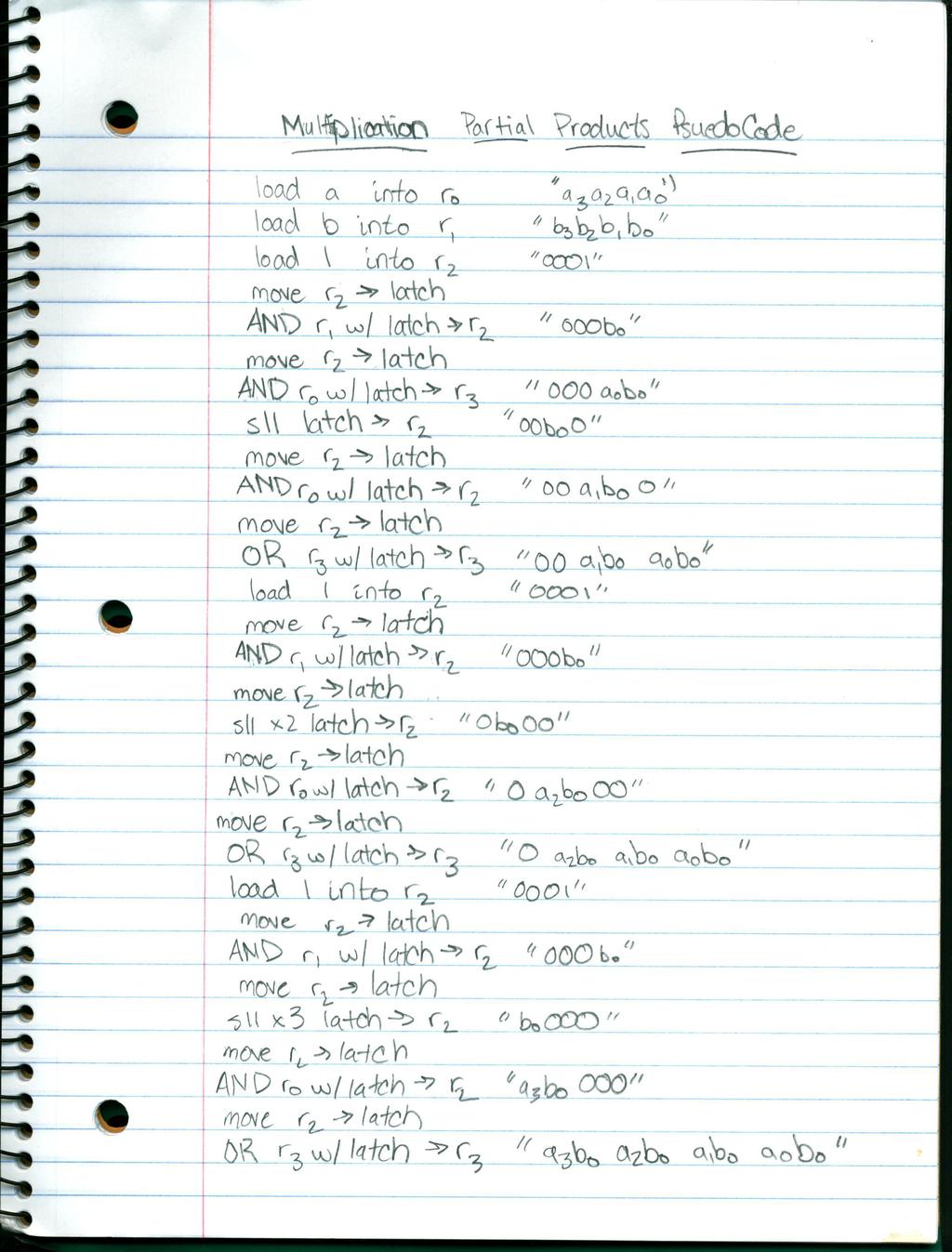
4 Results The use of a 4x4 register wired in combination with a 4-bit latch allows for effective input signals for the operands of the ALU. Utilization of a 4 x 2:1 MUX was a necessary implementation for the ALU in order to store the calculated data output in the register. Additionally, the use of seven segment displays allowed the user to easily see the hexadecimal value stored within the register as well as the hexadecimal output of the ALU. The use of LEDs for the output of the counter also allow the user to see which register has been selected. Our completed circuit design can be seen in Figure 12 below. Using this completed ALU protoboard implementation, we were able to implement a 4-bit multiplication operation using the pseudocode shown in Figure 13 (see attached). This pseudocode is used to find the first partial product (a3b0 a2b0 a1b0 a0b0) of the multiplication of operands A (a3a2a1a0) & B (b3b2b1b0). This multiplication was then analyzed using the Logic Analyzer to verify its operation. The multiplication waveform can be seen in Figure 14 (see attached). Figure 12 ALU Protoboard Implementation
5 Conclusion The design implementation of the 4-bit ALU from Figure 2 proved to be a successful design. This protoboard circuit works as a fully-functional ALU capable of performing all of the operations required from a CPU. The LogicPort Logic Analyzer output waveforms from Figures 8-11 shows the user correctly utilizing the ALU to perform both arithmetic and logical operations (addition, subtraction, AND, OR). Without a multiplication operation integrated within the ALU, utilization of the pseudocode shown in Figure 13 using AND, OR, shift, & addition operations can be used to calculate partial products to store within registers to calculate a final 4-bit hexadecimal product. The ALU design and implementation was a practical application to understanding how the CPUs of computers utilize ALUs to provide the operations necessary to function properly. References 1. ECE 0501 Digital Systems Laboratory Custom Course Materials. Laboratory Notebook. University of Pittsburgh.
6
7
8
9
10
11
12
13
14
15
16
17
EXPERIMENT NUMBER 11 REGISTERED ALU DESIGN
 11-1 EXPERIMENT NUMBER 11 REGISTERED ALU DESIGN Purpose Extend the design of the basic four bit adder to include other arithmetic and logic functions. References Wakerly: Section 5.1 Materials Required
ENEE 245 Lab 1 Report Rubrics
 ENEE 4 Lab 1 Report Rubrics Design Clearly state the design requirements Derive the minimum SOP Show the circuit implementation. Draw logic diagram and wiring diagram neatly Label all the diagrams/tables
The Itanium Bit Microprocessor Report
 The Itanium - 1986 8 Bit Microprocessor Report By PRIYANK JAIN (02010123) Group # 11 Under guidance of Dr. J. K. Deka & Dr. S. B. Nair Department of Computer Science & Engineering Indian Institute of Technology,
Laboratory 10. Programming a PIC Microcontroller - Part II
 Laboratory 10 Programming a PIC Microcontroller - Part II Required Components: 1 PIC16F88 18P-DIP microcontroller 1 0.1 F capacitor 3 SPST microswitches or NO buttons 4 1k resistors 1 MAN 6910 or LTD-482EC
Chapter 2 Logic Gates and Introduction to Computer Architecture
 Chapter 2 Logic Gates and Introduction to Computer Architecture 2.1 Introduction The basic components of an Integrated Circuit (IC) is logic gates which made of transistors, in digital system there are
Laboratory 4 Design a Muti-bit Counter
 Laboratory 4 Design a Muti-bit Counter Background A. Approach I: Design 3-bit counter with and clear T-type flip-flop is shown in Figure 1. A T flip-flop is obtained from a JK flip-flop by tying the J
Laboratory Exercise 3
 Laboratory Exercise 3 Latches, Flip-flops, and egisters The purpose of this exercise is to investigate latches, flip-flops, and registers. Part I Altera FPGAs include flip-flops that are available for
REGISTER TRANSFER LANGUAGE
 REGISTER TRANSFER LANGUAGE The operations executed on the data stored in the registers are called micro operations. Classifications of micro operations Register transfer micro operations Arithmetic micro
Laboratory 4 Design a Muti-bit Counter and Programming a FPGA
 Laboratory 4 Design a Muti-bit Counter and Programming a FPGA For your report: The problem written in English The flowchart or function table to solve the problem if it is necessary The design entry included
Lab 3: Standard Combinational Components
 Lab 3: Standard Combinational Components Purpose In this lab you will implement several combinational circuits on the DE1 development board to test and verify their operations. Introduction Using a high-level
For Example: P: LOAD 5 R0. The command given here is used to load a data 5 to the register R0.
 Register Transfer Language Computers are the electronic devices which have several sets of digital hardware which are inter connected to exchange data. Digital hardware comprises of VLSI Chips which are
Memory Supplement for Section 3.6 of the textbook
 The most basic -bit memory is the SR-latch with consists of two cross-coupled NOR gates. R Recall the NOR gate truth table: A S B (A + B) The S stands for Set to remember, and the R for Reset to remember.
IA Digital Electronics - Supervision I
 IA Digital Electronics - Supervision I Nandor Licker Due noon two days before the supervision 1 Overview The goal of this exercise is to design an 8-digit calculator capable of adding
To design a 4-bit ALU To experimentally check the operation of the ALU
 1 Experiment # 11 Design and Implementation of a 4 - bit ALU Objectives: The objectives of this lab are: To design a 4-bit ALU To experimentally check the operation of the ALU Overview An Arithmetic Logic
EET 1131 Lab #7 Arithmetic Circuits
 Name Equipment and Components Safety glasses ETS-7000 Digital-Analog Training System Integrated Circuits: 7483, 74181 Quartus II software and Altera DE2-115 board Multisim simulation software EET 1131
Register Transfer and Micro-operations
 Register Transfer Language Register Transfer Bus Memory Transfer Micro-operations Some Application of Logic Micro Operations Register Transfer and Micro-operations Learning Objectives After reading this
ENEE245 Digital Circuits and Systems Lab Manual
 ENEE245 Digital Circuits and Systems Lab Manual Department of Engineering, Physical & Computer Sciences Montgomery College Version 1.1 Copyright Prof. Lan Xiang (Do not distribute without permission) 1
Scheme G. Sample Test Paper-I
 Sample Test Paper-I Marks : 25 Times:1 Hour 1. All questions are compulsory. 2. Illustrate your answers with neat sketches wherever necessary. 3. Figures to the right indicate full marks. 4. Assume suitable
ENEE245 Digital Circuits and Systems Lab Manual
 ENEE245 Digital Circuits and Systems Lab Manual Department of Engineering, Physical & Computer Sciences Montgomery College Modified Fall 2017 Copyright Prof. Lan Xiang (Do not distribute without permission)
EE577A FINAL PROJECT REPORT Design of a General Purpose CPU
 EE577A FINAL PROJECT REPORT Design of a General Purpose CPU Submitted By Youngseok Lee - 4930239194 Narayana Reddy Lekkala - 9623274062 Chirag Ahuja - 5920609598 Phase 2 Part 1 A. Introduction The core
EE 231 Fall Lab 2: Decoders and Multiplexers. Introduction
 Lab 2: Decoders and Multiplexers Introduction Decoders and multiplexers are important combinational circuits in many logic designs. Decoders convert n inputs to a maximum of unique 2 n outputs. A special
Computer architecture Assignment 3
 Computer architecture Assignment 3 1- An instruction at address 14E in the basic computer has I=0, an operation code of the AND instruction, and an address part equal to 109(all numbers are in hexadecimal).
Digital Design with FPGAs. By Neeraj Kulkarni
 Digital Design with FPGAs By Neeraj Kulkarni Some Basic Electronics Basic Elements: Gates: And, Or, Nor, Nand, Xor.. Memory elements: Flip Flops, Registers.. Techniques to design a circuit using basic
UNIT-III REGISTER TRANSFER LANGUAGE AND DESIGN OF CONTROL UNIT
 UNIT-III 1 KNREDDY UNIT-III REGISTER TRANSFER LANGUAGE AND DESIGN OF CONTROL UNIT Register Transfer: Register Transfer Language Register Transfer Bus and Memory Transfers Arithmetic Micro operations Logic
Rensselaer Polytechnic Institute Computer Hardware Design ECSE Lab Assignment 3 Altera Richards Controller and Logic Analyzer Laboratory Rev.
 RPI Rensselaer Polytechnic Institute Computer Hardware Design ECSE 4770 Lab Assignment 3 Altera Richards Controller and Logic Analyzer Laboratory Rev.F Introduction This laboratory assignment is an introduction
LABORATORY MANUAL VLSI DESIGN LAB EE-330-F
 LABORATORY MANUAL VLSI DESIGN LAB EE-330-F (VI th Semester) Prepared By: Vikrant Verma B. Tech. (ECE), M. Tech. (ECE) Department of Electrical & Electronics Engineering BRCM College of Engineering & Technology
Dec Hex Bin ORG ; ZERO. Introduction To Computing
 Dec Hex Bin 0 0 00000000 ORG ; ZERO Introduction To Computing OBJECTIVES this chapter enables the student to: Convert any number from base 2, base 10, or base 16 to any of the other two bases. Add and
CSCB58 - Lab 3. Prelab /3 Part I (in-lab) /2 Part II (in-lab) /2 TOTAL /8
 /2 Part II (in-lab) /2 TOTAL /8") CSCB58 - Lab 3 Latches, Flip-flops, and Registers Learning Objectives The purpose of this exercise is to investigate the fundamental synchronous logic elements: latches, flip-flops, and registers. Prelab
CSCB58 - Lab 3 Latches, Flip-flops, and Registers Learning Objectives The purpose of this exercise is to investigate the fundamental synchronous logic elements: latches, flip-flops, and registers. Prelab
BUILDING BLOCKS OF A BASIC MICROPROCESSOR. Part 1 PowerPoint Format of Lecture 3 of Book
 BUILDING BLOCKS OF A BASIC MICROPROCESSOR Part PowerPoint Format of Lecture 3 of Book Decoder Tri-state device Full adder, full subtractor Arithmetic Logic Unit (ALU) Memories Example showing how to write
The Processor: Datapath and Control. Jin-Soo Kim Computer Systems Laboratory Sungkyunkwan University
 The Processor: Datapath and Control Jin-Soo Kim (jinsookim@skku.edu) Computer Systems Laboratory Sungkyunkwan University http://csl.skku.edu Introduction CPU performance factors Instruction count Determined
Lab 6: Integrated the Decoder with Muti-bit Counter and Programming a FPGA
 Lab 6: Integrated the Decoder with Muti-bit Counter and Programming a FPGA For your report: The problem written in English The flowchart or function table to solve the problem if it is necessary The design
Chapter 5. Computer Architecture Organization and Design. Computer System Architecture Database Lab, SANGJI University
 Chapter 5. Computer Architecture Organization and Design Computer System Architecture Database Lab, SANGJI University Computer Architecture Organization and Design Instruction Codes Computer Registers
Announcements. This week: no lab, no quiz, just midterm
 CSC258 Week 7 Announcements This week: no lab, no quiz, just midterm 2 Recap ALU Multiplication 3 To implement multiplication, we basically repeatedly do three things AND (one-bit multiplication) Addition
Chapter 4. The Processor
 Chapter 4 The Processor Introduction CPU performance factors Instruction count Determined by ISA and compiler CPI and Cycle time Determined by CPU hardware 4.1 Introduction We will examine two MIPS implementations
MICROPROCESSOR B.Tech. th ECE
 MICROPROCESSOR B.Tech. th ECE Submitted by: Er. Amita Sharma Dept. of ECE 11/24/2014 2 Microprocessor Architecture The microprocessor can be programmed to perform functions on given data by writing specific
Control Unit: The control unit provides the necessary timing and control Microprocessor resembles a CPU exactly.
 Unit I 8085 and 8086 PROCESSOR Introduction to microprocessor A microprocessor is a clock-driven semiconductor device consisting of electronic logic circuits manufactured by using either a large-scale
Chapter 1. Microprocessor architecture ECE Dr. Mohamed Mahmoud.
 Chapter 1 Microprocessor architecture ECE 3130 Dr. Mohamed Mahmoud The slides are copyright protected. It is not permissible to use them without a permission from Dr Mahmoud http://www.cae.tntech.edu/~mmahmoud/
Rensselaer Polytechnic Institute Computer Hardware Design ECSE 4770
 RPI Rensselaer Polytechnic Institute Computer Hardware Design ECSE 4770 Lab Assignment 2 Protoboard Richards Controller and Logic Analyzer Laboratory Rev. C Introduction This laboratory assignment is an
Chapter 4. The Processor. Instruction count Determined by ISA and compiler. We will examine two MIPS implementations
 Chapter 4 The Processor Part I Introduction CPU performance factors Instruction count Determined by ISA and compiler CPI and Cycle time Determined by CPU hardware We will examine two MIPS implementations
CS 31: Intro to Systems Digital Logic. Kevin Webb Swarthmore College February 3, 2015
 CS 31: Intro to Systems Digital Logic Kevin Webb Swarthmore College February 3, 2015 Reading Quiz Today Hardware basics Machine memory models Digital signals Logic gates Circuits: Borrow some paper if
EE 3170 Microcontroller Applications
 EE 3170 Microcontroller Applications Lecture 4 : Processors, Computers, and Controllers - 1.2 (reading assignment), 1.3-1.5 Based on slides for ECE3170 by Profs. Kieckhafer, Davis, Tan, and Cischke Outline
CS 31: Intro to Systems Digital Logic. Kevin Webb Swarthmore College February 2, 2016
 CS 31: Intro to Systems Digital Logic Kevin Webb Swarthmore College February 2, 2016 Reading Quiz Today Hardware basics Machine memory models Digital signals Logic gates Circuits: Borrow some paper if
Chapter 4. The Processor
 Chapter 4 The Processor Introduction CPU performance factors Instruction count Determined by ISA and compiler CPI and Cycle time Determined by CPU hardware We will examine two MIPS implementations A simplified
Code No: R Set No. 1
 Code No: R059210504 Set No. 1 II B.Tech I Semester Regular Examinations, November 2007 DIGITAL LOGIC DESIGN ( Common to Computer Science & Engineering, Information Technology and Computer Science & Systems
Institute of Engineering & Management
 Course:CS493- Computer Architecture Lab PROGRAMME: COMPUTERSCIENCE&ENGINEERING DEGREE:B. TECH COURSE: Computer Architecture Lab SEMESTER: 4 CREDITS: 2 COURSECODE: CS493 COURSE TYPE: Practical COURSE AREA/DOMAIN:
CSE 141L Computer Architecture Lab Fall Lecture 3
 CSE 141L Computer Architecture Lab Fall 2005 Lecture 3 Pramod V. Argade November 1, 2005 Fall 2005 CSE 141L Course Schedule Lecture # Date Day Lecture Topic Lab Due 1 9/27 Tuesday No Class 2 10/4 Tuesday
CS 151 Midterm. (Last Name) (First Name)
 (First Name)") CS 151 Midterm Name Student ID Signature :, (Last Name) (First Name) : : Instructions: 1. Please verify that your paper contains 13 pages including this cover. 2. Write down your Student-Id on the top
CS 151 Midterm Name Student ID Signature :, (Last Name) (First Name) : : Instructions: 1. Please verify that your paper contains 13 pages including this cover. 2. Write down your Student-Id on the top
ELEC 2200 Digital Logic Circuits
 ELEC 22 Digital Logic Circuits Charles E. Stroud, Professor Dept. of Electrical & Computer Engineering Office: 325 Broun Hall Email: cestroud@eng.auburn.edu Text: Digital Logic Circuit Analysis & Design
Laboratory Exercise 1
 Laboratory Exercise 1 Switches, Lights, and Multiplexers The purpose of this exercise is to learn how to connect simple input and output devices to an FPGA chip and implement a circuit that uses these
CS429: Computer Organization and Architecture
 CS429: Computer Organization and Architecture Dr. Bill Young Department of Computer Sciences University of Texas at Austin Last updated: January 2, 2018 at 11:23 CS429 Slideset 5: 1 Topics of this Slideset
8/26/2010. Introduction to 8085 BLOCK DIAGRAM OF INTEL Introduction to Introduction to Three Units of 8085
 BLOCK DIAGRAM OF INTEL 8085 GURSHARAN SINGH TATLA Introduction to 8085 It was introduced in 1977. It is 8-bit microprocessor. Its actual name is 8085 A. It is single NMOS device. It contains 6200 transistors
 Chapter 1 Microprocessor architecture ECE 3120 Dr. Mohamed Mahmoud http://iweb.tntech.edu/mmahmoud/ mmahmoud@tntech.edu Outline 1.1 Computer hardware organization 1.1.1 Number System 1.1.2 Computer hardware
Experiment 18 Full Adder and Parallel Binary Adder
 Objectives Experiment 18 Full Adder and Parallel Binary Adder Upon completion of this laboratory exercise, you should be able to: Create and simulate a full adder in VHDL, assign pins to the design, and
12-Dec-11. Gursharan Singh Maninder Kaur. Introduction to 8085 BLOCK DIAGRAM OF INTEL Introduction to Introduction to 8085
 mailme@gursharansingh.in BLOCK DIAGRAM OF INTEL 8085 mailme@maninderkaur.in Introduction to 8085 It was introduced in 1977. It is 8-bit microprocessor. Its actual name is 8085 A. It is single NMOS device.
COSC 243. Computer Architecture 1. COSC 243 (Computer Architecture) Lecture 6 - Computer Architecture 1 1
 Lecture 6 - Computer Architecture 1 1") COSC 243 Computer Architecture 1 COSC 243 (Computer Architecture) Lecture 6 - Computer Architecture 1 1 Overview Last Lecture Flip flops This Lecture Computers Next Lecture Instruction sets and addressing
COSC 243 Computer Architecture 1 COSC 243 (Computer Architecture) Lecture 6 - Computer Architecture 1 1 Overview Last Lecture Flip flops This Lecture Computers Next Lecture Instruction sets and addressing
ECE 341 Midterm Exam
 ECE 341 Midterm Exam Time allowed: 90 minutes Total Points: 75 Points Scored: Name: Problem No. 1 (10 points) For each of the following statements, indicate whether the statement is TRUE or FALSE: (a)
Let s put together a Manual Processor
 Lecture 14 Let s put together a Manual Processor Hardware Lecture 14 Slide 1 The processor Inside every computer there is at least one processor which can take an instruction, some operands and produce
NAND/NOR Logic Gate Equivalent Training Tool Design Document. Team 34 TA: Xinrui Zhu ECE Fall Jeremy Diamond and Matthew LaGreca
 NAND/NOR Logic Gate Equivalent Training Tool Design Document Team 34 TA: Xinrui Zhu ECE 445 - Fall 2017 Jeremy Diamond and Matthew LaGreca Table of Contents 1.0 INTRODUCTION 1.1 Objective 1.2 Background
EE4380 Microprocessor Design Project
 EE4380 Microprocessor Design Project Fall 2002 Class 1 Pari vallal Kannan Center for Integrated Circuits and Systems University of Texas at Dallas Introduction What is a Microcontroller? Microcontroller
UNIT - V MEMORY P.VIDYA SAGAR ( ASSOCIATE PROFESSOR) Department of Electronics and Communication Engineering, VBIT
 Department of Electronics and Communication Engineering, VBIT") UNIT - V MEMORY P.VIDYA SAGAR ( ASSOCIATE PROFESSOR) contents Memory: Introduction, Random-Access memory, Memory decoding, ROM, Programmable Logic Array, Programmable Array Logic, Sequential programmable
UNIT - V MEMORY P.VIDYA SAGAR ( ASSOCIATE PROFESSOR) contents Memory: Introduction, Random-Access memory, Memory decoding, ROM, Programmable Logic Array, Programmable Array Logic, Sequential programmable
ELCT 501: Digital System Design
 ELCT 501: Digital System Lecture 4: CAD tools (Continued) Dr. Mohamed Abd El Ghany, Basic VHDL Concept Via an Example Problem: write VHDL code for 1-bit adder 4-bit adder 2 1-bit adder Inputs: A (1 bit)
1. INTRODUCTION TO MICROPROCESSOR AND MICROCOMPUTER ARCHITECTURE:
 1. INTRODUCTION TO MICROPROCESSOR AND MICROCOMPUTER ARCHITECTURE: A microprocessor is a programmable electronics chip that has computing and decision making capabilities similar to central processing unit
Principles of Digital Techniques PDT (17320) Assignment No State advantages of digital system over analog system.
 Assignment No State advantages of digital system over analog system.") Assignment No. 1 1. State advantages of digital system over analog system. 2. Convert following numbers a. (138.56) 10 = (?) 2 = (?) 8 = (?) 16 b. (1110011.011) 2 = (?) 10 = (?) 8 = (?) 16 c. (3004.06)
Assignment No. 1 1. State advantages of digital system over analog system. 2. Convert following numbers a. (138.56) 10 = (?) 2 = (?) 8 = (?) 16 b. (1110011.011) 2 = (?) 10 = (?) 8 = (?) 16 c. (3004.06)
ECE 331: N0. Professor Andrew Mason Michigan State University. Opening Remarks
 ECE 331: N0 ECE230 Review Professor Andrew Mason Michigan State University Spring 2013 1.1 Announcements Opening Remarks HW1 due next Mon Labs begin in week 4 No class next-next Mon MLK Day ECE230 Review
EET2411 DIGITAL ELECTRONICS. A device or electrical circuit used to store a single bit (0 or 1) Ex. FF.
 Ex. FF.") Chapter 12 - Memory Devices Digital information is easily stored Commonly used memory devices and systems will be examined Flip flops Registers VLSI and LSI memory devices The difference between main memory
Chapter 12 - Memory Devices Digital information is easily stored Commonly used memory devices and systems will be examined Flip flops Registers VLSI and LSI memory devices The difference between main memory
Digital Integrated Circuits
 Digital Integrated Circuits Lecture 4 Jaeyong Chung System-on-Chips (SoC) Laboratory Incheon National University BCD TO EXCESS-3 CODE CONVERTER 0100 0101 +0011 +0011 0111 1000 LSB received first Chung
Chapter 1: Basics of Microprocessor [08 M]
![Chapter 1: Basics of Microprocessor [08 M]](/thumbs/77/75860546.jpg "Chapter 1: Basics of Microprocessor [08 M]") Microprocessor: Chapter 1: Basics of Microprocessor [08 M] It is a semiconductor device consisting of electronic logic circuits manufactured by using either a Large scale (LSI) or Very Large Scale (VLSI)
Microprocessor: Chapter 1: Basics of Microprocessor [08 M] It is a semiconductor device consisting of electronic logic circuits manufactured by using either a Large scale (LSI) or Very Large Scale (VLSI)
EXPERIMENT #8: BINARY ARITHMETIC OPERATIONS
 EE 2 Lab Manual, EE Department, KFUPM EXPERIMENT #8: BINARY ARITHMETIC OPERATIONS OBJECTIVES: Design and implement a circuit that performs basic binary arithmetic operations such as addition, subtraction,
CHAPTER 9 MULTIPLEXERS, DECODERS, AND PROGRAMMABLE LOGIC DEVICES
 CHAPTER 9 MULTIPLEXERS, DECODERS, AND PROGRAMMABLE LOGIC DEVICES This chapter in the book includes: Objectives Study Guide 9.1 Introduction 9.2 Multiplexers 9.3 Three-State Buffers 9.4 Decoders and Encoders
11/22/1999 7pm - 9pm. Name: Login Name: Preceptor Name: Precept Number:
 Login Preceptor Precept Number: Computer Science 126 Second Midterm Exam 11/22/1999 7pm - 9pm This exam has 10 questions. The weight of each question is printed in the table below and next to each question.
Assembly Language Programming of 8085
 Assembly Language Programming of 8085 Topics 1. Introduction 2. Programming model of 8085 3. Instruction set of 8085 4. Example Programs 5. Addressing modes of 8085 6. Instruction & Data Formats of 8085
Am2901 Completion and Integration with Am9080a
 Am2901 Completion and Integration with Am9080a A. Objectives Written By Kurt English This laboratory assignment is an introduction to the Verilog Hardware Description Language, which will be used to complete
1 MALP ( ) Unit-1. (1) Draw and explain the internal architecture of 8085.
 Unit-1. (1) Draw and explain the internal architecture of 8085.") (1) Draw and explain the internal architecture of 8085. The architecture of 8085 Microprocessor is shown in figure given below. The internal architecture of 8085 includes following section ALU-Arithmetic
(1) Draw and explain the internal architecture of 8085. The architecture of 8085 Microprocessor is shown in figure given below. The internal architecture of 8085 includes following section ALU-Arithmetic
Lab3: I/O Port Expansion
 Page 1/5 Revision 2 6-Oct-15 OBJECTIVES Explore and understand the implementation of memory-mapped I/O. Add an 8-bit input port and an 8-bit output port. REQUIRED MATERIALS EEL 3744 (upad and upad Proto
ENGG3380: Computer Organization and Design Lab5: Microprogrammed Control
 ENGG330: Computer Organization and Design Lab5: Microprogrammed Control School of Engineering, University of Guelph Winter 201 1 Objectives: The objectives of this lab are to: Start Date: Week #5 201 Due
EGCP 1010 Digital Logic Design (DLD) Laboratory #6
 Laboratory #6") EGCP 11 Digital Logic Design (DLD) Laboratory #6 Four by Four (4 x 4) Sorting Stack Prepared By: Alex Laird on October 1st, 2 Lab Partner: Ryan Morehart Objective: The goal of this laboratory is to expose
EGCP 11 Digital Logic Design (DLD) Laboratory #6 Four by Four (4 x 4) Sorting Stack Prepared By: Alex Laird on October 1st, 2 Lab Partner: Ryan Morehart Objective: The goal of this laboratory is to expose
Finite State Machine Lab
 Finite State Machine Module: Lab Procedures Goal: The goal of this experiment is to reinforce state machine concepts by having students design and implement a state machine using simple chips and a protoboard.
END-TERM EXAMINATION
 (Please Write your Exam Roll No. immediately) END-TERM EXAMINATION DECEMBER 2006 Exam. Roll No... Exam Series code: 100919DEC06200963 Paper Code: MCA-103 Subject: Digital Electronics Time: 3 Hours Maximum
Building a two-bit processor
 JFUM/2000/002 Building a two-bit processor Wan Ahmad Tajuddin Wan Abdullah Department of Physics, Universiti Malaya, 50603 Kuala Lumpur, Malaysia Abstract: University electronics curricula teach digital
ECE 341 Final Exam Solution
 ECE 341 Final Exam Solution Time allowed: 110 minutes Total Points: 100 Points Scored: Name: Problem No. 1 (10 points) For each of the following statements, indicate whether the statement is TRUE or FALSE.
CHAPTER 5 : Introduction to Intel 8085 Microprocessor Hardware BENG 2223 MICROPROCESSOR TECHNOLOGY
 CHAPTER 5 : Introduction to Intel 8085 Hardware BENG 2223 MICROPROCESSOR TECHNOLOGY The 8085A(commonly known as the 8085) : Was first introduced in March 1976 is an 8-bit microprocessor with 16-bit address
Injntu.com Injntu.com Injntu.com R16
 1. a) What are the three methods of obtaining the 2 s complement of a given binary (3M) number? b) What do you mean by K-map? Name it advantages and disadvantages. (3M) c) Distinguish between a half-adder
address ALU the operation opcode ACC Acc memory address
 In this lecture, we will look at how storage (or memory) works with processor in a computer system. This is in preparation for the next lecture, in which we will examine how a microprocessor actually works
PART 1. Simplification Using Boolean Algebra
 Name EET 1131 Lab #5 Logic Simplification Techniques OBJECTIVES: Upon completing this lab, you ll be able to: 1) Obtain the experimental truth table of a logic circuit. 2) Use Boolean algebra to simplify
FPGA Design Challenge :Techkriti 14 Digital Design using Verilog Part 1
 FPGA Design Challenge :Techkriti 14 Digital Design using Verilog Part 1 Anurag Dwivedi Digital Design : Bottom Up Approach Basic Block - Gates Digital Design : Bottom Up Approach Gates -> Flip Flops Digital
COMPUTER ARCHITECTURE AND ORGANIZATION Register Transfer and Micro-operations 1. Introduction A digital system is an interconnection of digital
 Register Transfer and Micro-operations 1. Introduction A digital system is an interconnection of digital hardware modules that accomplish a specific information-processing task. Digital systems vary in
e-pg Pathshala Subject : Computer Science Paper: Embedded System Module: Introduction to Computing Module No: CS/ES/1 Quadrant 1 e-text
 e-pg Pathshala Subject : Computer Science Paper: Embedded System Module: Introduction to Computing Module No: CS/ES/1 Quadrant 1 e-text About the course : In this digital world, embedded systems are more
EE 231 Fall EE 231 Lab 3. Decoders and Multiplexers. Figure 1: 7-Segment Display. Memory: where the program is stored.
 EE 231 Lab 3 Decoders and Multiplexers Decoders and multiplexers are important combinational circuits in many logic designs. Decoders convert n inputs to a maximum of unique 2 n outputs. A special case
Lecture Objectives. Introduction to Computing Chapter 0. Topics. Numbering Systems 04/09/2017
 Lecture Objectives Introduction to Computing Chapter The AVR microcontroller and embedded systems using assembly and c Students should be able to: Convert between base and. Explain the difference between
Cpr E 281 FINAL PROJECT ELECTRICAL AND COMPUTER ENGINEERING IOWA STATE UNIVERSITY. FINAL Project. Objectives. Project Selection
 Objectives The main objective of the final project is to teach you how to put together all of the class material that you have learned so far in order to program the Altera DE2 board to carry out an independent
CS222: Processor Design
 CS222: Processor Design Dr. A. Sahu Dept of Comp. Sc. & Engg. Indian Institute of Technology Guwahati Processor Design building blocks Outline A simple implementation: Single Cycle Data pathandcontrol
ECE 341 Midterm Exam
 ECE 341 Midterm Exam Time allowed: 75 minutes Total Points: 75 Points Scored: Name: Problem No. 1 (8 points) For each of the following statements, indicate whether the statement is TRUE or FALSE: (a) A
The Processor (1) Jinkyu Jeong Computer Systems Laboratory Sungkyunkwan University
 Jinkyu Jeong Computer Systems Laboratory Sungkyunkwan University") The Processor (1) Jinkyu Jeong (jinkyu@skku.edu) Computer Systems Laboratory Sungkyunkwan University http://csl.skku.edu EEE3050: Theory on Computer Architectures, Spring 2017, Jinkyu Jeong (jinkyu@skku.edu)
The Processor (1) Jinkyu Jeong (jinkyu@skku.edu) Computer Systems Laboratory Sungkyunkwan University http://csl.skku.edu EEE3050: Theory on Computer Architectures, Spring 2017, Jinkyu Jeong (jinkyu@skku.edu)
ECE232: Hardware Organization and Design
 ECE232: Hardware Organization and Design Lecture 14: One Cycle MIPs Datapath Adapted from Computer Organization and Design, Patterson & Hennessy, UCB R-Format Instructions Read two register operands Perform
Computer Architecture
 Computer Architecture Lecture 1: Digital logic circuits The digital computer is a digital system that performs various computational tasks. Digital computers use the binary number system, which has two
Microprocessor Architecture
 Microprocessor - 8085 Architecture 8085 is pronounced as "eighty-eighty-five" microprocessor. It is an 8-bit microprocessor designed by Intel in 1977 using NMOS technology. It has the following configuration
ASSIGNMENT ECE514 (COMPUTER ORGANIZATION) ASSIGNMENT NO. 3
 ASSIGNMENT NO. 3") ASSIGNMENT ECE514 (COMPUTER ORGANIZATION) ASSIGNMENT NO. 3 This is an individual assignment for ECE514. It carries a mark of 10%. The rubric of marks is given in Appendix 3. This assignment is about designing
ASSIGNMENT ECE514 (COMPUTER ORGANIZATION) ASSIGNMENT NO. 3 This is an individual assignment for ECE514. It carries a mark of 10%. The rubric of marks is given in Appendix 3. This assignment is about designing
Data paths for MIPS instructions
 You are familiar with how MIPS programs step from one instruction to the next, and how branches can occur conditionally or unconditionally. We next examine the machine level representation of how MIPS
Computers and Microprocessors. Lecture 34 PHYS3360/AEP3630
 Computers and Microprocessors Lecture 34 PHYS3360/AEP3630 1 Contents Computer architecture / experiment control Microprocessor organization Basic computer components Memory modes for x86 series of microprocessors
Laboratory Exercise 7
 Laboratory Exercise 7 Finite State Machines This is an exercise in using finite state machines. Part I We wish to implement a finite state machine (FSM) that recognizes two specific sequences of applied