LSN 6 Programmable Logic Devices
|
|
|
- Frank Reynolds
- 6 years ago
- Views:
Transcription

1 LSN 6 Programmable Logic Devices Department of Engineering Technology
2 LSN 6 What Are PLDs? Functionless devices in base form Require programming to operate The logic function of the device is programmed by the user Replaces fixed function ICs and associated hard wiring High density of logic circuits
3 LSN 6 Why Use PLDs? Total system costs Time to market Programmability Reliability Electromagnetic interference Design security capabilities
4 LSN 6 Why Use PLDs? Total system costs The unit costs of entry level PLDs have been driven down to the point where they are equal to or even below those of discrete logic devices

5 LSN 6 Why Use PLDs? System Cost Example

6 LSN 6 Why Use PLDs? Time to market / Programmability PLDs cannot only get to market faster, they stay in the market longer PLDs provide remote bug fixes and feature upgrades that avoid costly hardware changes
7 LSN 6 Why Use PLDs? Reliability By employing a lower number of devices over the discrete TTL equivalent circuits, PLDs provide a significantly improved FIT rate PLD-based systems require fewer components and layers which Reduces PC board layout density Lowers heat dissipation Reduces EMI levels
8 LSN 6 Why Use PLDs? Electromagnetic interference EMI originates from the switching of digital circuits EMI compliance carries a cost and high risk, as it can delay the product introduction PLDs significantly reduce EMI through fewer external components, and other free features including: Programmable I/O slew rate, programmable ground Programmable I/O signaling, and phase-locked loops


9 LSN 6 Why Use PLDs? Design security capabilities Unlike discrete logic devices which are extremely susceptible to reverse engineering which is as simple as reading the part number directly from the device PLDs inherently require a user-defined bit stream which easily prevents customer readback
10 LSN 6 PLD Organization Programmable array Matrix of conductors that form rows and columns with a programmable link at each point One time programmable (OTP) devices Interconnections are fused or open anti-fuses Blown to create an open circuit Melted to create connections Re-programmable devices Interconnections are electrically erasable CMOS (E 2 CMOS) cells Programmed ON or OFF
11 LSN 6 PLD Organization Program volatility Typically, volatile PLDs provide higher density, more features and lower cost compared to non-volatile PLDs Volatile PLDs lose configuration when powered off Utilize SRAM data storage technology External memory is required to store the configuration, which creates security risks Non-volatile PLDs retain programming data when the power is off Utilize EPROM, EEPROM, or FLASH data storage technologies Do not need an external memory device
12 LSN 6 PLD Types SPLD (simple programmable logic devices) Replaces several fixed function logic ICs CPLD (complex programmable logic devices) Replaces 2-64 SPLDs FPGA (field programmable gate arrays) Different internal architecture than SPLD/CPLD Highest logic capacity with arrays from 64 to thousands of logic gate groups Gate groups called blocks
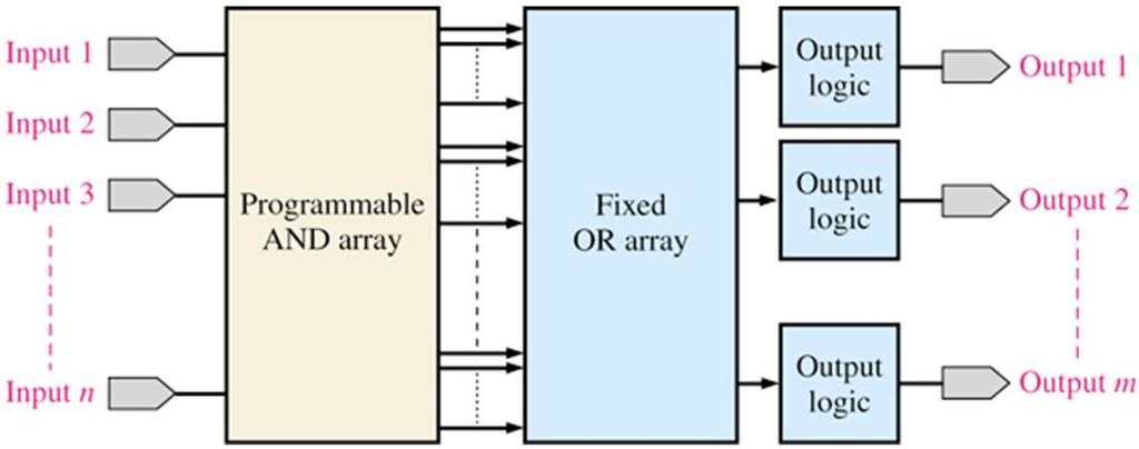
13 LSN 6 SPLD Classifications PROM (programmable read only memory) Set of no-programmable (fixed) AND gates that act as a decoder and a programmable OR array PLA (programmable logic array) Contains both a programmable OR and AND array PAL (programmable array logic) Contains a programmable AND array with a fixed OR array with output logic GAL (generic array logic) Reprogrammable AND array with a fixed OR array and programmable output logic

14 LSN 6 Programmable Array Logic

15 LSN 6 Programmable Array Logic Example: Show a programmed PAL representation for the SOP expression X = ABC + ABC + AB

16 LSN 6 Programmable Array Logic PAL output combinational logic Several common output logic configurations can be used together in a single PAL device Combinational output The output is used for an SOP function Typically available as active-high, active-low, or as a highimpedance disconnect state

17 LSN 6 Programmable Array Logic Combinational input/output The output function must feedback to be an input to the array or to be used to make the I/O pin an input only
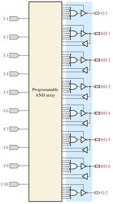
18 LSN 6 Programmable Array Logic


19 LSN 6 Generic Array Logic GAL Type of PAL with a reprogrammable array of AND gates SOP form
20 LSN 6 CPLD Contains multiple groups of PAL/GAL-like arrays with programmable interconnections Each PAL/GAL-like group is called a logic-arrayblock (LAB), function-block, or similar term Each group contains several PAL/GAL-like arrays called macrocells

21 LSN 6 CPLD
22 LSN 6 FPGA Contains an array of logic blocks with programmable row and column interconnected channels surrounded by programmable I/O blocks Most FPGA architectures is based on a type of memory called a look-up-table (LUT) instead of AND/OR gate arrays Each logic block contains several logic elements (LE)

23 LSN 6 FPGA


24 LSN 6 FPGA Lookup table Also called Function Generators (FGs) Capacity is limited by the number of inputs, not by the complexity Delay through the LUT is constant A B C D Combinatorial Logic Z A B C D Z
25 LSN 6 FPGA Programmable interconnections FPGAs typically use SRAM or antifuse to produce interconnection links between logic blocks Antifuse Melts to produce connection (NO) One-time programmable

26 LSN 6 FPGA SRAM On-chip SRAM cell controls the state of transistor connections between interconnect lines Reprogrammable by changing the program stored in the SRAM device
27 LSN 6 PLD Design Flow Start with an idea or specification that needs to be implemented Next begin the circuit design Schematics Hardware description languages Other methods (equations, etc.) Implementation of design Schematic capture Coding HDL Developing state diagrams
28 LSN 6 PLD Design Flow Synthesis of logic design Develop a model of design for target PLD Verification of logic design through simulation Simulation with test vectors and schematic simulators Formal verification using HDL simulators Various types of verification Logical correctness Static timing analysis In system verification
29 LSN 6 PLD Design Flow Program the internal circuitry of the PLD to implement the logic operations Download design to target device The programmed device has the same operation as its associated fixed-function logic circuit Programmed devices must be tested to ensure they operate as specified Verify on an expensive tester / in system (production) Verify in the lab with debug equipment (prototype)
30 LSN 6 PLD Programming Schematic entry User draws the logic design using graphical representations of standard logic components and their interconnections Text-based entry User enters a logic design using a Hardware Description Language (HDL) Verilog VHDL State-flow entry
31 LSN 6 Homework Reading Chapter 11.1 and 11.5 Assignment HW8 Chapter 11, problems 1, 4, 5, 16, and 17 References Documentation User Guides Xilinx white paper The Advantages of Migrating from Discrete 7400 Logic Devices to CPLDs FPGA & Structured ASIC Journal article All is Not SRAM
LSN 1 Digital Design Flow for PLDs
 LSN 1 Digital Design Flow for PLDs ECT357 Microprocessors I Department of Engineering Technology LSN 1 Programmable Logic Devices Functionless devices in base form Require programming to operate The logic
Programmable Logic Devices
 Programmable Logic Devices INTRODUCTION A programmable logic device or PLD is an electronic component used to build reconfigurable digital circuits. Unlike a logic gate, which has a fixed function, a PLD
PLAs & PALs. Programmable Logic Devices (PLDs) PLAs and PALs
 PLAs and PALs") PLAs & PALs Programmable Logic Devices (PLDs) PLAs and PALs PLAs&PALs By the late 1970s, standard logic devices were all the rage, and printed circuit boards were loaded with them. To offer the ultimate
PLAs & PALs Programmable Logic Devices (PLDs) PLAs and PALs PLAs&PALs By the late 1970s, standard logic devices were all the rage, and printed circuit boards were loaded with them. To offer the ultimate
Embedded Controller Design. CompE 270 Digital Systems - 5. Objective. Application Specific Chips. User Programmable Logic. Copyright 1998 Ken Arnold 1
 CompE 270 Digital Systems - 5 Programmable Logic Ken Arnold Objective Application Specific ICs Introduce User Programmable Logic Common Architectures Programmable Array Logic Address Decoding Example Development
Programmable Logic Devices UNIT II DIGITAL SYSTEM DESIGN
 Programmable Logic Devices UNIT II DIGITAL SYSTEM DESIGN 2 3 4 5 6 7 8 9 2 3 4 5 6 7 8 9 2 Implementation in Sequential Logic 2 PAL Logic Implementation Design Example: BCD to Gray Code Converter A B
DIGITAL SYSTEM FUNDAMENTALS (ECE421) DIGITAL ELECTRONICS FUNDAMENTAL (ECE4220. PROGRAMMABLE LOGIC DEVICES (PLDs)
 DIGITAL ELECTRONICS FUNDAMENTAL (ECE4220. PROGRAMMABLE LOGIC DEVICES (PLDs)") COURSE / CODE DIGITAL SYSTEM FUNDAMENTALS (ECE421) DIGITAL ELECTRONICS FUNDAMENTAL (ECE4220 PROGRAMMABLE LOGIC DEVICES (PLDs) A PLD, or programmable logic device, is an electronic component that is used
COURSE / CODE DIGITAL SYSTEM FUNDAMENTALS (ECE421) DIGITAL ELECTRONICS FUNDAMENTAL (ECE4220 PROGRAMMABLE LOGIC DEVICES (PLDs) A PLD, or programmable logic device, is an electronic component that is used
Evolution of Implementation Technologies. ECE 4211/5211 Rapid Prototyping with FPGAs. Gate Array Technology (IBM s) Programmable Logic
 Programmable Logic") ECE 42/52 Rapid Prototyping with FPGAs Dr. Charlie Wang Department of Electrical and Computer Engineering University of Colorado at Colorado Springs Evolution of Implementation Technologies Discrete devices:
ECE 42/52 Rapid Prototyping with FPGAs Dr. Charlie Wang Department of Electrical and Computer Engineering University of Colorado at Colorado Springs Evolution of Implementation Technologies Discrete devices:
ECE 331 Digital System Design
 ECE 331 Digital System Design Tristate Buffers, Read-Only Memories and Programmable Logic Devices (Lecture #17) The slides included herein were taken from the materials accompanying Fundamentals of Logic
Chapter 13 Programmable Logic Device Architectures
 Chapter 13 Programmable Logic Device Architectures Chapter 13 Objectives Selected areas covered in this chapter: Describing different categories of digital system devices. Describing different types of
FPGA. Logic Block. Plessey FPGA: basic building block here is 2-input NAND gate which is connected to each other to implement desired function.
 FPGA Logic block of an FPGA can be configured in such a way that it can provide functionality as simple as that of transistor or as complex as that of a microprocessor. It can used to implement different
CHAPTER 9 MULTIPLEXERS, DECODERS, AND PROGRAMMABLE LOGIC DEVICES
 CHAPTER 9 MULTIPLEXERS, DECODERS, AND PROGRAMMABLE LOGIC DEVICES This chapter in the book includes: Objectives Study Guide 9.1 Introduction 9.2 Multiplexers 9.3 Three-State Buffers 9.4 Decoders and Encoders
Introduction to Programmable Logic Devices (Class 7.2 2/28/2013)
") Introduction to Programmable Logic Devices (Class 7.2 2/28/2013) CSE 2441 Introduction to Digital Logic Spring 2013 Instructor Bill Carroll, Professor of CSE Today s Topics Complexity issues Implementation
Introduction to Programmable Logic Devices (Class 7.2 2/28/2013) CSE 2441 Introduction to Digital Logic Spring 2013 Instructor Bill Carroll, Professor of CSE Today s Topics Complexity issues Implementation
Computer Structure. Unit 2: Memory and programmable devices
 Computer Structure Unit 2: Memory and programmable devices Translated from Francisco Pérez García (fperez at us.es) by Mª Carmen Romero (mcromerot at us.es, Office G1.51, 954554324) Electronic Technology
CMPE 415 Programmable Logic Devices FPGA Technology I
 Department of Computer Science and Electrical Engineering CMPE 415 Programmable Logic Devices FPGA Technology I Prof. Ryan Robucci Some slides (blue-frame) developed by Jim Plusquellic Some images credited
FPGA for Complex System Implementation. National Chiao Tung University Chun-Jen Tsai 04/14/2011
 FPGA for Complex System Implementation National Chiao Tung University Chun-Jen Tsai 04/14/2011 About FPGA FPGA was invented by Ross Freeman in 1989 SRAM-based FPGA properties Standard parts Allowing multi-level
Memory and Programmable Logic
 Memory and Programmable Logic Memory units allow us to store and/or retrieve information Essentially look-up tables Good for storing data, not for function implementation Programmable logic device (PLD),
Digital Electronics 27. Digital System Design using PLDs
 1 Module -27 Digital System Design 1. Introduction 2. Digital System Design 2.1 Standard (Fixed function) ICs based approach 2.2 Programmable ICs based approach 3. Comparison of Digital System Design approaches
FYSE420 DIGITAL ELECTRONICS. Lecture 7
 FYSE420 DIGITAL ELECTRONICS Lecture 7 1 [1] [2] [3] DIGITAL LOGIC CIRCUIT ANALYSIS & DESIGN Nelson, Nagle, Irvin, Carrol ISBN 0-13-463894-8 DIGITAL DESIGN Morris Mano Fourth edition ISBN 0-13-198924-3
An Introduction to Programmable Logic
 Outline An Introduction to Programmable Logic 3 November 24 Transistors Logic Gates CPLD Architectures FPGA Architectures Device Considerations Soft Core Processors Design Example Quiz Semiconductors Semiconductor
Lecture 13: Memory and Programmable Logic
 Lecture 13: Memory and Programmable Logic Syed M. Mahmud, Ph.D ECE Department Wayne State University Aby K George, ECE Department, Wayne State University Contents Introduction Random Access Memory Memory
PROGRAMMABLE MODULES SPECIFICATION OF PROGRAMMABLE COMBINATIONAL AND SEQUENTIAL MODULES
 PROGRAMMABLE MODULES SPECIFICATION OF PROGRAMMABLE COMBINATIONAL AND SEQUENTIAL MODULES. psa. rom. fpga THE WAY THE MODULES ARE PROGRAMMED NETWORKS OF PROGRAMMABLE MODULES EXAMPLES OF USES Programmable
Memory and Programmable Logic
 Digital Circuit Design and Language Memory and Programmable Logic Chang, Ik Joon Kyunghee University Memory Classification based on functionality ROM : Read-Only Memory RWM : Read-Write Memory RWM NVRWM
FPGA Programming Technology
 FPGA Programming Technology Static RAM: This Xilinx SRAM configuration cell is constructed from two cross-coupled inverters and uses a standard CMOS process. The configuration cell drives the gates of
Chapter 5: ASICs Vs. PLDs
 Chapter 5: ASICs Vs. PLDs 5.1 Introduction A general definition of the term Application Specific Integrated Circuit (ASIC) is virtually every type of chip that is designed to perform a dedicated task.
Programmable Logic Devices Introduction CMPE 415. Programmable Logic Devices
 Instructor: Professor Jim Plusquellic Programmable Logic Devices Text: The Design Warrior s Guide to FPGAs, Devices, Tools and Flows, Clive "Max" Maxfield, ISBN: 0-7506-7604-3 Modeling, Synthesis and Rapid
Digital Design Methodology
 Digital Design Methodology Prof. Soo-Ik Chae Digital System Designs and Practices Using Verilog HDL and FPGAs @ 2008, John Wiley 1-1 Digital Design Methodology (Added) Design Methodology Design Specification
Digital Design Methodology (Revisited) Design Methodology: Big Picture
 Design Methodology: Big Picture") Digital Design Methodology (Revisited) Design Methodology Design Specification Verification Synthesis Technology Options Full Custom VLSI Standard Cell ASIC FPGA CS 150 Fall 2005 - Lec #25 Design Methodology
Digital Design Methodology (Revisited) Design Methodology Design Specification Verification Synthesis Technology Options Full Custom VLSI Standard Cell ASIC FPGA CS 150 Fall 2005 - Lec #25 Design Methodology
ELCT 912: Advanced Embedded Systems
 Advanced Embedded Systems Lecture 2: Memory and Programmable Logic Dr. Mohamed Abd El Ghany, Memory Random Access Memory (RAM) Can be read and written Static Random Access Memory (SRAM) Data stored so
Design Methodologies and Tools. Full-Custom Design
 Design Methodologies and Tools Design styles Full-custom design Standard-cell design Programmable logic Gate arrays and field-programmable gate arrays (FPGAs) Sea of gates System-on-a-chip (embedded cores)
Presentation 4: Programmable Combinational Devices
 Presentation 4: Programmable Combinational Devices Asst. Prof Dr. Ahmet ÖZKURT DEUEEE Based on the Presentation by Prof. Kim, Young Ho Dept. of Information Computer Engineering E-mail : yhkim@hyowon.cs.pusan.ac.kr
Hardware Design with VHDL PLDs I ECE 443. FPGAs can be configured at least once, many are reprogrammable.
 PLDs, ASICs and FPGAs FPGA definition: Digital integrated circuit that contains configurable blocks of logic and configurable interconnects between these blocks. Key points: Manufacturer does NOT determine
FPGA Based Digital Design Using Verilog HDL
 FPGA Based Digital Design Using Course Designed by: IRFAN FAISAL MIR ( Verilog / FPGA Designer ) irfanfaisalmir@yahoo.com * Organized by Electronics Division Integrated Circuits Uses for digital IC technology
Programmable Logic Devices
 Programmable Logic Devices Luis Entrena, Celia López, Mario García, Enrique San Millán Universidad Carlos III de Madrid Outline Tecnologies for implementing programmable circuits Simple Programmable Logic
Lecture (1) Introduction to FPGA. 1. The History of Programmable Logic
 Introduction to FPGA. 1. The History of Programmable Logic") Lecture (1) Introduction to FPGA 1. The History of Programmable Logic By the late 1970s, standard logic devices were all the rage, and printed circuit boards were loaded with them. Then someone asked,
Lecture (1) Introduction to FPGA 1. The History of Programmable Logic By the late 1970s, standard logic devices were all the rage, and printed circuit boards were loaded with them. Then someone asked,
Basic FPGA Architectures. Actel FPGAs. PLD Technologies: Antifuse. 3 Digital Systems Implementation Programmable Logic Devices
 3 Digital Systems Implementation Programmable Logic Devices Basic FPGA Architectures Why Programmable Logic Devices (PLDs)? Low cost, low risk way of implementing digital circuits as application specific
Programmable Logic Devices (PLDs) >Programmable Array Logic (PALs) >Programmable Logic Arrays (PLAs) PAL/GAL 16V8 CPLD: Altera s MAX 3064 & MAX V
 >Programmable Array Logic (PALs) >Programmable Logic Arrays (PLAs) PAL/GAL 16V8 CPLD: Altera s MAX 3064 & MAX V") Menu Look into my... Programmable Logic Devices (PLDs) >Programmable Array Logic (PALs) >Programmable Logic Arrays (PLAs) PAL/GAL 16V8 CPLD: Altera s MAX 3064 & MAX V Read Roth: Sections 9.6-9.8 (Sections
Menu Look into my... Programmable Logic Devices (PLDs) >Programmable Array Logic (PALs) >Programmable Logic Arrays (PLAs) PAL/GAL 16V8 CPLD: Altera s MAX 3064 & MAX V Read Roth: Sections 9.6-9.8 (Sections
Digital Integrated Circuits
 Digital Integrated Circuits Lecture 9 Jaeyong Chung Robust Systems Laboratory Incheon National University DIGITAL DESIGN FLOW Chung EPC6055 2 FPGA vs. ASIC FPGA (A programmable Logic Device) Faster time-to-market
Design Methodologies. Full-Custom Design
 Design Methodologies Design styles Full-custom design Standard-cell design Programmable logic Gate arrays and field-programmable gate arrays (FPGAs) Sea of gates System-on-a-chip (embedded cores) Design
Very Large Scale Integration (VLSI)
") Very Large Scale Integration (VLSI) Lecture 6 Dr. Ahmed H. Madian Ah_madian@hotmail.com Dr. Ahmed H. Madian-VLSI 1 Contents FPGA Technology Programmable logic Cell (PLC) Mux-based cells Look up table PLA
Very Large Scale Integration (VLSI) Lecture 6 Dr. Ahmed H. Madian Ah_madian@hotmail.com Dr. Ahmed H. Madian-VLSI 1 Contents FPGA Technology Programmable logic Cell (PLC) Mux-based cells Look up table PLA
INTRODUCTION TO FPGA ARCHITECTURE
 3/3/25 INTRODUCTION TO FPGA ARCHITECTURE DIGITAL LOGIC DESIGN (BASIC TECHNIQUES) a b a y 2input Black Box y b Functional Schematic a b y a b y a b y 2 Truth Table (AND) Truth Table (OR) Truth Table (XOR)
Copyright by Syed Ashad Mustufa Younus Copyright by Syed Ashad Mustufa Younus
 Copyright by Syed Ashad Mustufa Younus Copyright by Syed Ashad Mustufa Younus Microcontroller & Applications Week 2 Instructor: Syed Ashad Mustufa Younus HP: +92 (0) 300 240 8943 Email: :sashad@iqra.edu.pks
UNIT V (PROGRAMMABLE LOGIC DEVICES)
") UNIT V (PROGRAMMABLE LOGIC DEVICES) Introduction There are two types of memories that are used in digital systems: Random-access memory(ram): perform both the write and read operations. Read-only memory(rom):
UNIT V (PROGRAMMABLE LOGIC DEVICES) Introduction There are two types of memories that are used in digital systems: Random-access memory(ram): perform both the write and read operations. Read-only memory(rom):
Section 6. Memory Components Chapter 5.7, 5.8 Physical Implementations Chapter 7 Programmable Processors Chapter 8
 Section 6 Memory Components Chapter 5.7, 5.8 Physical Implementations Chapter 7 Programmable Processors Chapter 8 Types of memory Two major types of memory Volatile When power to the device is removed
ELCT 501: Digital System Design
 ELCT 501: Digital System Lecture 3: Memory and Programmable Logic (continue) Dr. Mohamed Abd El Ghany, Memory Model 32-bit address space can address up to 4 GB (2 32 ) different memory locations 0x00000000
CPLDs vs. FPGAs: Comparing High-Capacity Programmable Logic
 PIB 18 CPLDs vs. FPGAs: Comparing High-Capacity Programmable Logic CPLDs vs. FPGAs Comparing High-Capacity Programmable Logic February 1995, ver. 1 Product Information Bulletin 18 Introduction The high-capacity
Read-only memory Implementing logic with ROM Programmable logic devices Implementing logic with PLDs Static hazards
 Points Addressed in this Lecture Lecture 7: ROM Programmable Logic Devices Professor Peter Cheung Department of EEE, Imperial College London Read-only memory Implementing logic with ROM Programmable logic
Programmable Logic Devices (PLDs)
") Programmable Logic Devices (PLDs) 212: Digital Design I, week 13 PLDs basically store binary information in a volatile/nonvolatile device. Data is specified by designer and physically inserted (Programmed)
Programmable Logic Devices (PLDs) 212: Digital Design I, week 13 PLDs basically store binary information in a volatile/nonvolatile device. Data is specified by designer and physically inserted (Programmed)
Follow-up question: now, comment on what each of these acronyms actually means, going beyond a mere recitation of the definition.
 Question 1 Define the following acronyms as they apply to digital logic circuits: ASIC PAL PLA PLD CPLD FPGA file 03041 Answer 1 ASIC: Application-Specific Integrated Circuit PAL: Programmable Array Logic
8051 INTERFACING TO EXTERNAL MEMORY
 8051 INTERFACING TO EXTERNAL MEMORY Memory Capacity The number of bits that a semiconductor memory chip can store Called chip capacity It can be in units of Kbits (kilobits), Mbits (megabits), and so on
Programmable logic technology
 Programmable logic technology This worksheet and all related files are licensed under the Creative Commons Attribution License, version 1.0. To view a copy of this license, visit http://creativecommons.org/licenses/by/1.0/,
Unit 6 1.Random Access Memory (RAM) Chapter 3 Combinational Logic Design 2.Programmable Logic
 Chapter 3 Combinational Logic Design 2.Programmable Logic") EE 200: Digital Logic Circuit Design Dr Radwan E Abdel-Aal, COE Unit 6.Random Access Memory (RAM) Chapter 3 Combinational Logic Design 2. Logic Logic and Computer Design Fundamentals Part Implementation
EE 200: Digital Logic Circuit Design Dr Radwan E Abdel-Aal, COE Unit 6.Random Access Memory (RAM) Chapter 3 Combinational Logic Design 2. Logic Logic and Computer Design Fundamentals Part Implementation
Programmable Logic. Any other approaches?
 Programmable Logic So far, have only talked about PALs (see 22V10 figure next page). What is the next step in the evolution of PLDs? More gates! How do we get more gates? We could put several PALs on one
Outline. Field Programmable Gate Arrays. Programming Technologies Architectures. Programming Interfaces. Historical perspective
 Outline Field Programmable Gate Arrays Historical perspective Programming Technologies Architectures PALs, PLDs,, and CPLDs FPGAs Programmable logic Interconnect network I/O buffers Specialized cores Programming
Programmable Logic Devices FPGA Architectures II CMPE 415. Overview This set of notes introduces many of the features available in the FPGAs of today.
 Overview This set of notes introduces many of the features available in the FPGAs of today. The majority use SRAM based configuration cells, which allows fast reconfiguation. Allows new design ideas to
Introduction to Digital Logic Missouri S&T University CPE 2210 Hardware Implementations
 Introduction to Digital Logic Missouri S&T University CPE 2210 Hardware Implementations Egemen K. Çetinkaya Egemen K. Çetinkaya Department of Electrical & Computer Engineering Missouri University of Science
Review: Chip Design Styles
 MPT-50 Introduction to omputer Design SFU, Harbour entre, Spring 007 Lecture 9: Feb. 6, 007 Programmable Logic Devices (PLDs) - Read Only Memory (ROM) - Programmable Array Logic (PAL) - Programmable Logic
Hardware Synthesis. References
 Hardware Synthesis MidiaReshadi CE Department Science and research branch of Islamic Azad University Email: ce.srbiau@gmail.com 1 References 2 1 Chapter 1 Digital Design Using VHDL and PLDs 3 Some Definitions
Design Methodologies
 Design Methodologies 1981 1983 1985 1987 1989 1991 1993 1995 1997 1999 2001 2003 2005 2007 2009 Complexity Productivity (K) Trans./Staff - Mo. Productivity Trends Logic Transistor per Chip (M) 10,000 0.1
Memory and Programmable Logic
 Memory and Programmable Logic Mano & Ciletti Chapter 7 By Suleyman TOSUN Ankara University Outline RAM Memory decoding Error detection and correction ROM Programmable Logic Array (PLA) Programmable Array
Field Program mable Gate Arrays
 Field Program mable Gate Arrays M andakini Patil E H E P g r o u p D H E P T I F R SERC school NISER, Bhubaneshwar Nov 7-27 2017 Outline Digital electronics Short history of programmable logic devices
FPGA Implementations
 FPGA Implementations Smith Text: Chapters 4-8 Online version at: http://www10.edacafe.com/book/asic/asics.php Topic outline Chapter 4 Programmable ASIC technologies Chapter 5 Programmable logic cells Chapter
Actel s SX Family of FPGAs: A New Architecture for High-Performance Designs
 Actel s SX Family of FPGAs: A New Architecture for High-Performance Designs A Technology Backgrounder Actel Corporation 955 East Arques Avenue Sunnyvale, California 94086 April 20, 1998 Page 2 Actel Corporation
Introduction PLD - Programmable Logic Device Hardware focus typically on Microprocessor, microcontroller, and microcomputer
 Programmable Logic Devices Overview In this lesson we will Begin with an overview of programmable logic devices - PLDs. Motivate the use of PLDs. Introduce some of the basic underlying concepts in PLDs.
DIGITAL DESIGN TECHNOLOGY & TECHNIQUES
 DIGITAL DESIGN TECHNOLOGY & TECHNIQUES CAD for ASIC Design 1 INTEGRATED CIRCUITS (IC) An integrated circuit (IC) consists complex electronic circuitries and their interconnections. William Shockley et
EECS150 - Digital Design Lecture 6 - Field Programmable Gate Arrays (FPGAs)
") EECS150 - Digital Design Lecture 6 - Field Programmable Gate Arrays (FPGAs) September 12, 2002 John Wawrzynek Fall 2002 EECS150 - Lec06-FPGA Page 1 Outline What are FPGAs? Why use FPGAs (a short history
EECS150 - Digital Design Lecture 6 - Field Programmable Gate Arrays (FPGAs) September 12, 2002 John Wawrzynek Fall 2002 EECS150 - Lec06-FPGA Page 1 Outline What are FPGAs? Why use FPGAs (a short history
(ii) Simplify and implement the following SOP function using NOR gates:
 Simplify and implement the following SOP function using NOR gates:") DHANALAKSHMI COLLEGE OF ENGINEERING DEPARTMENT OF ELECTRONICS AND COMMUNICATION ENGINEERING EE6301 DIGITAL LOGIC CIRCUITS UNIT I NUMBER SYSTEMS AND DIGITAL LOGIC FAMILIES PART A 1. How can an OR gate be
DHANALAKSHMI COLLEGE OF ENGINEERING DEPARTMENT OF ELECTRONICS AND COMMUNICATION ENGINEERING EE6301 DIGITAL LOGIC CIRCUITS UNIT I NUMBER SYSTEMS AND DIGITAL LOGIC FAMILIES PART A 1. How can an OR gate be
Outline. EECS150 - Digital Design Lecture 6 - Field Programmable Gate Arrays (FPGAs) FPGA Overview. Why FPGAs?
 FPGA Overview. Why FPGAs?") EECS150 - Digital Design Lecture 6 - Field Programmable Gate Arrays (FPGAs) September 12, 2002 John Wawrzynek Outline What are FPGAs? Why use FPGAs (a short history lesson). FPGA variations Internal logic
EECS150 - Digital Design Lecture 6 - Field Programmable Gate Arrays (FPGAs) September 12, 2002 John Wawrzynek Outline What are FPGAs? Why use FPGAs (a short history lesson). FPGA variations Internal logic
Configurable Embedded Systems: Using Programmable Logic to Compress Embedded System Design Cycles
 Class 330 Configurable Embedded Systems: Using Programmable Logic to Compress Embedded System Design Cycles Steven Knapp (sknapp) Arye Ziklik (arye) Triscend Corporation www.triscend.com Copyright 1998,
Usable gates 600 1,250 2,500 5,000 10,000 Macrocells Logic array blocks Maximum user I/O
 MAX 3000A Programmable Logic Device Family June 2006, ver. 3.5 Data Sheet Features... High performance, low cost CMOS EEPROM based programmable logic devices (PLDs) built on a MAX architecture (see Table
CS310 Embedded Computer Systems. Maeng
 1 INTRODUCTION (PART II) Maeng Three key embedded system technologies 2 Technology A manner of accomplishing a task, especially using technical processes, methods, or knowledge Three key technologies for
Field Programmable Gate Array (FPGA)
") Field Programmable Gate Array (FPGA) Lecturer: Krébesz, Tamas 1 FPGA in general Reprogrammable Si chip Invented in 1985 by Ross Freeman (Xilinx inc.) Combines the advantages of ASIC and uc-based systems
Field Programmable Gate Array (FPGA) Lecturer: Krébesz, Tamas 1 FPGA in general Reprogrammable Si chip Invented in 1985 by Ross Freeman (Xilinx inc.) Combines the advantages of ASIC and uc-based systems
Microcontroller Systems. ELET 3232 Topic 11: General Memory Interfacing
 Microcontroller Systems ELET 3232 Topic 11: General Memory Interfacing 1 Objectives To become familiar with the concepts of memory expansion and the data and address bus To design embedded systems circuits
Programmable Logic Devices
 Programmable Logic Devices Programmable Logic Devices Fig. (1) General structure of PLDs Programmable Logic Device (PLD): is an integrated circuit with internal logic gates and/or connections that can
MEMORY AND PROGRAMMABLE LOGIC
 MEMORY AND PROGRAMMABLE LOGIC Memory is a device where we can store and retrieve information It can execute a read and a write Programmable Logic is a device where we can store and retrieve information
Sistemas Digitais I LESI - 2º ano
 Sistemas Digitais I LESI - 2º ano Lesson 9 - Memory, CPLDs and FPGAs Prof. João Miguel Fernandes (miguel@di.uminho.pt) Dept. Informática UNIVERSIDADE DO MINHO ESCOLA DE ENGENHARIA - Memory - Any sequential
FPGA: What? Why? Marco D. Santambrogio
 FPGA: What? Why? Marco D. Santambrogio marco.santambrogio@polimi.it 2 Reconfigurable Hardware Reconfigurable computing is intended to fill the gap between hardware and software, achieving potentially much
Digital Systems Design with PLDs and FPGAs Kuruvilla Varghese Department of Electronic Systems Engineering Indian Institute of Science Bangalore
 Digital Systems Design with PLDs and FPGAs Kuruvilla Varghese Department of Electronic Systems Engineering Indian Institute of Science Bangalore Lecture-31 Evolution of PLDs So welcome to this lecture
PALs, GALs & CUPL. What is Programmable Logic?
 PALs, GALs & CUPL A lesson on Programmable Logic Devices and programming them using CUPL What is Programmable Logic? Digital integrated circuits where the Boolean function can be determined by the user.
Chapter 6 Selected Design Topics
 Logic and Computer Design Fundamentals Chapter 6 Selected Design Topics Part 4 Programmable Implementation Technologies Charles Kime & Thomas Kaminski 2008 Pearson Education, Inc. (Hyperlinks are active
UNIT - V MEMORY P.VIDYA SAGAR ( ASSOCIATE PROFESSOR) Department of Electronics and Communication Engineering, VBIT
 Department of Electronics and Communication Engineering, VBIT") UNIT - V MEMORY P.VIDYA SAGAR ( ASSOCIATE PROFESSOR) contents Memory: Introduction, Random-Access memory, Memory decoding, ROM, Programmable Logic Array, Programmable Array Logic, Sequential programmable
UNIT - V MEMORY P.VIDYA SAGAR ( ASSOCIATE PROFESSOR) contents Memory: Introduction, Random-Access memory, Memory decoding, ROM, Programmable Logic Array, Programmable Array Logic, Sequential programmable
Field Programmable Gate Array
 Field Programmable Gate Array System Arch 27 (Fire Tom Wada) What is FPGA? System Arch 27 (Fire Tom Wada) 2 FPGA Programmable (= reconfigurable) Digital System Component Basic components Combinational
Copyright 2011 R.S.R. Electronics, Inc. All rights reserved. 04/11. Ver. 1.0web
 For XILINX WebPack Copyright 2011 R.S.R. Electronics, Inc. All rights reserved. 04/11 Ver. 1.0web 1 Table of Contents 1.0 INTRODUCTION...3 2.0 GENERAL DESCRIPTION...5 3.0 BRIEF DESCRIPTION Of PLDT-3 BOARD...6
New Logic Module for secured FPGA based system
 International Journal of Electronics and Communication Engineering. ISSN 0974-2166 Volume 5, Number 4 (2012), pp. 533-543 International Research Publication House http://www.irphouse.com New Logic Module
CMPE 415 Programmable Logic Devices Introduction
 Department of Computer Science and Electrical Engineering CMPE 415 Programmable Logic Devices Introduction Prof. Ryan Robucci What are FPGAs? Field programmable Gate Array Typically re programmable as
DIGITAL CIRCUIT LOGIC UNIT 9: MULTIPLEXERS, DECODERS, AND PROGRAMMABLE LOGIC DEVICES
 DIGITAL CIRCUIT LOGIC UNIT 9: MULTIPLEXERS, DECODERS, AND PROGRAMMABLE LOGIC DEVICES 1 Learning Objectives 1. Explain the function of a multiplexer. Implement a multiplexer using gates. 2. Explain the
Programmable Logic Design Techniques I
 PHY 440 Lab14: Programmable Logic Design Techniques I The design of digital circuits is a multi-step process. It starts with specifications describing what the circuit must do. Defining what a circuit
10 2 ADDRESS DECODING:
 10 2 ADDRESS DECODING: Simple NAND Gate Decoder: When the 2K 8 EPROM is used, address connections A10 A0 of the 8088 are connected to address inputs A10 A0 of the EPROM. The remaining nine address pins
Design of Embedded Processors
 Design of Embedded Processors Lesson 20 Field Programmable Gate Arrays and Applications Instructional Objectives After going through this lesson the student will be able to Define what is a field programmable
Chapter 10: Design Options of Digital Systems
 Chapter 10: Design Options of Digital Systems Prof. Ming-Bo Lin Department of Electronic Engineering National Taiwan University of Science and Technology Digital System Designs and Practices Using Verilog
ECE 636. Reconfigurable Computing. Lecture 2. Field Programmable Gate Arrays I
 ECE 636 Reconfigurable Computing Lecture 2 Field Programmable Gate Arrays I Overview Anti-fuse and EEPROM-based devices Contemporary SRAM devices - Wiring - Embedded New trends - Single-driver wiring -
Programmable Logic Devices I. EECE143 Lecture 4. PALs, GALs & CUPL. A lesson on Programmable Logic Devices and programming them using CUPL
 PALs, GALs & CUPL A lesson on Programmable Logic Devices and programming them using CUPL What is Programmable Logic? Digital integrated circuits where the Boolean function can be determined by the user.
Today. Comments about assignment Max 1/T (skew = 0) Max clock skew? Comments about assignment 3 ASICs and Programmable logic Others courses
 Max clock skew? Comments about assignment 3 ASICs and Programmable logic Others courses") Today Comments about assignment 3-43 Comments about assignment 3 ASICs and Programmable logic Others courses octor Per should show up in the end of the lecture Mealy machines can not be coded in a single
Today Comments about assignment 3-43 Comments about assignment 3 ASICs and Programmable logic Others courses octor Per should show up in the end of the lecture Mealy machines can not be coded in a single
Boolean Algebra. BME208 Logic Circuits Yalçın İŞLER
 Boolean Algebra BME28 Logic Circuits Yalçın İŞLER islerya@yahoo.com http://me.islerya.com 5 Boolean Algebra /2 A set of elements B There exist at least two elements x, y B s. t. x y Binary operators: +
Evolution of CAD Tools & Verilog HDL Definition
 Evolution of CAD Tools & Verilog HDL Definition K.Sivasankaran Assistant Professor (Senior) VLSI Division School of Electronics Engineering VIT University Outline Evolution of CAD Different CAD Tools for
ProASIC PLUS FPGA Family
 ProASIC PLUS FPGA Family Key Features Reprogrammable /Nonvolatile Flash Technology Low Power Secure Single Chip/Live at Power Up 1M Equivalent System Gates Cost Effective ASIC Alternative ASIC Design Flow
PROGRAMMABLE LOGIC DEVICES
 PROGRAMMABLE LOGIC DEVICES Programmable logic devices (PLDs) are used for designing logic circuits. PLDs can be configured by the user to perform specific functions. The different types of PLDs available
FPGA for Dummies. Introduc)on to Programmable Logic
on to Programmable Logic") FPGA for Dummies Introduc)on to Programmable Logic FPGA for Dummies Historical introduc)on, where we come from; FPGA Architecture: Ø basic blocks (Logic, FFs, wires and IOs); Ø addi)onal elements; FPGA
FPGA for Dummies Introduc)on to Programmable Logic FPGA for Dummies Historical introduc)on, where we come from; FPGA Architecture: Ø basic blocks (Logic, FFs, wires and IOs); Ø addi)onal elements; FPGA
Topics. FPGA Design EECE 277. Interconnect and Logic Elements Part 2. Laboratory Assignment #1 Save Everything!!! Guest Lecture
 FPGA Design EECE 277 Interconnect and Logic Elements Part 2 Dr. William H. Robinson February 4, 2005 http://eecs.vanderbilt.edu/courses/eece277/ Topics The sky is falling. I must go and tell the King.
EE 466/586 VLSI Design. Partha Pande School of EECS Washington State University
 EE 466/586 VLSI Design Partha Pande School of EECS Washington State University pande@eecs.wsu.edu Lecture 18 Implementation Methods The Design Productivity Challenge Logic Transistors per Chip (K) 10,000,000.10m
CHAPTER 12 ARRAY SUBSYSTEMS [ ] MANJARI S. KULKARNI
![CHAPTER 12 ARRAY SUBSYSTEMS [ ] MANJARI S. KULKARNI](/thumbs/76/73997056.jpg "CHAPTER 12 ARRAY SUBSYSTEMS [ ] MANJARI S. KULKARNI") CHAPTER 2 ARRAY SUBSYSTEMS [2.4-2.9] MANJARI S. KULKARNI OVERVIEW Array classification Non volatile memory Design and Layout Read-Only Memory (ROM) Pseudo nmos and NAND ROMs Programmable ROMS PROMS, EPROMs,
CHAPTER 2 ARRAY SUBSYSTEMS [2.4-2.9] MANJARI S. KULKARNI OVERVIEW Array classification Non volatile memory Design and Layout Read-Only Memory (ROM) Pseudo nmos and NAND ROMs Programmable ROMS PROMS, EPROMs,