SheevaPlug Development Kit Reference Design. Rev 1.2
|
|
|
- Buck Cooper
- 6 years ago
- Views:
Transcription
1 SheevaPlug Development Kit Reference Design Rev 1.2
2 INTRODUCTION...4 SECTION 1 OVERVIEW SHEEVAPLUG DESCRIPTION....6 Figure 1.1: SHEEVAPLUG Components and JTAG test card...6 Figure 1.2: SheevaPlug controller and JTAG inside the box...7 Figure 1.3: Front Panel...8 Figure 1.4: side Panel...8 Figure 1.5: Bottom Panel...9 Figure 1.6: Side Panel...10 Figure 1.7: Block Diagram...10 SECTION 2 SETTING UP THE SHEEVAPLUG DEVKIT BOARD REQUIREMENTS LAYOUT JUMPER SETTINGS AC POWER CONSUMPTION DC POWER CONSUMPTION DIMENSIONS (L X W X D) POWER REQUIREMENT DRIVE CONNECTION NETWORK CONNECTION...12 SECTION 3 CIRCUITRY DESCRIPTION TOP LEVEL PROCESSOR IO EXPANSION EXTERNAL BUS INTERFACE NAND Flash memory DDR2 Memory USB Ethernet POWER AND CRYSTAL CLOCKS JTAG INTERFACE AND RESET SERIAL INTERFACE OPEN OCD INTERFACE LAYOUT DRAWING SHEEVAPLUG PCB STACK UP JTAG V2 PCB DRAWING AND PCB STACK UP...16 SECTION 4 ON-BOARD SOFTWARE FLASH MEMORY Flash Memory Organization FLASH WRITE ACCESS FUNCTIONAL TEST SOFTWARE...18 SECTION 5 APPENDIX A- SCHEMATICS THE FOLLOWING SCHEMATICS ARE APPENDED:...20 Figure 5.1 block diagram...20 Figure 5.2 DDR2 block...20 Figure 5.3 DDR2 Bank Figure 5.4 DDR2 Bank Figure 5.5 NAND FLASH interface...20 Figure 5.6 Ethernet Interface...20 Figure F6281 VCC supplies...20 Figure 5.8 SHEEVAPLUG DC-DC distributions...20 Figure F6281 JTAG and USB interface...20 Figure 5.10 GPIOS and Test connector interface...20 Figure 5.11 SHEEVAPLUG JTAG V2 SDIO interface...20 Rev1.2 SheevaPlug Development Kit purpose only 2
3 Figure 5.12 Figure 5.13 SHEEVAPLUG FDT2322D interface...20 SHEEVAPLUG BOM...21 Rev1.2 SheevaPlug Development Kit purpose only 3
4 Introduction The SheevaPlug DevKit Reference Design demonstrates the capabilities of the Marvell high-performance MV88F6281 general purpose integrated SOC controller with CPU. Network connectivity in the SheevaPlug Development Kit is provided through Gigabit Ethernet and peripheral connectivity is provided through USB2.0 The SheevaPlug Development Kit includes the following components: Marvell high-performance MV88F6281 general purpose controller with integrated CPU running at 1200 MHz Double Data Rate II (DDR2) SDRAM memory on board: Up to 4 one Gigabit x8 device -16 bit width, for a total of 512 MB running at a clock frequency of 400 MHz, data rate at 800 MHz Gigabit Ethernet port: On-board Gigabit Ethernet port on RJ-45 connector (J1) Connected to 88E1116R Marvell PHY using RGMII interface. USB 2.0 Interface: Host to Device USB adapter (J6) NAND Flash MB, U-boot, included Kernel, and File System RS-232 COM port connector by UART FDT2322D adapter via a mini USB connector. ARM-compliant JTAG connector, also via a mini USB connector Rev1.2 SheevaPlug Development Kit purpose only 4
5 Shipping Contents The SheevaPlug Development Kit package is shipped with the following components: One SheevaPlug including the SheevaPlug board and Debug adapter USB Cable Ethernet Cable CD containing software and documentation North American Power Cord (7A/125V) The power cord can be used instead of the A/C plug on the SheevaPlug. To remove the A/C plug, the suggested method is to hold the SheevaPlug with both hands, with the A/C plug facing you and away from you. Use both your thumbs to press the plastic just below the prongs and push down and away. Related Documentation. 88F6281, 88F6192, and 88F6180 Functional Specifications (Document Number MV-S ). 88F6192 Hardware Specifications (Document Number MV-S ). SheevaPlug Schematic and PCB layout. 88F6180, 88F6192, and 88F6281 Functional Errata, Interface Guidelines, and Restrictions (Document Number MV-S ) Technical Support Marvell may have updated the collateral that was shipped with this product. Contact your local sales representative or FAE for updates. This collateral information includes the following: Assembly, BOM, and schematic and monitor source code. Rev1.2 SheevaPlug Development Kit purpose only 5

6 Section 1 Overview 1.1 SheevaPlug description. The main board components are detailed in Figure 1. 1 Figure 1.1: SheevaPlug board Components and JTAG adapter card Master Reset 512MB DDR2 400MHZ Power connector 512 MB NAND Flash 88F6281 SDIO Slot 88E1116R Mini USB JTAG / UART USB 2.0 Gigabit RJ45 Rev1.2 SheevaPlug Development Kit purpose only 6


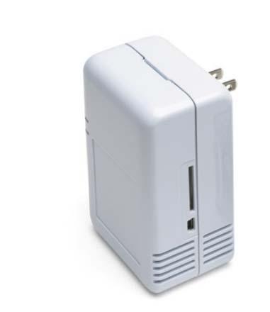
7 Figure 1.2: SheevaPlug and JTAG inside the box AC DC Module Rev1.2 SheevaPlug Development Kit purpose only 7


8 Figure 1.3: Front Panel Figure 1.4: side Panel Rev1.2 SheevaPlug Development Kit purpose only 8


9 Figure 1.5: Bottom Panel Rev1.2 SheevaPlug Development Kit purpose only 9
10 Figure 1.6: Side Panel Figure 1.7: Block Diagram HW Block Diagram DDR2 4x8-1Gigabit (512MB) Reset JTAG-ICE Sheeva CPU Processor 1. 2Ghz 64bits, 200Mhz DDR2 controller DMA Engines x4 FDT2322D Nand Flash 512MB Mbus bridge Security Engine MiniUSB SDIO Slot Gpps/ Uarts/ NFlash/SPI interface SPDIF/I2S/ Audio interface PCI- Express with Serdes x1 interface MBUS MHZ TS Video Interface TDM(SLIC CODEC) interface SATAII with PHYs x2 interface RJ45 88F1116R GigaSerdes Gigabit x2 interface Usb 2.0 with Phy interface USB Type A 88F6182 Reset Clock Generator Voltage Regulator RTC battery Rev1.2 SheevaPlug Development Kit purpose only 10
 - Ethernet connection")
11 Section 2 Setting up the SheevaPlug Development Kit Board 2.1 Requirements Requirements in order to set up the plug board are: - The SheevaPlug itself - AC power plug or AC cord - USB cable type A to min B (UART and Open OCD connection) - Ethernet connection 2.2 Layout Figure 2-1 shows the layout of the SheevaPlug board 2.3 Jumper Settings There is no jumper setting for this board. The processor clock is running at 1.2 GHz, DDR2 clock frequency is 400 MHz, and TCLK is 200MHz internally. 2.4 AC Power Consumption Rev1.2 SheevaPlug Development Kit purpose only 11

12 TBA 2.5 DC Power Consumption The processor consumed ~ 2 Watt MAX 2.6 Dimensions (L x W x D) The case dimension is 4 x 2.5 x Power requirement AC power requirement is 110V/220V input current: 50mA MAX 2.8 Drive Connection USB 1.1 or USB 2.0 are supported 2.9 Network Connection Ethernet connections supported 10/100/1000 Mb/sec Section 3 Circuitry Description 3.1 Top Level The top level schematic is in Appendix A - Schematics. It depicted the blocks in details and how they are connected. 3.2 Processor The 88F6281 is a high performance processor, low power consumption, and embedded full useful features. The processor is packaged in a HSBGA 288 pin footprint; descriptive part numbering is 88F6281-0A-BIA2C IO expansion The I/O expansion connector is a SDIO type. It s available to user in the SDIO format or as a general purpose I/O lines. Both VDD and GND pins are connected to slot as provided in a pre-defined SDIO form factor and can be leveraged by other designs to provide additional functionalities such as WIFI or SD MEMORY CARD. See figure 1.2 for details SDIO slot location. Circuit below illustrated the SDIO pins assignment and MPP pins assignment. MPP12: SD_CLK MPP13: SD_CMD Rev1.2 SheevaPlug Development Kit purpose only 12
13 MPP [14..17] : SD_D0..D3 3.4 External bus Interface Note: MPP [12..17] can be used for general purposes IO if SDIO is not needed NAND Flash memory 88F6281 uses a single NAND 4Gigabit density (X8) Flash device to provide 512 MBYTES FLASH memory. The NAND flash device is accessible through a glueless NAND interface controller built in the 88F6281 processor. The interface controller can support boot strap sequence accesses on page 0 from the device. See Application Note AN-265 Booting from NAND Flash for detail information DDR2 Memory The 88F6281processor can supported up to 4 banks of memory, each bank can support up to a maximum of 512MB address space; SheevaPlug board used only 2 banks of 256MB to provide a total of 512 MB. The board DDR2 banks are accessible through a DDR2 interface and using CS0# and CS1# chip select decoder feature of the 88F6281 DDR2 interface. 88F6282 processor can support any of DDR2 type devices as follows: 256Mb (32Mx8 or 16Mx8), 512Mb (64Mx8 or 32Mx16), 1-Gb (128Mx8 or 64Mx16) and2-gb (256Mx8 or 128M x16) DDR2 memory interface is running at 400 MHZ clock frequency and double data rate at 800 MHZ USB F6281 contains a Universal Serial Bus 2.0 port includes an embedded USB 2.0 PHY. The USB interface can support either Host or Device mode. The SheevaPlug design supports HOST mode only. There is no strapping provided by the SheevaPlug board to switch between HOST or DEVICE USB mode. USB 2.0 port feature 480 Mbps, 12Mbpsm and 1.5Mbps data rate; bit stuff error detection, NRZ bit stuffing, and built in FS/HS termination signaling Ethernet The 88F6281 has two built in two GbE controller that can supports up to four different modes; RGMII, MII, and MMII and GMII. Each port is fully IEEE compliant 10/100/1000 Mb MAC. The SheevaPlug board used only one port RGMII MAC feature of 88F6281 processor and 88F1116R GbE PHY (Marvell Gigabit Ethernet transceiver) to provide a complete Layer-4 to Layer-0 solution for GbE connection. For details information, see Marvell Doc # MV-S Rev.B 3.5 Power and Crystal Clocks The board featured three crystal clocks; a KHZ connected to the RTC low power oscillator of the 88F6281 processor and 25 MHZ connected to the 88F6281 processor master clock. The third crystal clock is also 25 MHZ connected to the 88F1116R GbE PHY device. The 88F6281 master clock derived from 25 MHZ crystal clock depending on the strapping pins at power on sequencing. The on-chip PLL based frequency multiplier and the prescaler results in a programmable CPU clock between 800 MHZ and 1200 MHz. It s also resulted other master clocks for CPU L2 cache clock, DDR2 clock, TCK clock, SDIO clock, SPI, SMI, TWSI and Gigabit Ethernet Clock, SATA, USB, PCI-Express and PTP clocks. See 88F6281 Hardware Specification, Doc. No. MV-S JTAG interface and reset The board featured two alternative options to connect to JTAG; a standard 20-pin box header (J6) located in the JTAG V2 board, or via a mini USB connection feature by a FDT2322D device. The 20 pin header enables direct connection of an ICE to the JTAG inputs to the 88F6281 processor; this is done commonly interfaced through a Lauterbach probe. Rev1.2 SheevaPlug Development Kit purpose only 13

14 The second option is via a mini USB connection, it is a very cost effective interface for the 88F6281 JTAG via a mini USB cable, it utilizes an Open On-chip Debug codes (Open OCD), in which it s been widely used by the open source codes Linux community to develop debug capability and flash capability. You can find more details by perform a web search under the Open OCD or FDT2322D key subject. Circuit below illustrated the JTAG direct connection from 88F6281 to J6 header. For details JTAG connection from mini USB to 88F6281 device, see Appendix A Schematics. Note: In addition, SheevaPlug s processor can be reset via a pin hole on the side. 3.7 Serial Interface Open ocd interface The 88F6281 processor supports two UART interface. It can support FIFO or non FIFO mode. In the FIFO mode, the TX can hold 16 Bytes data from device until it is ready to transmit or vice versa for the RX direction. The board used only one UART for serial connection featured by the 88F6281 processor. This connection is provided via a mini USB connection cable. There is no direct connection to the 88F6281 UART from USB, the TX and RX is filtered via FDT2322D device. The SheevaPlug board does not include RS232 transceiver; it s now done from the FDT2322D device conveniently. The following steps below are required in order to connect to the serial port via the FDT2322D device for Windows users. A. Download CDM driver from the SheevaPlug Marvell website or from the CD. B. After down load it to your computer, unzip it to a folder in drive C. Once it's done, you can proceed to plug mini USB cable to the SheevaPlug box; located on the side panel see figure 1.6 illustrations. A message will pop up and ask for the CDM driver, click "yes" in the first time when it asks for it, and point it to the folder name where the driver folder is located. You will be asked to do it second time since there are two channels; A and B on the FDT2322D device. C. When you have successfully installed FDT2322D driver in the host computer, open up a Tera Term application or HyperTerminal application. Select the highest com port assigned by the system; for example, COM4 was assigned for channel B and COM3 for channel A. Select COM4 in the Tera Term. Rev1.2 SheevaPlug Development Kit purpose only 14

15 D. Display console properties are settings as follows: baud rate, 8 data bits, no parity, 1 stop bits and no flow control. E. You might need to close and re-open the Tera Term again if the banner did not display the first time since the driver may yet have completed connections to the FDT2322 driver. If needed, you can push reset button on the side of the SheevaPlug box to get it displays message again. 3.8 Layout Drawing The layout diagram schematic show an approximate floodplain for the board. The board is provided with four mounting holes, heat shielding, thermal filler and JATG V2 board. 3.9 SheevaPlug PCB stack up Rev1.2 SheevaPlug Development Kit purpose only 15

16 3.10 JTAG V2 PCB drawing and PCB Stack up Rev1.2 SheevaPlug Development Kit purpose only 16
17 Section 4 On-board Software 4.1 Flash Memory Flash Memory Organization The NAND Flash memory used for 88F6281 processor is a Samsung K9F4G08U0A 4G-bit device, organized as 262,144 pages by 2112 x 8 columns and the Spare is organized as 64x8 columns. The write and read operation are executed on a page basis, while the erase operation is executed on a block basis. Bit erase operation on the NAND Flash device is not supported. Erasable Size is 256KB blocks. The 88F6281 processor internal boot ROM initializes the DDR2 memory according to the parameter located in the image extended header running at 0xFFFF0000. It copies the U-boot image from the NAND flash into the DRAM at location 0xF accordingly to the imager header, which is located on the first page of the NAND flash at offset 0. Rev1.2 SheevaPlug Development Kit purpose only 17
18 4.2 Flash Write Access The flash mapping for the image layout as follows: Boot Software The boot software a.k.a. U-Boot starts at the reset after it asserted low for 20 ms, and then the POR circuit is triggered. The SysRSTn stays asserted for additional 300us after the power and clocks are stable. The NAND flash performs a boot sequence during the additional 300us time to prepare page 0 ready to be read, upon completing the above sequence, the internal CPU reset is de-asserted, and CPU starts to execute boot code form the NAND device. When the reset button is pressed, the POR circuit is triggered and the whole process is started all over again. Since the SheevaPlug board is booting from NAND Flash device, there are no optional strapping pin to support booting from other devices. The boot sequence upon power on reset is as follows: U-Boot image is resided in the NAND FLASH page 0 CPU jumps to reset vector at 0xFFFF0000 CPU executed vector code at 0xFFF9000 CPU internal boot loader initializes register 0xF CPU internal boot loader initializes register DDRAM 0xF CPU internal boot loader copied Flash image from 0xF to DRAM location 0xFFF90000 CPU running codes from 0XFFF90000 location CPU performed system POST and display U-Boot prompt 4.3 Functional Test Software Functional Test SW is part of the boot software that allows testing of the 88F6281 processor device. From U-Boot Monitor mode, commands are extended with extra functionality which can be useful for running diagnostic and Rev1.2 SheevaPlug Development Kit purpose only 18
19 benchmarks. There are two types of Functional Test Software; POST and manufacturing diagnostic test. POST testing is expected to be an application on top of Boot loader performing sanity checks to ensure that peripherals critical to SheevaPlug are checked every time platform is powered on. Manufacturing Diagnostics is expected to be application on top of Boot loader performing functional checks to ensure that peripherals on SheevaPlug are usable postproduction; such diagnostics will help contract manufacturer to perform quality control on SheevaPlug at the time of production from functional standpoints using software. Prior to loading Boot loader, contract manufacturer shall perform power supply checks as well as JTAG tests to the extent possible. In addition, contract manufacturer will have to populate SheevaPlug as per HW assembly guidelines and connect peripheral connectors essential for Manufacturing Diagnostics tests. POST flow chart test is illustrated below. POST test will perform following checks: MBUS-L to MBUS Address Decoding Tests Cache Detection DDR2 Tests NAND Tests UART Tests GbE Tests SATA Detection PCI-Express Detection RTC USB controller initialization (No USB stack) SDIO detection 4.4 OS Kernel and File System When SheevaPlug is ready to install UImage, U-Boot passes its tags list data structure to the kernel. The data structure consists of tag_mv_uboot and tag_mem. The table below illustrated the Tag list Rev1.2 SheevaPlug Development Kit purpose only 19

20 The steps listed here are helpful to understand how to boot a Linux Kernel from the Flash. Get on U-Boot prompt Under U-Boot prompt, set the following environment parameters: Ipaddr = new ip address Serverip = ip address of your host PC Define Image namein the flash setenv image_name /boot/uimage Set the u-boot to booter mode enamonext = no Copy the Linux image from the flash to run it setenv bootcmd $(standalone) Save these environment parameters Reset command or power cycle the unit See U-boot user Manual for MV88F6281 for details Kernel and File System installation on the NAND Flash. Section 5 Appendix A- Schematics 5.1 The following schematics are appended: Figure 5.1 block diagram Figure 5.2 DDR2 block Figure 5.3 DDR2 Bank 0 Figure 5.4 DDR2 Bank 1 Figure 5.5 NAND FLASH interface Figure 5.6 Ethernet Interface Figure F6281 VCC supplies Figure 5.8 SHEEVAPLUG DC-DC distributions Figure F6281 JTAG and USB interface Figure 5.10 GPIOS and Test connector interface Figure 5.11 SHEEVAPLUG JTAG V2 SDIO interface Figure 5.12 SHEEVAPLUG FDT2322D interface Rev1.2 SheevaPlug Development Kit purpose only 20
21 Figure 5.13 SHEEVAPLUG BOM Rev1.2 SheevaPlug Development Kit purpose only 21
22 Marvell. Moving Forward Faster Marvell Semiconductor, Inc Marvell Lane Santa Clara, CA 95054, USA Tel: Fax: Rev1.2 SheevaPlug Development Kit purpose only 22
KSZ9692PB User Guide Brief
 KSZ9692PB User Guide Brief KSZ9692PB Evaluation Platform Rev 2.0 General Description The KSZ9692PB Evaluation Platform accelerates product time-to-market by providing a hardware platform for proof-of-concept,
S2C K7 Prodigy Logic Module Series
 S2C K7 Prodigy Logic Module Series Low-Cost Fifth Generation Rapid FPGA-based Prototyping Hardware The S2C K7 Prodigy Logic Module is equipped with one Xilinx Kintex-7 XC7K410T or XC7K325T FPGA device
MYD-IMX28X Development Board
 MYD-IMX28X Development Board MYC-IMX28X CPU Module as Controller Board Two 1.27mm pitch 80-pin SMT Male Connectors for Board-to-Board Connections 454MHz Freescale i.mx28 Series ARM926EJ-S Processors 128MB
MYD-IMX28X Development Board
 MYD-IMX28X Development Board MYC-IMX28X CPU Module as Controller Board Two 1.27mm pitch 80-pin SMT Connectors for Board-to-Board Connections 454MHz Freescale i.mx28 Series ARM926EJ-S Processors 128MB DDR2
Intel Galileo gen 2 Board
 Intel Galileo gen 2 Board The Arduino Intel Galileo board is a microcontroller board based on the Intel Quark SoC X1000, a 32- bit Intel Pentium -class system on a chip (SoC). It is the first board based
xpico 200 Series Evaluation Kit User Guide
 xpico 200 Series Evaluation Kit User Guide This guide describes how to setup the xpico 200 series evaluation kit and provides the information needed to evaluate the included xpico 240 or xpico 250 embedded
Intelop. *As new IP blocks become available, please contact the factory for the latest updated info.
 A FPGA based development platform as part of an EDK is available to target intelop provided IPs or other standard IPs. The platform with Virtex-4 FX12 Evaluation Kit provides a complete hardware environment
Embest SOC8200 Single Board Computer
 Embest SOC8200 Single Board Computer TI's AM3517 ARM Cortex A8 Microprocessors 600MHz ARM Cortex-A8 Core NEON SIMD Coprocessor POWERVR SGX Graphics Accelerator (AM3517 only) 16KB I-Cache, 16KB D-Cache,
ARDUINO YÚN MINI Code: A000108
 ARDUINO YÚN MINI Code: A000108 The Arduino Yún Mini is a compact version of the Arduino YUN OVERVIEW: Arduino Yún Mini is a breadboard PCB developed with ATmega 32u4 MCU and QCA MIPS 24K SoC CPU operating
User Guide. for TAHOE 8622
 User Guide for TAHOE 8622 TAHOE 8622 User Guide REV: 01 07/27/2017 PAGE 1 OF 37 TABLE OF CONTENTS 1. INTRODUCTION... 5 1.1 PRODUCT DESCRIPTION... 5 1.2 STANDARD FEATURES... 5 1.3 FUNCTIONAL DIAGRAM...
Micetek International Inc. Professional Supplier for PowerPC Development Tools
 Introduction of PowerPC development tools (2008) Freescale PowerPC processors are ideal for RISC embedded application. With excellent performance, high level of integration and advanced technology, these
StrongARM** SA-110/21285 Evaluation Board
 StrongARM** SA-110/21285 Evaluation Board Brief Datasheet Product Features Intel offers a StrongARM** SA-110/21285 Evaluation Board (EBSA-285) that provides a flexible hardware environment to help manufacturers
Mega128-DEVelopment Board Progressive Resources LLC 4105 Vincennes Road Indianapolis, IN (317) (317) FAX
 (317) FAX") Mega128-DEVelopment Board Progressive Resources LLC 4105 Vincennes Road Indianapolis, IN 46268 (317) 471-1577 (317) 471-1580 FAX http://www.prllc.com GENERAL The Mega128-Development board is designed for
Mega128-DEVelopment Board Progressive Resources LLC 4105 Vincennes Road Indianapolis, IN 46268 (317) 471-1577 (317) 471-1580 FAX http://www.prllc.com GENERAL The Mega128-Development board is designed for
COM-RZN1D - Hardware Manual
 COM-RZN1D - Hardware Manual Hardware Manual 4 / 01.10.2018 emtrion GmbH Copyright 2018 emtrion GmbH All rights reserved. This documentation may not be photocopied or recorded on any electronic media without
EX-9686U/A-L(A9) Hardware User Manual
 Hardware User Manual") EX-9686U/A-L(A9) Hardware User Manual Release Notes Version Release Date Notes 1.00 November, 2013 Initial Release 2.00 January, 2014 The 2 nd release Disclaimer This documentation is provided for use
EX-9686U/A-L(A9) Hardware User Manual Release Notes Version Release Date Notes 1.00 November, 2013 Initial Release 2.00 January, 2014 The 2 nd release Disclaimer This documentation is provided for use
Lesson 6 Intel Galileo and Edison Prototype Development Platforms. Chapter-8 L06: "Internet of Things ", Raj Kamal, Publs.: McGraw-Hill Education
 Lesson 6 Intel Galileo and Edison Prototype Development Platforms 1 Intel Galileo Gen 2 Boards Based on the Intel Pentium architecture Includes features of single threaded, single core and 400 MHz constant
DevKit7000 Evaluation Kit
 DevKit7000 Evaluation Kit Samsung S5PV210 Processor based on 1GHz ARM Cortex-A8 core Onboard 512MByte DDR2 and 512MByte NAND Flash 4 UART, 4 USB Host, USB Device, Ethernet, Audio, TF, RTC,... Supports
FriendlyARM. Mini2440.
 FriendlyARM Mini2440 www.friendlyarm.net 1 Introduction...3 1.1 Features...4 2 Hardware Resource...6 2.1 Jumpers and Interfaces...6 2.2 Memory Map...7 2.2.1 Memory Adress Allocation...7 2.3 Power Supply...8
MYD-C437X-PRU Development Board
 MYD-C437X-PRU Development Board MYC-C437X CPU Module as Controller Board Two 0.8mm pitch 100-pin Connectors for Board-to-Board Connections Up to 1GHz TI AM437x Series ARM Cortex-A9 Processors 512MB DDR3
Product Technical Brief S3C2440X Series Rev 2.0, Oct. 2003
 Product Technical Brief S3C2440X Series Rev 2.0, Oct. 2003 S3C2440X is a derivative product of Samsung s S3C24XXX family of microprocessors for mobile communication market. The S3C2440X s main enhancement
PremierWave 2050 Enterprise Wi-Fi IoT Module Evaluation Kit User Guide
 PremierWave 2050 Enterprise Wi-Fi IoT Module Evaluation Kit User Guide Part Number 900-765-R Revision A February 2016 Intellectual Property 2016 Lantronix, Inc. All rights reserved. No part of the contents
Micetek International Inc. Professional Supplier for PowerPC Development Tools
 Introduction of Micetek PowerPC development tools (2009) Freescale PowerPC processors are ideal for RISC embedded application. With excellent performance, high level of integration and advanced technology,
pcduino V3B XC4350 User Manual
 pcduino V3B XC4350 User Manual 1 User Manual Contents Board Overview...2 System Features...3 Single-Board Computer Configuration......3 Pin Assignments...4 Single-Board Computer Setup...6 Required Hardware...6
WPJ344 Hardware Manual
 WPJ344 Hardware Manual Copyright This document contains information, which is protected by copyright. Reproduction, adaptation, or translation without prior permission is prohibited, except as allowed
XE 900: Fastest EPIC board now available with Windows XPe
 XE 900: Fastest EPIC board now available with Windows XPe The XE 900 SBC is a high performance, low power, x86 workhorse for embedded applications. It is an EPIC form factor SBC with a rich family of I/O
LPC1788 Mio Board. The functional details of the board are as follows-
 INTRODUCTION : The LPC1788 Mio is based on Cortex M3 Core, running at up to 120MHz. The Mio lets you quickly start with your development on LPC1788 based designs. The functional details of the board are
MYD-SAM9X5 Development Board
 MYD-SAM9X5 Development Board MYC-SAM9X5 CPU Module as Controller Board and Fully Compatible with Atmel s Official Board 400MHz Atmel AT91SAM9X5 Series ARM926EJ-S Processors 128MB DDR2 SDRAM, 256MB Nand
SABRE for Automotive Infotainment Quick Start Guide. Smart Application Blueprint for Rapid Engineering Based on the i.mx 6 Series
 SABRE for Automotive Infotainment Quick Start Guide Smart Application Blueprint for Rapid Engineering Based on the i.mx 6 Series About SABRE Platform for Automotive Infotainment Based on the the i.mx 6
PV8900-CORE Full Function TCC8900/TCC8901/TCC8902 CPU Module Specification
 PV8900-CORE Full Function TCC8900/TCC8901/TCC8902 CPU Module Specification 1. Overview: PV8900-CORE CPU Module is designed by Shanghai Povell Electronic Technologies Co., Ltd. in 2010, this CPU module
Product Technical Brief S3C2413 Rev 2.2, Apr. 2006
 Product Technical Brief Rev 2.2, Apr. 2006 Overview SAMSUNG's is a Derivative product of S3C2410A. is designed to provide hand-held devices and general applications with cost-effective, low-power, and
AT-501 Cortex-A5 System On Module Product Brief
 AT-501 Cortex-A5 System On Module Product Brief 1. Scope The following document provides a brief description of the AT-501 System on Module (SOM) its features and ordering options. For more details please
Avnet Zynq Mini Module Plus Embedded Design
 Avnet Zynq Mini Module Plus Embedded Design Version 1.0 May 2014 1 Introduction This document describes a Zynq standalone OS embedded design implemented and tested on the Avnet Zynq Mini Module Plus. 2
EPIC board ensures reliability in the toughest environment
 EPIC board ensures reliability in the toughest environment The XE 800 SBC is a high performance single board computer (SBC) with a rich family of essential I/O functions. It integrates video, serial ports,
C900 PowerPC G4+ Rugged 3U CompactPCI SBC
 C900 PowerPC G4+ Rugged 3U CompactPCI SBC Rugged 3U CompactPCI SBC PICMG 2.0, Rev. 3.0 Compliant G4+ PowerPC 7447A/7448 Processor @ 1.1 Ghz with AltiVec Technology Marvell MV64460 Discovery TM III System
MYD-SAMA5D3X Development Board
 MYD-SAMA5D3X Development Board MYC-SAMA5D3X CPU Module as Controller Board DDR2 SO-DIMM 200-pin Signals Consistent with Atmel's Official Board 536MHz Atmel SAMA5D3 Series ARM Cortex-A5 Processors 512MB
Product Technical Brief S3C2416 May 2008
 Product Technical Brief S3C2416 May 2008 Overview SAMSUNG's S3C2416 is a 32/16-bit RISC cost-effective, low power, high performance micro-processor solution for general applications including the GPS Navigation
Human Machine Interface Platform
 Human Machine Interface Platform J 0977M N01 (Preliminary) Deqing Jiahe Electronic Technology Co., Ltd. TEL: +86 572 8051676 ext. 803 FAX: +86 572 8051676 ext. 801 sales@jiahe electronic.com Version V1.0
ANTAIOS Evaluation Kit. PAAE1100/1102 Revision 1.02
 ANTAIOS Evaluation Kit PAAE1100/1102 Revision 1.02 PAAE1100/PAAE1101 Evaluation Kit Revision 1.02 1/28 Liability Exclusion We have tested the contents of this document regarding agreement with the hardware
Product Technical Brief S3C2412 Rev 2.2, Apr. 2006
 Product Technical Brief S3C2412 Rev 2.2, Apr. 2006 Overview SAMSUNG's S3C2412 is a Derivative product of S3C2410A. S3C2412 is designed to provide hand-held devices and general applications with cost-effective,
CHAPTER 1 Introduction of the tnano Board CHAPTER 2 tnano Board Architecture CHAPTER 3 Using the tnano Board... 8
 CONTENTS CHAPTER 1 Introduction of the tnano Board... 2 1.1 Features...2 1.2 About the KIT...4 1.3 Getting Help...4 CHAPTER 2 tnano Board Architecture... 5 2.1 Layout and Components...5 2.2 Block Diagram
C901 PowerPC MPC7448 3U CompactPCI SBC
 C901 PowerPC MPC7448 3U CompactPCI SBC Rugged 3U CompactPCI SBC PowerPC 7448 @ 1.4 GHz, 1.0 GHz, or 600 MHz, with AltiVec Technology 166 MHz MPX Bus Marvell MV64460 Discovery TM III System Controller One
ARDUINO INDUSTRIAL 1 01 Code: A000126
 ARDUINO INDUSTRIAL 1 01 Code: A000126 The Industrial 101 is a small form-factor YUN designed for product integration. OVERVIEW: Arduino Industrial 101 is an Evaluation board for Arduino 101 LGA module.
BLE MODULE SPECIFICATIONS
 WIRELESS-TAG BLE MODULE SPECIFICATIONS nrf51-01/02/dk Bluetooth Low Energy (BLE) module of nrf51-01/02 is the next generation BLE module released by SEMITRION electronics. The modules use nrf51822 from
ARDUINO YÚN Code: A000008
 ARDUINO YÚN Code: A000008 Arduino YÚN is the perfect board to use when designing connected devices and, more in general, Internet of Things projects. It combines the power of Linux with the ease of use
eip-24/100 Embedded TCP/IP 10/100-BaseT Network Module Features Description Applications
 Embedded TCP/IP 10/100-BaseT Network Module Features 16-bit Microcontroller with Enhanced Flash program memory and static RAM data memory On board 10/100Mbps Ethernet controller, and RJ45 jack for network
. Micro SD Card Socket. SMARC 2.0 Compliant
 MSC SM2S-IMX6 NXP i.mx6 ARM Cortex -A9 Description The design of the MSC SM2S-IMX6 module is based on NXP s i.mx 6 processors offering quad-, dual- and single-core ARM Cortex -A9 compute performance at
Quick Start Guide. TWR-VF65GS10 For Vybrid Controller Solutions Based on ARM Cortex -A5 and Cortex-M4 Processors with the DS-5 Toolchain TOWER SYSTEM
 TWR-VF65GS10 For Vybrid Controller Solutions Based on ARM Cortex -A5 and Cortex-M4 Processors with the DS-5 Toolchain TOWER SYSTEM Get to Know the TWR-VF65GS10 Dual Quad SPI K20 JTAG Header UART Selection
RK3036 Kylin Board Hardware Manual V0.1
 RK3036 Kylin Board Hardware Manual V0.1 Content 1 Introduction 1.1 Kylin at first glance 1.2 Boot to console 1.3 Key features 1.4 Block diagram 2 Key parts in details 2.1 Processor 2.2 Memory 2.3 Storage
SBC3100 (Cortex-A72) Single Board Computer
 Single Board Computer") (Cortex-A72) Single Board Computer Ultra High Performance SBC with RK3399 (Cortex-A72 x2 + Cortex-A53 x4) @ 2Ghz : Single Board Computer H310: Input (receiver) Module : Output (display) Module D120: 4xCOM
(Cortex-A72) Single Board Computer Ultra High Performance SBC with RK3399 (Cortex-A72 x2 + Cortex-A53 x4) @ 2Ghz : Single Board Computer H310: Input (receiver) Module : Output (display) Module D120: 4xCOM
Extending startkit using the PCIe slot and slicecards
 Extending startkit using the PCIe slot and slicecards IN THIS DOCUMENT Introduction startkit compatible slicecards Designing a slicecard 1 Introduction The flexibility of the GPIO pins on xcore multicore
Quick Start Guide. SABRE Platform for Smart Devices Based on the i.mx 6 Series
 Quick Start Guide SABRE Platform for Smart Devices Based on the i.mx 6 Series Quick Start Guide About the SABRE Platform for Smart Devices Based on the i.mx 6 Series The Smart Application Blueprint for
UltraZed -EV Starter Kit Getting Started Version 1.3
 UltraZed -EV Starter Kit Getting Started Version 1.3 Page 1 Copyright 2018 Avnet, Inc. AVNET, Reach Further, and the AV logo are registered trademarks of Avnet, Inc. All other brands are the property of
Freescale Semiconductor Inc. Microcontroller Solutions Group. FRDM-KL46Z User s Manual FRDM-KL46Z-UM Rev. 1.0
 Freescale Semiconductor Inc. Microcontroller Solutions Group FRDM-KL46Z User s Manual FRDM-KL46Z-UM Rev. 1.0 Table of Contents 1 FRDM-KL46Z Overview... 3 2 References documents... 3 3 Getting started...
MYD-Y6ULX Development Board
 MYD-Y6ULX Development Board MYC-Y6ULX CPU Module as Controller Board 528Hz NXP i.mx 6UL/6ULL ARM Cortex-A7 Processors 1.0mm pitch 140-pin Stamp Hole Expansion Interface for Board-to-Board Connections 256MB
Mega128-Net Mega128-Net Mega128 AVR Boot Loader Mega128-Net
 Mega128-Net Development Board Progressive Resources LLC 4105 Vincennes Road Indianapolis, IN 46268 (317) 471-1577 (317) 471-1580 FAX http://www.prllc.com GENERAL The Mega128-Net development board is designed
ARDUINO LEONARDO ETH Code: A000022
 ARDUINO LEONARDO ETH Code: A000022 All the fun of a Leonardo, plus an Ethernet port to extend your project to the IoT world. You can control sensors and actuators via the internet as a client or server.
LPC1788 Mio Board. User Manual. Revision 1.0 1
 User Manual http://coineltech.com Revision 1.0 1 Designed by CoiNel Technology Solutions LLP No-32, 2 nd Floor, HAPBCO Tower, 9 th Main, RPC Layout, Hampinagar, Bangalore-560040 State: Karnataka Country:
The Information contained herein is subject to change without notice. Revisions may be issued regarding changes and/or additions.
 Cobalt MC Gumstix, Inc. shall have no liability of any kind, express or implied, arising out of the use of the Information in this document, including direct, indirect, special or consequential damages.
PCI to SH-3 AN Hitachi SH3 to PCI bus
 PCI to SH-3 AN Hitachi SH3 to PCI bus Version 1.0 Application Note FEATURES GENERAL DESCRIPTION Complete Application Note for designing a PCI adapter or embedded system based on the Hitachi SH-3 including:
AFD4400 Reference Design Board Quick Start
 Freescale Semiconductor Document Number: AFD4400-RDBQS Quick Start Rev. 0, 07/2015 AFD4400 Reference Design Board Quick Start 1 Introduction The AFD4400 reference design board (AFD4400-RDB) is a cost-effective,
LinkSprite Technologies,.Inc. pcduino V2
 1 2 Contents Board Overview...3 System Features...4 Single-Board Computer Configuration...5 Pin Assignments...7 Single-Board Computer Setup...9 Required Hardware...9 Optional Hardware...9 Adjusting Screen
OnRISC. OnRISC Baltos ir 2110
 OnRISC OnRISC Baltos ir 2110 Hardware Manual Edition: October 2015 Tel: +49 40 528 401 0 Fax: +49 40 528 401 99 Web: www.visionsystems.de Support: service@visionsystems.de The software described in this
User Guide. for TAHOE 8718
 User Guide for TAHOE 8718 TAHOE 8718 User Guide Rev: 01 09/19/2017 PAGE 1 OF 31 TABLE OF CONTENTS 1 INTRODUCTION......6 1.1 Product Description... 5 1.2 Standard Features... 5 1.3 Functional Diagram......8
SBC8140 Single Board Computer
 SBC8140 Single Board Computer TI DM3730 Processor based on 1GHz ARM Cortex-A8 core Flexible Design with a Tiny CPU Board mounted on Expansion Board Memory supporting 256MByte DDR SDRAM and 512MByte NAND
DEVBOARD3 DATASHEET. 10Mbits Ethernet & SD card Development Board PIC18F67J60 MICROCHIP
 DEVBOARD3 DATASHEET 10Mbits Ethernet & SD card PIC18F67J60 MICROCHIP Version 1.0 - March 2009 DEVBOARD3 Version 1.0 March 2009 Page 1 of 7 The DEVBOARD3 is a proto-typing board used to quickly and easily
LeopardBoard Hardware Guide Rev. 1.0
 LeopardBoard with VGA Camera Board LeopardBoard Hardware Guide Rev. 1.0 April 5, 2009 Page 1 LeopardBoard.org provides the enclosed product(s) under the following conditions: This evaluation kit is intended
. SMARC 2.0 Compliant
 MSC SM2S-IMX8 NXP i.mx8 ARM Cortex -A72/A53 Description The new MSC SM2S-IMX8 module offers a quantum leap in terms of computing and graphics performance. It integrates the currently most powerful i.mx8
Celeron EPIC Computer with GUI and Dual Ethernet SBC4685
 Celeron EPIC Computer with GUI and Dual SBC4685 Features Ready to run Celeron/Pentium III computer Color flat-panel support Four serial ports CAN Bus interface PC/104 & PC/104-Plus expansion The SBC4685
AC/DC. Adapter. Ribbon. Cable Serial. Serial. Adapter. Figure 1. Hardware Setup using an EC2 Serial Adapter
 C8051F32X DEVELOPMENT KIT USER S GUIDE 1. Kit Contents The C8051F32x Development Kit contains the following items: C8051F320 Target Board C8051Fxxx Development Kit Quick-Start Guide C8051F32x Development
wireless embedded boards
 Multi-function AR9531 Embedded Board with on-board Wireless 560MHz CPU / 2x FE Port / 1 x Mini PCI-e / Designed for Dual Band 802.11n Model: WPJ531 KEY FEATURES Qualcomm Atheros AR9531 MIPS 24Kc 650MHz
Quick Start Guide for i.mx28 EVK. i.mx28 EVK Multimedia and connectivity
 Quick Start Guide for i.mx28 EVK i.mx28 EVK Multimedia and connectivity About the i.mx28 Board This section provides information about the i.mx28 Kit Evaluation (EVK) board and the location of the s and
DTK2410 Specification
 version 1.0 DIGNSYS Inc. FEATURES Hardware DTK2410 reference board Reference board for embedded application SAMSUNG S3C2410 MCU NOR/NAND Flash and SDRAM USB host and device UART interface JTAG interface
MIL-STD-1553 (T4240/T4160/T4080) 12/8/4 2 PMC/XMC 2.0 WWDT, ETR, RTC, 4 GB DDR3
 12/8/4 2 PMC/XMC 2.0 WWDT, ETR, RTC, 4 GB DDR3") Rugged 6U VME Single-Slot SBC Freescale QorIQ Multicore SOC 1/8/4 e6500 Dual Thread Cores (T440/T4160/T4080) Altivec Unit Secure Boot and Trust Architecture.0 4 GB DDR3 with ECC 56 MB NOR Flash Memory
Rugged 6U VME Single-Slot SBC Freescale QorIQ Multicore SOC 1/8/4 e6500 Dual Thread Cores (T440/T4160/T4080) Altivec Unit Secure Boot and Trust Architecture.0 4 GB DDR3 with ECC 56 MB NOR Flash Memory
C800 Core 2 Duo CompactPCI SBC
 C8 Core 2 Duo CompactPCI SBC Rugged 3U CompactPCI Single-Slot SBC Intel T75/L75/U75 Core 2 Duo Processor @ 2.2/1.67/1.6 GHz On-chip 32 kb Data/32 kb Instruction L1 Cache On-chip 4 MB L2 Cache Intel GM965
eip-10 Embedded TCP/IP 10-BaseT Network Module Features Description Applications
 Embedded TCP/IP 10-BaseT Network Module Features 8-bit reprogrammable Microcontroller with Enhanced Flash program memory, EEPROM and Static RAM data memory On board 10Mbps Ethernet controller, and RJ45
Excellence in Electronics
 Excellence in Electronics Distribution Logistics Programming Development Very Low Power Qseven Module by Peter Eckelmann, MSC Vertriebs GmbH Agenda Qseven Introduction Interfaces Mechanics and Cooling
MitySOM-5CSX Embedded VDK for Basler dart 10 August 2017
 10 August 2017 FEATURES MitySOM-5CSX Embedded Vision Development Kit for Basler dart MitySOM-5CSX Module Additional Hardware Included: Micro B USB Cable Ethernet Cable AC to DC 12V 3A Adapter Option A
pico-sam9g45 System board
 System board Reference manual Rev. 1.j Layout Views Layout top view Layout bottom view Legend: J2 Ethernet port J12 ZIF connector for the LCD U1 USB HUB SMSC chip J3 USB 2.0 J14 Keypad connector BEEP PWM
MYD-C7Z010/20 Development Board
 MYD-C7Z010/20 Development Board MYC-C7Z010/20 CPU Module as Controller Board Two 0.8mm pitch 140-pin Connectors for Board-to-Board Connections 667MHz Xilinx XC7Z010/20 Dual-core ARM Cortex-A9 Processor
C6100 Ruggedized PowerPC VME SBC
 C6100 Ruggedized PowerPC VME SBC Rugged 6U VME Single Slot SBC Conduction and Air-Cooled Versions Two Asynchronous Serial Interfaces Four 32-Bit Timers G4 MPC7457 PowerPC with AltiVec Technology @ up to
Creator Ci40 product brief
 Creator Ci40 is a high-performance, low-power IoT hub that packs Ethernet, Wi-Fi, 802.11b/g/n/ac, Bluetooth Classic and Low Energy and an 802.15.4 radio onto a powerful IoT gateway with expansion ports
DevKit8000 Evaluation Kit
 DevKit8000 Evaluation Kit TI OMAP3530 Processor based on 600MHz ARM Cortex-A8 core Memory supporting 256MByte DDR SDRAM and 256MByte NAND Flash UART, USB Host/OTG, Ethernet, Camera, Audio, SD, Keyboard,
CAM-0100 Series Communication Appliance
 CAM-0100 Series Communication Appliance User s Manual Revision: 1.0 CE This certificate of conformity of CAM-0100 series with actual required safety standards in accordance with 89/366 ECC-EMC Directive
i.mx 8M MINI System-On-Module (SOM) Hardware Architecture
 Hardware Architecture") i.mx 8M MINI System-On-Module (SOM) Hardware Architecture Document No: IMX8M-MINI-SOM-HA Version: 1.0 Date: February 26, 2019 Table of Contents 1. INTRODUCTION... 3 2. HARDWARE PLATFORM... 3 2.1. HARDWARE
i.mx 8M MINI System-On-Module (SOM) Hardware Architecture Document No: IMX8M-MINI-SOM-HA Version: 1.0 Date: February 26, 2019 Table of Contents 1. INTRODUCTION... 3 2. HARDWARE PLATFORM... 3 2.1. HARDWARE
LPC2148 DEV BOARD. User Manual.
 LPC2148 DEV BOARD User Manual www.coineltech.com www.coineltech.com Designed by CoiNel Technology Solutions LLP No-816, 2 nd Floor, 4 th B Cross, 9 th A Main, RPC Layout, Vijaynagar, Bangalore-560040 State:
Unwired One. Main Features. Wireless embedded computer
 Main Features High performance 400 MHz MIPS24K processor core Ultra-compact 25 35 4mm form-factor 802.11 b/g/n and Ethernet support Integrated 2.4 GHz Wi-Fi antenna USB 2.0 interface support SPI, UART,
Avnet, Xilinx ATCA PICMG Design Kit Hardware Manual
 user s guide Avnet, Xilinx ATCA PICMG Design Kit Hardware Manual Avnet Design Services 1 of 18 Rev 1.0 12/15/2004 Table of Contents 1 Overview... 5 2 Jumpers... 6 3 Personality Module Mechanicals... 8
OK335x Products Guide. Contents
 Contents Contents... 2 Version history... 3 Chapter One General Introduction... 4 1.1 Products Overview... 4 1.2 Application Fields... 5 Chapter Two OK335xD Single Board Computer... 6 2.1 Product Introduction...
i.mx 6UltraLite Evaluation Kit Quick Start Guide s datasheet has been downloaded from at this pag
 i.mx 6UltraLite Evaluation Kit Quick Start Guide s datasheet has been downloaded from http://www.digchip.com at this pag Quick Start Guide About the i.mx 6UltraLite Evaluation Kit The i.mx 6 UltraLite
Rambutan (-I) Data sheet. Rambutan is a dual-band (2.4 or 5 GHz) module with a fast 720 MHz CPU and 128 MB of RAM and Flash
 Data sheet. Rambutan is a dual-band (2.4 or 5 GHz) module with a fast 720 MHz CPU and 128 MB of RAM and Flash") (-I) is a dual-band (2.4 or 5 GHz) module with a fast 720 MHz CPU and 128 MB of RAM and Flash is based on QCA 9557 or 9550 SoC and comes in two temperature ranges: commercial* () and industrial** (-I).
(-I) is a dual-band (2.4 or 5 GHz) module with a fast 720 MHz CPU and 128 MB of RAM and Flash is based on QCA 9557 or 9550 SoC and comes in two temperature ranges: commercial* () and industrial** (-I).
Easy Kit Board Manual
 User s Manual, V1.0, June2008 Easy Kit Board Manual Easy Kit - XC88x Microcontrollers Edition 2008-06 Published by Infineon Technologies AG, 81726 München, Germany Infineon Technologies AG 2008. All Rights
GLOMATION. Embedded Single Board Computer GESBC-9G10 User s Manual
 GLOMATION Embedded Single Board Computer GESBC-9G10 User s Manual Table of Contents Chapter 1 Introducing the GESBC-9G10 Single Board Computer... 4 GESBC-9G10 Overview... 4 Advanced Features... 4 AT91SAM9G10...
The industrial technology is rapidly moving towards ARM based solutions. Keeping this in mind, we are providing a Embedded ARM Training Suite.
 EMBEDDED ARM TRAINING SUITE ARM SUITE INCLUDES ARM 7 TRAINER KIT COMPILER AND DEBUGGER THROUGH JTAG INTERFACE PROJECT DEVELOPMENT SOLUTION FOR ARM 7 e-linux LAB FOR ARM 9 TRAINING PROGRAM INTRODUCTION
PRELIMINARY IDT7M9510 IDT7M9514
 79RV60/79RC6V7 PCI MEZZANINE CARD PRELIMINARY 7M9510 7M951 FEATURES: PCI Mezzanine Card (PMC) (IEEE 1386) form factor 7M9510 High performance 79RV60 MIPS Processor 100Mhz, 150Mhz, 0Mhz, 00MHz CPU speeds
PXA270 EPIC Computer with Power Over Ethernet & Six Serial Protocols SBC4670
 PXA270 EPIC Computer with Power Over Ethernet & Six Serial Protocols SBC4670 Features RoHS 520MHz Low-power ARM processor w/ 800 x 600 Color LCD Power Over Ethernet and 10/100BASE-T Ethernet GPS module
OnRISC Alekto 2 Hardware Manual
 OnRISC Alekto 2 Hardware Manual Edition: September 2013 Tel: +49 40 528 401 0 Fax: +49 40 528 401 99 Web: www.visionsystems.de Support: service@visionsystems.de The software described in this manual is
LS9200 User Guide LinkSprite Technologies, Inc.
 LS9200 User Guide LinkSprite Technologies, Inc. 1 / 17 Table of Contents 1. Foreword... 3 2. Features... 3 3. Part and jumper description... 4 Part description... 4 LED and Key description... 4 Jumper
MYD-JA5D2X Development Board
 MYD-JA5D2X Development Board MYC-JA5D2X CPU Module as Controller Board 500MHz Atmel SAMA5D26/27 ARM Cortex-A5 Processor 256MB DDR3 SDRAM, 256MB Nand Flash, 4MB Data FLASH, 64KB EEPROM Serial ports, USB,
Lab 1. OMAP5912 Starter Kit (OSK5912)
") Lab 1. OMAP5912 Starter Kit (OSK5912) Developing DSP Applications 1. Overview In addition to having an ARM926EJ-S core, the OMAP5912 processor has a C55x DSP core. The DSP core can be used by the ARM to
Lab 1. OMAP5912 Starter Kit (OSK5912) Developing DSP Applications 1. Overview In addition to having an ARM926EJ-S core, the OMAP5912 processor has a C55x DSP core. The DSP core can be used by the ARM to
Carrier Board Socket Modem CAB/MOD1
 Carrier Board Socket Modem CAB/MOD1 User Manual Content 1 INTRODUCTION...3 1.1 Conventions used in this Document...3 1.2 Checklist...4 1.3 Main Features...5 2 BOARD LAYOUT...6 3 BOARD COMPONENTS...7 3.1