Memory and Programmable Logic
|
|
|
- Cordelia Shepherd
- 6 years ago
- Views:
Transcription
1 Digital Circuit Design and Language Memory and Programmable Logic Chang, Ik Joon Kyunghee University
2 Memory Classification based on functionality ROM : Read-Only Memory RWM : Read-Write Memory RWM NVRWM ROM Random Access Memory (RAM) Non-Random Access SRAM DRAM FIFO LIFO Register CAM EPROM EEPROM FLASH PROM

3 Memory Hierarchy Register in CPU L1 / L2 Cache : SRAM Mass Storage: HDD, Non-volatile memory
4 How to Make Programmable Logic? Fuse / Anti-Fuse SRAM-based Wiring Flash-based Wiring
5 Memory Classification based on functionality ROM : Read-Only Memory RWM : Read-Write Memory RWM NVRWM ROM Random Access Memory (RAM) Non-Random Access SRAM DRAM FIFO LIFO Register CAM EPROM EEPROM FLASH PROM
 6T SRAM 1T DRAM SRAM : Large Size, but fast speed (compared to DRAM), no refresh operation DRAM: Small Size,")
6 Storage Cell (SRAM vs. DRAM) 6T SRAM 1T DRAM SRAM : Large Size, but fast speed (compared to DRAM), no refresh operation DRAM: Small Size, but low speed (compared to SRAM), refresh operation is indispensable WL: Word-line, BL: Bit-line
7 Random Access Memory: Architecture M bits M bits N Words S 0 S 1 S 2 Word 0 Word 1 Word 2 S N-2 S N-1 Word N-2 Word N-1 Storage cell A 0 A 1 K = log 2 N S 0 Word 0 Word 1 Word 2 A K Word N-2 Word N-1 Storage cell Input-Output (M bits) Input-Output (M bits) We need a row decoder to reduce # of address pin But, Height >> Width
8 Random Access Memory: Architecture (Cont.) Row Decoder + Column Decoder
9 Random Access Memory: Hierarchical Architecture Block 0 Block i Block P 2 1 Row address Column address Block address Control circuitry Block selector Global amplifier/driver Global data bus I/O Hierarchical architecture reduces wiring Only one block is activated low power dissipation

10 Random Access Memory: read and write operation Write operation 1.Transfer the binary address of the desired word to the address lines. 2.Transfer the data bits that must be stored in memory to the data input lines. 3.Activate the write input Read operation 1.Transfer the binary address of the desired word to the address lines. 2. Activate the read input. Timing Diagram

11 Address bus RAS Random Access Memory: Address Multiplexing Row Address Column Address CAS RAS-CAS timing DRAM: Timing Multiplexed Addressing Address Bus Address Address transition initiates memory operation SRAM: Timing Self-timed Address Multiplexing in 64K DRAM To reduce # of address pin, DRAM uses timing multiplexed addressing
12 Memory Yield and Reliability Degradation In scaled technologies, it is challenging to deliver good yield and reliability in memory

13 What Degrades Yield and Reliability? (PVT Variation)
 BL 9 BL BL BL 99 C cross SA Coupling Noise")
14 What Degrades Yield and Reliability? (Many Noise Source) BL 9 BL BL BL 99 C cross SA Coupling Noise (Cross-talk) Soft-Error Noise
15 Solution: Redundancy Row / Column replacement improves memory yield
=0 P 4 =XOR of bits(5,6,7,12)=1, P 8 =XOR of bits(9,10,11,12)=1 C 1 =XOR of bits (1,3,5,7,9,11) C 2 =XOR of bits (2,3,6,7,10,11) C 4 =XOR of bits (4,5,6,7,12) C 8 =XOR of bits")
16 Solution: Hamming Code Parity Generation Rule Ex) 8-bit data = Bit position P 1 P 2 1 P P P 1 =XOR of bits(3,5,7,9,11)=0, P 2 =XOR of bits(3,6,7,10,11)=0 P 4 =XOR of bits(5,6,7,12)=1, P 8 =XOR of bits(9,10,11,12)=1 C 1 =XOR of bits (1,3,5,7,9,11) C 2 =XOR of bits (2,3,6,7,10,11) C 4 =XOR of bits (4,5,6,7,12) C 8 =XOR of bits (8,9,10,11,12)
17 Bit position Solution: Hamming Code (Cont.) No Error Error in bit 1 Error in bit 5 Error in bit 6 Error in bit 1, 5 No Error Error in bit 1 Error in bit 5 Error in bit 6 Error in bit 1, 5 C 8 C 4 C 2 C Error Detect (O), Correction (O) Error Detect (O), Correction (O) Error Detect (O), Correction (O) Error Detect (X), Correction (X) Hamming Code enables single-bit error detection and correction
18 Solution: SECDED (Single Error Cor., Double Error Det.) Bit position P 13 P 13 = XOR of bits (1, 2, 3, 4, 5, 6, 7, 8, 9, 10, 11, 12) C 1 =XOR of bits (1,3,5,7,9,11) C 2 =XOR of bits (2,3,6,7,10,11) C 4 =XOR of bits (4,5,6,7,12) C 8 =XOR of bits (8,9,10,11,12) C = C 8 +C 4 +C 2 +C 1, P = XOR of bits (1, 2, 3, 4, 5, 6, 7, 8, 9, 10, 11, 12, 13) If C=0 and P=0, No error occurred If C=1 and P=1, A single error occurred, which can be corrected If C=1 and P=0, A double error occurred, which is detected but cannot be corrected If C=0 and P=1 An error occurred in the P13 bit
19 Memory Classification based on functionality ROM : Read-Only Memory RWM : Read-Write Memory RWM NVRWM ROM Random Access Memory (RAM) Non-Random Access SRAM DRAM FIFO LIFO Register CAM EPROM EEPROM FLASH PROM
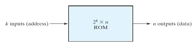
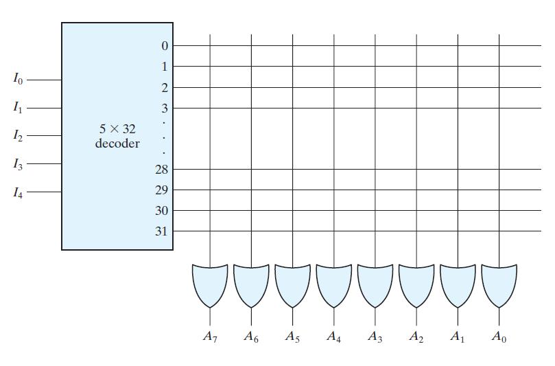
20 ROM (Read-Only Memory) k = 5, n = 8
21 Programming Rom According to Table 1 0
22 Read-Only Memory Cells BL BL BL 1 WL WL V DD WL BL BL BL 0 WL WL WL GND Diode ROM MOS ROM 1 MOS ROM 2
23 Read-Only Memory: MOS-NOR ROM V DD Pull-up devices WL[0] WL [1] GND WL [2] GND WL [3] BL [0] BL [1] BL [2] BL [3]
24 Read-Only Memory: Mask Programming Cell (9.5λ x 7λ) Programming using the Active Layer Only Polysilicon Metal1 GND Line Metal1 on Diffusion Vender should prepare customized mask (expensive)
25 Read-Only Memory: Contact Programming (PROM) Cell (11λ x 7λ) Programmming using the Contact Layer Only Inact fuse will be removed by high field Polysilicon Metal1 GND Line Metal1 on Diffusion
26 Memory Classification based on functionality ROM : Read-Only Memory RWM : Read-Write Memory RWM NVRWM ROM Random Access Memory (RAM) Non-Random Access SRAM DRAM FIFO LIFO Register CAM EPROM EEPROM FLASH PROM
27 Flash Memory Source Floating gate Gate Drain D t ox G n + Substrate p t ox n +_ S 20 V Device cross-section 0 V Schematic symbol 5 V 10 V 5 V 20 V -5 V 0 V V 5 V S D S D S D Tunneling injection 27 Removing programming voltage leaves charge trapped Programming results in higher V T.

28 Programmable Logic Device (PLD)
29 Programmable Logic Array Programmable AND array Programmable OR array F1=AB + AC + A BC F2= (AC + BC)
30 Programmable Array Logic PAL-With a fixed OR array and a programmable AND array. Not as flexible as the PLA (Only the AND gate are programmable.)
31 Programmable Array Logic: Example wabcd (,,, ) = (2,12,13) xabcd (,,, ) = (7,8,9,10,11,12,12,14,15) yabcd (,,, ) = (0, 2, 3, 4, 5, 6, 7,8,10,11,15) z( ABCD,,, ) = (1, 2,8,12,13,) K-Map w = ABC ' + A' B ' CD ' x = A + BCD y = A' B + CD + B ' D ' z = ABC ' + A' B ' CD ' + AC ' D ' + A' B ' C ' D = w+ ACD ' ' + ABCD ' ' '
32 Programmable Array Logic: Example (Cont.)
33 Sequential Programmable Devices Sequential (or simple) Programmable Logic Device (SPLD) Complex Programmable Logic Device (CPLD) Field Programmable Gate Array (FPGA) + Unlike combinational PLD s, includes both gates and flipflops
 Basic Macro-cell Logic")
34 Sequential Programmable Logic Device Sequential Programmable Logic Device (SPLD) Basic Macro-cell Logic of SPLD

35 Complex Programmable Logic Device Multiple PLD s are interconnected through a programmable switch matrix
36 Field Programmable Gate Array Look up table A truth table stored in SRAM, which provides the combinational circuit functions Multiplexers / Gates / Flip-flops Example: Xilinx, Altera

37 Xilinx Spartan : Basic Architecture The loop up table of CLB can be utilized as block memory

38 Xilinx Spartan : Programmable Interconnect Point PIP = transmission gate whose is controlled by SRAM cell
39 Xilinx Spartan : I/O Blocks (IOB) IOB s are bi-directional The output buffer should be implemented as tri-gates


40 Xilinx Spartan : Distributed RAM Single-Port RAM CLB is able to form single-port / dual-port RAM dual-port RAM

41 Xilinx Spartan ΙΙ Architecture

42 Xilinx FPGA
Memory and Programmable Logic
 Memory and Programmable Logic Memory units allow us to store and/or retrieve information Essentially look-up tables Good for storing data, not for function implementation Programmable logic device (PLD),
Integrated Circuits & Systems
 Federal University of Santa Catarina Center for Technology Computer Science & Electronics Engineering Integrated Circuits & Systems INE 5442 Lecture 23-1 guntzel@inf.ufsc.br Semiconductor Memory Classification
Presentation 4: Programmable Combinational Devices
 Presentation 4: Programmable Combinational Devices Asst. Prof Dr. Ahmet ÖZKURT DEUEEE Based on the Presentation by Prof. Kim, Young Ho Dept. of Information Computer Engineering E-mail : yhkim@hyowon.cs.pusan.ac.kr
Memory and Programmable Logic
 Memory and Programmable Logic Mano & Ciletti Chapter 7 By Suleyman TOSUN Ankara University Outline RAM Memory decoding Error detection and correction ROM Programmable Logic Array (PLA) Programmable Array
CMPEN 411 VLSI Digital Circuits Spring Lecture 22: Memery, ROM
 CMPEN 411 VLSI Digital Circuits Spring 2011 Lecture 22: Memery, ROM [Adapted from Rabaey s Digital Integrated Circuits, Second Edition, 2003 J. Rabaey, A. Chandrakasan, B. Nikolic] Sp11 CMPEN 411 L22 S.1
PROGRAMMABLE MODULES SPECIFICATION OF PROGRAMMABLE COMBINATIONAL AND SEQUENTIAL MODULES
 PROGRAMMABLE MODULES SPECIFICATION OF PROGRAMMABLE COMBINATIONAL AND SEQUENTIAL MODULES. psa. rom. fpga THE WAY THE MODULES ARE PROGRAMMED NETWORKS OF PROGRAMMABLE MODULES EXAMPLES OF USES Programmable
ELCT 912: Advanced Embedded Systems
 Advanced Embedded Systems Lecture 2: Memory and Programmable Logic Dr. Mohamed Abd El Ghany, Memory Random Access Memory (RAM) Can be read and written Static Random Access Memory (SRAM) Data stored so
Magnetic core memory (1951) cm 2 ( bit)
 cm 2 ( bit)") Magnetic core memory (1951) 16 16 cm 2 (128 128 bit) Semiconductor Memory Classification Read-Write Memory Non-Volatile Read-Write Memory Read-Only Memory Random Access Non-Random Access EPROM E 2 PROM
Magnetic core memory (1951) 16 16 cm 2 (128 128 bit) Semiconductor Memory Classification Read-Write Memory Non-Volatile Read-Write Memory Read-Only Memory Random Access Non-Random Access EPROM E 2 PROM
Lecture 13: Memory and Programmable Logic
 Lecture 13: Memory and Programmable Logic Syed M. Mahmud, Ph.D ECE Department Wayne State University Aby K George, ECE Department, Wayne State University Contents Introduction Random Access Memory Memory
COMP3221: Microprocessors and. and Embedded Systems. Overview. Lecture 23: Memory Systems (I)
") COMP3221: Microprocessors and Embedded Systems Lecture 23: Memory Systems (I) Overview Memory System Hierarchy RAM, ROM, EPROM, EEPROM and FLASH http://www.cse.unsw.edu.au/~cs3221 Lecturer: Hui Wu Session
COMP3221: Microprocessors and Embedded Systems Lecture 23: Memory Systems (I) Overview Memory System Hierarchy RAM, ROM, EPROM, EEPROM and FLASH http://www.cse.unsw.edu.au/~cs3221 Lecturer: Hui Wu Session
MEMORY AND PROGRAMMABLE LOGIC
 MEMORY AND PROGRAMMABLE LOGIC Memory is a device where we can store and retrieve information It can execute a read and a write Programmable Logic is a device where we can store and retrieve information
ESE370: Circuit-Level Modeling, Design, and Optimization for Digital Systems
 ESE370: Circuit-Level Modeling, Design, and Optimization for Digital Systems Lec 26: November 9, 2018 Memory Overview Dynamic OR4! Precharge time?! Driving input " With R 0 /2 inverter! Driving inverter
Programmable Logic Devices UNIT II DIGITAL SYSTEM DESIGN
 Programmable Logic Devices UNIT II DIGITAL SYSTEM DESIGN 2 3 4 5 6 7 8 9 2 3 4 5 6 7 8 9 2 Implementation in Sequential Logic 2 PAL Logic Implementation Design Example: BCD to Gray Code Converter A B
! Memory Overview. ! ROM Memories. ! RAM Memory " SRAM " DRAM. ! This is done because we can build. " large, slow memories OR
 ESE 57: Digital Integrated Circuits and VLSI Fundamentals Lec 2: April 5, 26 Memory Overview, Memory Core Cells Lecture Outline! Memory Overview! ROM Memories! RAM Memory " SRAM " DRAM 2 Memory Overview
CHAPTER 9 MULTIPLEXERS, DECODERS, AND PROGRAMMABLE LOGIC DEVICES
 CHAPTER 9 MULTIPLEXERS, DECODERS, AND PROGRAMMABLE LOGIC DEVICES This chapter in the book includes: Objectives Study Guide 9.1 Introduction 9.2 Multiplexers 9.3 Three-State Buffers 9.4 Decoders and Encoders
Hardware Design with VHDL PLDs I ECE 443. FPGAs can be configured at least once, many are reprogrammable.
 PLDs, ASICs and FPGAs FPGA definition: Digital integrated circuit that contains configurable blocks of logic and configurable interconnects between these blocks. Key points: Manufacturer does NOT determine
Programmable Logic Devices
 Programmable Logic Devices Programmable Logic Devices Fig. (1) General structure of PLDs Programmable Logic Device (PLD): is an integrated circuit with internal logic gates and/or connections that can
Computer Structure. Unit 2: Memory and programmable devices
 Computer Structure Unit 2: Memory and programmable devices Translated from Francisco Pérez García (fperez at us.es) by Mª Carmen Romero (mcromerot at us.es, Office G1.51, 954554324) Electronic Technology
Semiconductor Memory Classification. Today. ESE 570: Digital Integrated Circuits and VLSI Fundamentals. CPU Memory Hierarchy.
 ESE 57: Digital Integrated Circuits and VLSI Fundamentals Lec : April 4, 7 Memory Overview, Memory Core Cells Today! Memory " Classification " ROM Memories " RAM Memory " Architecture " Memory core " SRAM
CMPE 415 Programmable Logic Devices FPGA Technology I
 Department of Computer Science and Electrical Engineering CMPE 415 Programmable Logic Devices FPGA Technology I Prof. Ryan Robucci Some slides (blue-frame) developed by Jim Plusquellic Some images credited
Semiconductor Memory Classification
 ESE37: Circuit-Level Modeling, Design, and Optimization for Digital Systems Lec 6: November, 7 Memory Overview Today! Memory " Classification " Architecture " Memory core " Periphery (time permitting)!
Topics. Midterm Finish Chapter 7
 Lecture 9 Topics Midterm Finish Chapter 7 ROM (review) Memory device in which permanent binary information is stored. Example: 32 x 8 ROM Five input lines (2 5 = 32) 32 outputs, each representing a memory
Evolution of Implementation Technologies. ECE 4211/5211 Rapid Prototyping with FPGAs. Gate Array Technology (IBM s) Programmable Logic
 Programmable Logic") ECE 42/52 Rapid Prototyping with FPGAs Dr. Charlie Wang Department of Electrical and Computer Engineering University of Colorado at Colorado Springs Evolution of Implementation Technologies Discrete devices:
ECE 42/52 Rapid Prototyping with FPGAs Dr. Charlie Wang Department of Electrical and Computer Engineering University of Colorado at Colorado Springs Evolution of Implementation Technologies Discrete devices:
Unit 6 1.Random Access Memory (RAM) Chapter 3 Combinational Logic Design 2.Programmable Logic
 Chapter 3 Combinational Logic Design 2.Programmable Logic") EE 200: Digital Logic Circuit Design Dr Radwan E Abdel-Aal, COE Unit 6.Random Access Memory (RAM) Chapter 3 Combinational Logic Design 2. Logic Logic and Computer Design Fundamentals Part Implementation
EE 200: Digital Logic Circuit Design Dr Radwan E Abdel-Aal, COE Unit 6.Random Access Memory (RAM) Chapter 3 Combinational Logic Design 2. Logic Logic and Computer Design Fundamentals Part Implementation
+1 (479)
") Memory Courtesy of Dr. Daehyun Lim@WSU, Dr. Harris@HMC, Dr. Shmuel Wimer@BIU and Dr. Choi@PSU http://csce.uark.edu +1 (479) 575-6043 yrpeng@uark.edu Memory Arrays Memory Arrays Random Access Memory Serial
Memory Courtesy of Dr. Daehyun Lim@WSU, Dr. Harris@HMC, Dr. Shmuel Wimer@BIU and Dr. Choi@PSU http://csce.uark.edu +1 (479) 575-6043 yrpeng@uark.edu Memory Arrays Memory Arrays Random Access Memory Serial
Fig. 6-1 Conventional and Array Logic Symbols for OR Gate
 6- (a) Conventional symbol (b) Array logic symbol Fig. 6- Conventional and Array Logic Symbols for OR Gate 2 Prentice Hall, Inc. 6-2 k address lines Read n data input lines emory unit 2 k words n bits
CHAPTER 12 ARRAY SUBSYSTEMS [ ] MANJARI S. KULKARNI
![CHAPTER 12 ARRAY SUBSYSTEMS [ ] MANJARI S. KULKARNI](/thumbs/76/73997056.jpg "CHAPTER 12 ARRAY SUBSYSTEMS [ ] MANJARI S. KULKARNI") CHAPTER 2 ARRAY SUBSYSTEMS [2.4-2.9] MANJARI S. KULKARNI OVERVIEW Array classification Non volatile memory Design and Layout Read-Only Memory (ROM) Pseudo nmos and NAND ROMs Programmable ROMS PROMS, EPROMs,
CHAPTER 2 ARRAY SUBSYSTEMS [2.4-2.9] MANJARI S. KULKARNI OVERVIEW Array classification Non volatile memory Design and Layout Read-Only Memory (ROM) Pseudo nmos and NAND ROMs Programmable ROMS PROMS, EPROMs,
Very Large Scale Integration (VLSI)
") Very Large Scale Integration (VLSI) Lecture 6 Dr. Ahmed H. Madian Ah_madian@hotmail.com Dr. Ahmed H. Madian-VLSI 1 Contents FPGA Technology Programmable logic Cell (PLC) Mux-based cells Look up table PLA
Very Large Scale Integration (VLSI) Lecture 6 Dr. Ahmed H. Madian Ah_madian@hotmail.com Dr. Ahmed H. Madian-VLSI 1 Contents FPGA Technology Programmable logic Cell (PLC) Mux-based cells Look up table PLA
Very Large Scale Integration (VLSI)
") Very Large Scale Integration (VLSI) Lecture 8 Dr. Ahmed H. Madian ah_madian@hotmail.com Content Array Subsystems Introduction General memory array architecture SRAM (6-T cell) CAM Read only memory Introduction
Very Large Scale Integration (VLSI) Lecture 8 Dr. Ahmed H. Madian ah_madian@hotmail.com Content Array Subsystems Introduction General memory array architecture SRAM (6-T cell) CAM Read only memory Introduction
DIGITAL CIRCUIT LOGIC UNIT 9: MULTIPLEXERS, DECODERS, AND PROGRAMMABLE LOGIC DEVICES
 DIGITAL CIRCUIT LOGIC UNIT 9: MULTIPLEXERS, DECODERS, AND PROGRAMMABLE LOGIC DEVICES 1 Learning Objectives 1. Explain the function of a multiplexer. Implement a multiplexer using gates. 2. Explain the
ELCT 501: Digital System Design
 ELCT 501: Digital System Lecture 3: Memory and Programmable Logic (continue) Dr. Mohamed Abd El Ghany, Memory Model 32-bit address space can address up to 4 GB (2 32 ) different memory locations 0x00000000
Memory. Outline. ECEN454 Digital Integrated Circuit Design. Memory Arrays. SRAM Architecture DRAM. Serial Access Memories ROM
 ECEN454 Digital Integrated Circuit Design Memory ECEN 454 Memory Arrays SRAM Architecture SRAM Cell Decoders Column Circuitry Multiple Ports DRAM Outline Serial Access Memories ROM ECEN 454 12.2 1 Memory
PROGRAMMABLE LOGIC DEVICES
 PROGRAMMABLE LOGIC DEVICES Programmable logic devices (PLDs) are used for designing logic circuits. PLDs can be configured by the user to perform specific functions. The different types of PLDs available
Outline. Field Programmable Gate Arrays. Programming Technologies Architectures. Programming Interfaces. Historical perspective
 Outline Field Programmable Gate Arrays Historical perspective Programming Technologies Architectures PALs, PLDs,, and CPLDs FPGAs Programmable logic Interconnect network I/O buffers Specialized cores Programming
Section 6. Memory Components Chapter 5.7, 5.8 Physical Implementations Chapter 7 Programmable Processors Chapter 8
 Section 6 Memory Components Chapter 5.7, 5.8 Physical Implementations Chapter 7 Programmable Processors Chapter 8 Types of memory Two major types of memory Volatile When power to the device is removed
FPGA for Complex System Implementation. National Chiao Tung University Chun-Jen Tsai 04/14/2011
 FPGA for Complex System Implementation National Chiao Tung University Chun-Jen Tsai 04/14/2011 About FPGA FPGA was invented by Ross Freeman in 1989 SRAM-based FPGA properties Standard parts Allowing multi-level
Design with Microprocessors
 Design with Microprocessors Year III Computer Sci. English 1-st Semester Lecture 12: Memory interfacing Typical Memory Hierarchy [1] On-Chip Components Control edram Datapath RegFile ITLB DTLB Instr Data
Based on slides/material by. Topic 7-4. Memory and Array Circuits. Outline. Semiconductor Memory Classification
 Based on slides/material by Topic 7 Memory and Array Circuits K. Masselos http://cas.ee.ic.ac.uk/~kostas J. Rabaey http://bwrc.eecs.berkeley.edu/classes/icbook/instructors.html Digital Integrated Circuits:
Programmable Logic Devices Introduction CMPE 415. Programmable Logic Devices
 Instructor: Professor Jim Plusquellic Programmable Logic Devices Text: The Design Warrior s Guide to FPGAs, Devices, Tools and Flows, Clive "Max" Maxfield, ISBN: 0-7506-7604-3 Modeling, Synthesis and Rapid
CONTENTS CHAPTER 1: NUMBER SYSTEM. Foreword...(vii) Preface... (ix) Acknowledgement... (xi) About the Author...(xxiii)
 Preface... (ix) Acknowledgement... (xi) About the Author...(xxiii)") CONTENTS Foreword...(vii) Preface... (ix) Acknowledgement... (xi) About the Author...(xxiii) CHAPTER 1: NUMBER SYSTEM 1.1 Digital Electronics... 1 1.1.1 Introduction... 1 1.1.2 Advantages of Digital Systems...
CONTENTS Foreword...(vii) Preface... (ix) Acknowledgement... (xi) About the Author...(xxiii) CHAPTER 1: NUMBER SYSTEM 1.1 Digital Electronics... 1 1.1.1 Introduction... 1 1.1.2 Advantages of Digital Systems...
LSN 6 Programmable Logic Devices
 LSN 6 Programmable Logic Devices Department of Engineering Technology LSN 6 What Are PLDs? Functionless devices in base form Require programming to operate The logic function of the device is programmed
Embedded Controller Design. CompE 270 Digital Systems - 5. Objective. Application Specific Chips. User Programmable Logic. Copyright 1998 Ken Arnold 1
 CompE 270 Digital Systems - 5 Programmable Logic Ken Arnold Objective Application Specific ICs Introduce User Programmable Logic Common Architectures Programmable Array Logic Address Decoding Example Development
CENG 4480 L09 Memory 3
 CENG 4480 L09 Memory 3 Bei Yu Chapter 11 Memories Reference: CMOS VLSI Design A Circuits and Systems Perspective by H.E.Weste and D.M.Harris 1 Memory Arrays Memory Arrays Random Access Memory Serial Access
Semiconductor Memories: RAMs and ROMs
 Semiconductor Memories: RAMs and ROMs Lesson Objectives: In this lesson you will be introduced to: Different memory devices like, RAM, ROM, PROM, EPROM, EEPROM, etc. Different terms like: read, write,
Design with Microprocessors
 Design with Microprocessors Year III Computer Sci. English 1-st Semester Lecture 12: Memory interfacing Typical Memory Hierarchy [1] On-Chip Components Control edram Datapath RegFile ITLB DTLB Instr Data
UNIT - V MEMORY P.VIDYA SAGAR ( ASSOCIATE PROFESSOR) Department of Electronics and Communication Engineering, VBIT
 Department of Electronics and Communication Engineering, VBIT") UNIT - V MEMORY P.VIDYA SAGAR ( ASSOCIATE PROFESSOR) contents Memory: Introduction, Random-Access memory, Memory decoding, ROM, Programmable Logic Array, Programmable Array Logic, Sequential programmable
UNIT - V MEMORY P.VIDYA SAGAR ( ASSOCIATE PROFESSOR) contents Memory: Introduction, Random-Access memory, Memory decoding, ROM, Programmable Logic Array, Programmable Array Logic, Sequential programmable
UMBC. Select. Read. Write. Output/Input-output connection. 1 (Feb. 25, 2002) Four commonly used memories: Address connection ... Dynamic RAM (DRAM)
 Four commonly used memories: Address connection ... Dynamic RAM (DRAM)") Memory Types Two basic types: ROM: Read-only memory RAM: Read-Write memory Four commonly used memories: ROM Flash (EEPROM) Static RAM (SRAM) Dynamic RAM (DRAM) Generic pin configuration: Address connection
Memory Types Two basic types: ROM: Read-only memory RAM: Read-Write memory Four commonly used memories: ROM Flash (EEPROM) Static RAM (SRAM) Dynamic RAM (DRAM) Generic pin configuration: Address connection
FPGA Programming Technology
 FPGA Programming Technology Static RAM: This Xilinx SRAM configuration cell is constructed from two cross-coupled inverters and uses a standard CMOS process. The configuration cell drives the gates of
CENG 4480 L09 Memory 2
 CENG 4480 L09 Memory 2 Bei Yu Reference: Chapter 11 Memories CMOS VLSI Design A Circuits and Systems Perspective by H.E.Weste and D.M.Harris 1 v.s. CENG3420 CENG3420: architecture perspective memory coherent
UNIT V (PROGRAMMABLE LOGIC DEVICES)
") UNIT V (PROGRAMMABLE LOGIC DEVICES) Introduction There are two types of memories that are used in digital systems: Random-access memory(ram): perform both the write and read operations. Read-only memory(rom):
UNIT V (PROGRAMMABLE LOGIC DEVICES) Introduction There are two types of memories that are used in digital systems: Random-access memory(ram): perform both the write and read operations. Read-only memory(rom):
EECS150 - Digital Design Lecture 16 Memory 1
 EECS150 - Digital Design Lecture 16 Memory 1 March 13, 2003 John Wawrzynek Spring 2003 EECS150 - Lec16-mem1 Page 1 Memory Basics Uses: Whenever a large collection of state elements is required. data &
ECE 485/585 Microprocessor System Design
 Microprocessor System Design Lecture 4: Memory Hierarchy Memory Taxonomy SRAM Basics Memory Organization DRAM Basics Zeshan Chishti Electrical and Computer Engineering Dept Maseeh College of Engineering
EECS150 - Digital Design Lecture 16 - Memory
 EECS150 - Digital Design Lecture 16 - Memory October 17, 2002 John Wawrzynek Fall 2002 EECS150 - Lec16-mem1 Page 1 Memory Basics Uses: data & program storage general purpose registers buffering table lookups
FPGA. Logic Block. Plessey FPGA: basic building block here is 2-input NAND gate which is connected to each other to implement desired function.
 FPGA Logic block of an FPGA can be configured in such a way that it can provide functionality as simple as that of transistor or as complex as that of a microprocessor. It can used to implement different
Organization. 5.1 Semiconductor Main Memory. William Stallings Computer Organization and Architecture 6th Edition
 William Stallings Computer Organization and Architecture 6th Edition Chapter 5 Internal Memory 5.1 Semiconductor Main Memory 5.2 Error Correction 5.3 Advanced DRAM Organization 5.1 Semiconductor Main Memory
PLAs & PALs. Programmable Logic Devices (PLDs) PLAs and PALs
 PLAs and PALs") PLAs & PALs Programmable Logic Devices (PLDs) PLAs and PALs PLAs&PALs By the late 1970s, standard logic devices were all the rage, and printed circuit boards were loaded with them. To offer the ultimate
PLAs & PALs Programmable Logic Devices (PLDs) PLAs and PALs PLAs&PALs By the late 1970s, standard logic devices were all the rage, and printed circuit boards were loaded with them. To offer the ultimate
Concept of Memory. The memory of computer is broadly categories into two categories:
 Concept of Memory We have already mentioned that digital computer works on stored programmed concept introduced by Von Neumann. We use memory to store the information, which includes both program and data.
I 4 I 3 I 2 I 1 I 0 A 7 A 6 A 5 A 4 A 3 A 2 A 1 A 0 T-125. ROM Truth Table (Partial) 1997 by Prentice-Hall, Inc.
 1997 by Prentice-Hall, Inc.") 997 by Prentice-Hall, Inc. ano & Kime Upper Saddle River, New Jersey 7458 T-5 Inputs Outputs I 4 I 3 I I I A 7 A 6 A 5 A 4 A 3 A A A...... RO Truth Table (Partial) 997 by Prentice-Hall, Inc. ano & Kime
997 by Prentice-Hall, Inc. ano & Kime Upper Saddle River, New Jersey 7458 T-5 Inputs Outputs I 4 I 3 I I I A 7 A 6 A 5 A 4 A 3 A A A...... RO Truth Table (Partial) 997 by Prentice-Hall, Inc. ano & Kime
Design Methodologies. Full-Custom Design
 Design Methodologies Design styles Full-custom design Standard-cell design Programmable logic Gate arrays and field-programmable gate arrays (FPGAs) Sea of gates System-on-a-chip (embedded cores) Design
Chapter 13 Programmable Logic Device Architectures
 Chapter 13 Programmable Logic Device Architectures Chapter 13 Objectives Selected areas covered in this chapter: Describing different categories of digital system devices. Describing different types of
Memory in Digital Systems
 MEMORIES Memory in Digital Systems Three primary components of digital systems Datapath (does the work) Control (manager) Memory (storage) Single bit ( foround ) Clockless latches e.g., SR latch Clocked
Digital Integrated Circuits
 Digital Integrated Circuits Lecture 9 Jaeyong Chung Robust Systems Laboratory Incheon National University DIGITAL DESIGN FLOW Chung EPC6055 2 FPGA vs. ASIC FPGA (A programmable Logic Device) Faster time-to-market
Microcontroller Systems. ELET 3232 Topic 11: General Memory Interfacing
 Microcontroller Systems ELET 3232 Topic 11: General Memory Interfacing 1 Objectives To become familiar with the concepts of memory expansion and the data and address bus To design embedded systems circuits
Introduction to SRAM. Jasur Hanbaba
 Introduction to SRAM Jasur Hanbaba Outline Memory Arrays SRAM Architecture SRAM Cell Decoders Column Circuitry Non-volatile Memory Manufacturing Flow Memory Arrays Memory Arrays Random Access Memory Serial
Digital Design, Kyung Hee Univ. Chapter 7. Memory and Programmable Logic
 Chapter 7. Memory and Programmable Logic 1 7.1 Introduction Memory unit: A device to which binary information is transferred for storage and from which information is retrieved when needed for processing
CMOS Logic Circuit Design Link( リンク ): センター教官講義ノートの下 CMOS 論理回路設計
: センター教官講義ノートの下 CMOS 論理回路設計") CMOS Logic Circuit Design http://www.rcns.hiroshima-u.ac.jp Link( リンク ): センター教官講義ノートの下 CMOS 論理回路設計 Memory Circuits (Part 1) Overview of Memory Types Memory with Address-Based Access Principle of Data Access
CMOS Logic Circuit Design http://www.rcns.hiroshima-u.ac.jp Link( リンク ): センター教官講義ノートの下 CMOS 論理回路設計 Memory Circuits (Part 1) Overview of Memory Types Memory with Address-Based Access Principle of Data Access
Memory in Digital Systems
 MEMORIES Memory in Digital Systems Three primary components of digital systems Datapath (does the work) Control (manager) Memory (storage) Single bit ( foround ) Clockless latches e.g., SR latch Clocked
FPGA Implementations
 FPGA Implementations Smith Text: Chapters 4-8 Online version at: http://www10.edacafe.com/book/asic/asics.php Topic outline Chapter 4 Programmable ASIC technologies Chapter 5 Programmable logic cells Chapter
Lecture 13: SRAM. Slides courtesy of Deming Chen. Slides based on the initial set from David Harris. 4th Ed.
 Lecture 13: SRAM Slides courtesy of Deming Chen Slides based on the initial set from David Harris CMOS VLSI Design Outline Memory Arrays SRAM Architecture SRAM Cell Decoders Column Circuitry Multiple Ports
Lecture 11 SRAM Zhuo Feng. Z. Feng MTU EE4800 CMOS Digital IC Design & Analysis 2010
 EE4800 CMOS Digital IC Design & Analysis Lecture 11 SRAM Zhuo Feng 11.1 Memory Arrays SRAM Architecture SRAM Cell Decoders Column Circuitryit Multiple Ports Outline Serial Access Memories 11.2 Memory Arrays
William Stallings Computer Organization and Architecture 6th Edition. Chapter 5 Internal Memory
 William Stallings Computer Organization and Architecture 6th Edition Chapter 5 Internal Memory Semiconductor Memory Types Semiconductor Memory RAM Misnamed as all semiconductor memory is random access
END-TERM EXAMINATION
 (Please Write your Exam Roll No. immediately) END-TERM EXAMINATION DECEMBER 2006 Exam. Roll No... Exam Series code: 100919DEC06200963 Paper Code: MCA-103 Subject: Digital Electronics Time: 3 Hours Maximum
Motivation for Lecture. Market for Memories. Example: FFT Design. Sequential Circuits & D flip-flop. Latches and Registers.
 Motivation for Lecture Design Methodologies Storage (registers and memories) Computational platforms Design Methodologies Memories is a crucial part of most designs: What different type of memories are
ECE 331 Digital System Design
 ECE 331 Digital System Design Tristate Buffers, Read-Only Memories and Programmable Logic Devices (Lecture #17) The slides included herein were taken from the materials accompanying Fundamentals of Logic
Read and Write Cycles
 Read and Write Cycles The read cycle is shown. Figure 41.1a. The RAS and CAS signals are activated one after the other to latch the multiplexed row and column addresses respectively applied at the multiplexed
EE141-Fall 2007 Digital Integrated Circuits. ROM and Flash. Announcements. Read-Only Memory Cells. Class Material. Semiconductor Memory Classification
 EE4-Fall 2007 igital Integrated Circuits Lecture 29 ROM, Flash, and RAM ROM and Flash 4 4 Announcements Final ec. 20 th Room TBA Final review sessions: Mon. ec. 7 th 3:30pm, 550 Cory Tues. ec. 7 th 3:30pm,
Sense Amplifiers 6 T Cell. M PC is the precharge transistor whose purpose is to force the latch to operate at the unstable point.
 Announcements (Crude) notes for switching speed example from lecture last week posted. Schedule Final Project demo with TAs. Written project report to include written evaluation section. Send me suggestions
Chapter 3 Semiconductor Memories. Jin-Fu Li Department of Electrical Engineering National Central University Jungli, Taiwan
 Chapter 3 Semiconductor Memories Jin-Fu Li Department of Electrical Engineering National Central University Jungli, Taiwan Outline Introduction Random Access Memories Content Addressable Memories Read
Basic Organization Memory Cell Operation. CSCI 4717 Computer Architecture. ROM Uses. Random Access Memory. Semiconductor Memory Types
 CSCI 4717/5717 Computer Architecture Topic: Internal Memory Details Reading: Stallings, Sections 5.1 & 5.3 Basic Organization Memory Cell Operation Represent two stable/semi-stable states representing
DIGITAL SYSTEM FUNDAMENTALS (ECE421) DIGITAL ELECTRONICS FUNDAMENTAL (ECE4220. PROGRAMMABLE LOGIC DEVICES (PLDs)
 DIGITAL ELECTRONICS FUNDAMENTAL (ECE4220. PROGRAMMABLE LOGIC DEVICES (PLDs)") COURSE / CODE DIGITAL SYSTEM FUNDAMENTALS (ECE421) DIGITAL ELECTRONICS FUNDAMENTAL (ECE4220 PROGRAMMABLE LOGIC DEVICES (PLDs) A PLD, or programmable logic device, is an electronic component that is used
COURSE / CODE DIGITAL SYSTEM FUNDAMENTALS (ECE421) DIGITAL ELECTRONICS FUNDAMENTAL (ECE4220 PROGRAMMABLE LOGIC DEVICES (PLDs) A PLD, or programmable logic device, is an electronic component that is used
Digital Systems. Semiconductor memories. Departamentul de Bazele Electronicii
 Digital Systems Semiconductor memories Departamentul de Bazele Electronicii Outline ROM memories ROM memories PROM memories EPROM memories EEPROM, Flash, MLC memories Applications with ROM memories extending
Digital Integrated Circuits (83-313) Lecture 7: SRAM. Semester B, Lecturer: Dr. Adam Teman Itamar Levi, Robert Giterman.
 Lecture 7: SRAM. Semester B, Lecturer: Dr. Adam Teman Itamar Levi, Robert Giterman.") Digital Integrated Circuits (83-313) Lecture 7: SRAM Semester B, 2016-17 Lecturer: Dr. Adam Teman TAs: Itamar Levi, Robert Giterman 16 May 2017 Disclaimer: This course was prepared, in its entirety, by
Digital Integrated Circuits (83-313) Lecture 7: SRAM Semester B, 2016-17 Lecturer: Dr. Adam Teman TAs: Itamar Levi, Robert Giterman 16 May 2017 Disclaimer: This course was prepared, in its entirety, by
SRAM. Introduction. Digital IC
 SRAM Introduction Outline Memory Arrays SRAM Architecture SRAM Cell Decoders Column Circuitry Multiple Ports Serial Access Memories Memory Arrays Memory Arrays Random Access Memory Serial Access Memory
Memory & Simple I/O Interfacing
 Chapter 10 Memory & Simple I/O Interfacing Expected Outcomes Explain the importance of tri-state devices in microprocessor system Distinguish basic type of semiconductor memory and their applications Relate
ECE 636. Reconfigurable Computing. Lecture 2. Field Programmable Gate Arrays I
 ECE 636 Reconfigurable Computing Lecture 2 Field Programmable Gate Arrays I Overview Anti-fuse and EEPROM-based devices Contemporary SRAM devices - Wiring - Embedded New trends - Single-driver wiring -
P-2 Digital Design & Applications
 P-2 Digital Design & Applications Semiconductor Memory (Unit-V) By: A K Verma SOS in Electronics & Photonics Pt. Ravishankar Shukla University, Raipur (C.G.) 1 What is Memory? In computing, memory refers
Memory Design I. Array-Structured Memory Architecture. Professor Chris H. Kim. Dept. of ECE.
 Memory Design I Professor Chris H. Kim University of Minnesota Dept. of ECE chriskim@ece.umn.edu Array-Structured Memory Architecture 2 1 Semiconductor Memory Classification Read-Write Wi Memory Non-Volatile
Introduction to CMOS VLSI Design Lecture 13: SRAM
 Introduction to CMOS VLSI Design Lecture 13: SRAM David Harris Harvey Mudd College Spring 2004 1 Outline Memory Arrays SRAM Architecture SRAM Cell Decoders Column Circuitry Multiple Ports Serial Access
Computer Organization. 8th Edition. Chapter 5 Internal Memory
 William Stallings Computer Organization and Architecture 8th Edition Chapter 5 Internal Memory Semiconductor Memory Types Memory Type Category Erasure Write Mechanism Volatility Random-access memory (RAM)
(Advanced) Computer Organization & Architechture. Prof. Dr. Hasan Hüseyin BALIK (5 th Week)
 Computer Organization & Architechture. Prof. Dr. Hasan Hüseyin BALIK (5 th Week)") + (Advanced) Computer Organization & Architechture Prof. Dr. Hasan Hüseyin BALIK (5 th Week) + Outline 2. The computer system 2.1 A Top-Level View of Computer Function and Interconnection 2.2 Cache Memory
+ (Advanced) Computer Organization & Architechture Prof. Dr. Hasan Hüseyin BALIK (5 th Week) + Outline 2. The computer system 2.1 A Top-Level View of Computer Function and Interconnection 2.2 Cache Memory
Computer Organization and Assembly Language (CS-506)
") Computer Organization and Assembly Language (CS-506) Muhammad Zeeshan Haider Ali Lecturer ISP. Multan ali.zeeshan04@gmail.com https://zeeshanaliatisp.wordpress.com/ Lecture 2 Memory Organization and Structure
Computer Organization and Assembly Language (CS-506) Muhammad Zeeshan Haider Ali Lecturer ISP. Multan ali.zeeshan04@gmail.com https://zeeshanaliatisp.wordpress.com/ Lecture 2 Memory Organization and Structure
FYSE420 DIGITAL ELECTRONICS. Lecture 7
 FYSE420 DIGITAL ELECTRONICS Lecture 7 1 [1] [2] [3] DIGITAL LOGIC CIRCUIT ANALYSIS & DESIGN Nelson, Nagle, Irvin, Carrol ISBN 0-13-463894-8 DIGITAL DESIGN Morris Mano Fourth edition ISBN 0-13-198924-3
Programmable Logic Devices (PLDs)
") Programmable Logic Devices (PLDs) 212: Digital Design I, week 13 PLDs basically store binary information in a volatile/nonvolatile device. Data is specified by designer and physically inserted (Programmed)
Programmable Logic Devices (PLDs) 212: Digital Design I, week 13 PLDs basically store binary information in a volatile/nonvolatile device. Data is specified by designer and physically inserted (Programmed)
Digital Integrated Circuits Lecture 13: SRAM
 Digital Integrated Circuits Lecture 13: SRAM Chih-Wei Liu VLSI Signal Processing LAB National Chiao Tung University cwliu@twins.ee.nctu.edu.tw DIC-Lec13 cwliu@twins.ee.nctu.edu.tw 1 Outline Memory Arrays
Code No: 07A3EC03 Set No. 1
 Code No: 07A3EC03 Set No. 1 II B.Tech I Semester Regular Examinations, November 2008 SWITCHING THEORY AND LOGIC DESIGN ( Common to Electrical & Electronic Engineering, Electronics & Instrumentation Engineering,
Digital Logic & Computer Design CS Professor Dan Moldovan Spring 2010
 Digital Logic & Computer Design CS 434 Professor Dan Moldovan Spring 2 Copyright 27 Elsevier 5- Chapter 5 :: Digital Building Blocks Digital Design and Computer Architecture David Money Harris and Sarah
SECTION-A
 M.Sc(CS) ( First Semester) Examination,2013 Digital Electronics Paper: Fifth ------------------------------------------------------------------------------------- SECTION-A I) An electronics circuit/ device
Design Methodologies
 Design Methodologies 1981 1983 1985 1987 1989 1991 1993 1995 1997 1999 2001 2003 2005 2007 2009 Complexity Productivity (K) Trans./Staff - Mo. Productivity Trends Logic Transistor per Chip (M) 10,000 0.1
Read-only memory Implementing logic with ROM Programmable logic devices Implementing logic with PLDs Static hazards
 Points Addressed in this Lecture Lecture 7: ROM Programmable Logic Devices Professor Peter Cheung Department of EEE, Imperial College London Read-only memory Implementing logic with ROM Programmable logic
Model EXAM Question Bank
 VELAMMAL COLLEGE OF ENGINEERING AND TECHNOLOGY, MADURAI Department of Information Technology Model Exam -1 1. List the main difference between PLA and PAL. PLA: Both AND and OR arrays are programmable