Parent page: PCB Panel
|
|
|
- Victor Dean
- 5 years ago
- Views:
Transcription
1 Published on Online Documentation for Altium Products ( 主页 > PCB Library Using Altium Documentation Modified by Annika Krilov on Apr 11, 2017 Parent page: PCB Panel
2
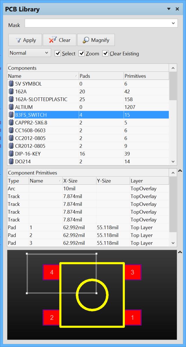
3 The PCB Library panel. Summary The PCB Library panel enables you to browse component footprints stored in the active PCB library document and edit their properties. When a PCB Library document is active, the panel becomes populated with information pertaining to the constituent footprints of that library. The panel also offers the ability to pass on any changes made to them directly to the PCB design document. Access To display the PCB Library panel, click the PCB button at the bottom-right of Altium Designer when the PCB Editor is active and select the PCB Library entry from the pop-up menu. Alternatively, you can access the panel through the View» Workspace Panels» PCB» PCB sub-menu. Panels can be configured to be floating in the editor space or docked to sides of the screen. If the PCB Library panel is currently in a group of panels, use the PCB Library tab located at the bottom of the panels to bring it to the front. Library Browsing The body of the PCB Library panel has three sections, each offering a different scope or view of the components in the active PCB Library: Components - The list of component footprints in the active library. The number of pads and primitive objects used to define the footprint is listed for each entry. Component Primitives - The primitive objects, and their main properties, that make up the currently selected component footprint. Mini-viewer window - A simplified, overall view of the currently selected component, with the main editor view indicated by an overlay graphic. As a component is selected in the PCB Library panel, its constituent primitives populate the Component Primitives section and the footprint is displayed in the main editor workspace. Selecting a primitive object in the panel causes the corresponding object to be highlighted in the editor workspace. In this way the PCB Library panel offers a fast and easy way to browse, view and access PCB library footprints.

4 A Pad primitive selected and highlighted from library component B3FS_SWITCH. Double-clicking on a Component entry opens the PCB Library Component dialog, and double-clicking on a Component Primitives entry will access its corresponding Properties dialog - see more options in the Right-Click section below. Filtering Content The contents of the list can be filtered, enabling you to quickly find a particular component footprint within the library. This is especially useful if the library contains a large number of items. Filtering can be applied using the following two methods: INDIRECT FILTERING This method uses the Mask field at the top of the panel to filter the contents of the list. Masking is applied based on the entry in the field. Only those components in the list targeted by the scope of the entry will remain displayed.

5 Note that the Mask field is not case sensitive. To list all component footprints again, clear (delete) the entry in the Mask field. Use the * wild card operator for more elaborate filtering. For example, typing m* will display only component footprints whose names begin with m. Or as in the image below, typing *16 will display only component footprints where the body of the name contains 16.
6 DIRECT FILTERING This method is available for all list regions in the panel and allows you to quickly jump to an entry by directly typing within the area of the list. Masking is not applied, leaving the full content of the list visible at all times. To use the feature for quickly finding a component footprint, click inside the Components section of the panel and type the first letter of the component footprint you wish to jump to. For example, if you wanted to quickly jump to component entries starting with the letter S, you would press that letter on the keyboard. The first component in the list starting with S would be made active, and the letter would be highlighted to indicate that filtering of the list is based upon it. If there are multiple components starting with the same letter and especially if the library is particularly large, type further letters to target the specific entry you require - for example; SOT as illustrated by image below.

7 To clear the current filtering, allowing you to enter a different starting letter, press Esc. Use the Backspace key to clear the previously entered filter characters in sequence. COMBINATION FILTERING In some situations it may be helpful to use Indirect and Direct filtering together. If, for example, you recall that the component you want to locate has a sub-type number of 4 and a prefix of PO, this information can be used as Indirect (Mask) and Direct entries respectively, as shown in the image below.
.")
8 Browsing Component Primitives The Component Primitives section of the panel lists all primitive objects that constitute the component footprint currently selected in the Components list. For each primitive entry, the following information is displayed: Type - the type of primitive object (e.g. pad, track, arc, etc). Name - the specified value for the objects' designator (where one exists). X-Size - the X dimension of the object (e.g. the width of an arc, track or fill; the X- Size value of a pad). Y-Size - the Y dimension of the object (e.g. the height of a fill; the Y-Size value of a pad. This field will be empty for a track or arc). Layer - the layer upon which the object resides.
 is graphically highlighted in the editor")
9 As individual object primitives are selected in the panel, the matching object (track, arc, pad, etc) is graphically highlighted in the editor workspace.
 applies a filter, essentially using the entry as")

10 CONTROLLING THE DISPLAY OF BROWSED ENTRIES IN THE WORKSPACE Selecting an entry in either panel list (Component or Primitives) applies a filter, essentially using the entry as its scope. The visual result of the applied filtering on the document in the design editor window is determined by a series of highlighting controls located at the top of the panel.

 objects, click the button at the bottom-right of the workspace: When this option is applied, unfiltered objects will be unavailable for")
11 Display functions Mask / Dim / Normal - this dropdown list provides the options for visibly contrasting filtered and unfiltered objects within the design editor window. The effectiveness of masking and dimming is determined by the Highlighting Options set in the PCB Editor - Display page of the Preferences dialog. When Mask is selected, filtered objects will appear visible in the design editor window, with all other objects being made monochrome. To set the contrast of the background (un-highlighted) objects, click the button at the bottom-right of the workspace: When this option is applied, unfiltered objects will be unavailable for selection or editing. When Dim is selected, filtered objects will appear visible in the design editor window, with all other objects retaining their colors, but being shaded. Set the balance between filtered and unfiltered objects using the Masked Objects Factor and Highlight Objects Factor sliders after clicking the button : Select - when enabled (default), the filtered objects will be selected in the workspace. Zoom - when enabled (default), the filtered objects will be zoomed and centered (where possible) in the design editor window. Clear Existing - when enabled (default), an existing filter will be cleared before applying a new one. Disabling this option allows you to extend an existing filter, essentially refining the filter further by applying a new filter in addition to the existing one. Any combination of these options can be enabled. For example, you might want to have all filtered objects zoomed, centered and selected in the design editor window, whilst applying masking to take away the clutter of other design objects. Use the Clear button to clear the currently-applied filter. All objects in the design workspace will become fully visible and available for selection/editing. If you wish to re-apply the filter, click on the Apply button. Using the Panel's Mini-viewer The bottom section of the panel provides a mini-viewer for the document, with an image of

12 the active component footprint central to its window. A white viewing box is imposed on the image, which represents the area currently displayed in the design editor window. As you pan around the document in the design editor window - either through use of the associated horizontal and vertical scrollbars or the right-click panning hand - the viewing box in the panel will move accordingly. Conversely, if you click inside the viewing box and drag it around the footprint image in the panel, the document in the design editor window will be panned accordingly, and at the current zoom level. As you zoom in or out in the design editor window, the viewing box will be resized accordingly in the panel. Conversely, resizing the viewing box in the panel, by clicking and dragging on any of its vertices, will cause the zoom level to change in the design editor window. The smaller the size of the viewing box, the more the actual document has been zoomed-in. Clicking the Magnify button at the top of the panel will provide a floating magnifying glass and zoom cursor in the design editor window. As you move these around in the workspace, the mini-viewer in the panel will contain the magnified image of the active component footprint centered on the cursor. This allows you to browse the document at full size in the design editor window, whilst looking at zoomed detail in the mini-viewer window. Use the Page Up and Page Down keys to increase or decrease the magnification respectively. Right-click, click or press ESC to exit magnify mode. Changing the Panel Display The Components section of the panel is always displayed. However the subsequent panel sections can be set to be displayed or hidden. This is achieved using the associated button located to the right of a panel section: When a section is currently displayed, the button will appear as hide the section when clicked. When a section is currently hidden, the button will appear as - which will - which will

13 display the section when clicked. When multiple consecutive section are hidden, the button will appear as. Clicking the button will pop-up a menu allowing you to choose which section you wish to display again. Right-Click Menus COMPONENTS Right-clicking on a component's entry will pop-up a menu containing the following commands: New Blank Component - add a new component footprint to the list. The footprint is given the default name PCBCOMPONENT_1 and a blank sheet is opened in the design editor window, ready for you to start placing the primitive objects that will define it Component Wizard - open the PCB Component Wizard: The pages of the wizard will guide you through the steps to creating a new component footprint. Note that canceling out of the wizard will add a new component to the list with a default name (PCBCOMPONENT_1) and a blank sheet ready for you to define the footprint manually. Cut - place a copy of the selected component footprint(s) onto the PCB Library Editor's internal clipboard and then permanently delete the footprint(s) from the library. A confirmation dialog will appear asking for verification to proceed with the deletion.

14 Copy - place a copy of the selected component footprint(s) onto the PCB Library Editor's internal clipboard. Copy Name - copy the name of the focused component footprint to the PCB Library Editor's internal clipboard. Paste - paste a component footprint from the PCB Library Editor's internal clipboard into the active library document. The entry for this command will change to reflect how many valid component footprints are on the clipboard. For example, if you have previously cut or copied one component footprint from a PCB library document, the entry will display as Paste 1 Components. If you have copied/cut two library components, the entry will read Paste 2 Components, and so on. Clear - permanently delete the selected component footprint(s) from the library document. A confirmation dialog will appear asking for verification of whether or not to proceed with the deletion. Select All - quickly select all component entries in the list. Component Properties - access the PCB Library Component dialog, from where you can view/modify the Name, Height and Description for the focused component footprint. The PCB Library Component dialog will also open when a component entry is double-clicked in the panel. Place - place the focused component footprint onto the PCB design document. When clicked, the last PCB to have been active (irrespective of the project it belongs to) will be made the active document in the design editor window and the Place Component dialog opens. Use this dialog to define footprint designator and comment as required before placement into the design.

15 Update PCB With <FocusedComponent> - pass on changes made to the focused component footprint within the library document, to all open PCB design documents where that component footprint has been placed. All instances of the footprint will be updated. Update PCB With All - pass on all changes made to component footprints within the library document, to all open PCB design documents where these component footprints have been placed. All placed instances of a changed component footprint will be updated. Report - generate a report for the active component. After launching the command, the report will be generated (LibraryName.CMP) in the same folder as the source PCB library document and will automatically be opened as the active document in the design editor window. The report lists information including footprint dimensions, a breakdown of the primitive objects that constitute the footprint and the layers they reside on. COMPONENT PRIMITIVES Right-clicking on a primitive's entry will pop-up a menu containing the following commands: Show Pads - enable to display pad entries in the Component Primitives section of the panel. Show Vias - enable to display via entries in the Component Primitives section of the panel. Show Tracks - enable to display track entries in the Component Primitives section of the panel.

16 Show Arcs - enable to display arc entries in the Component Primitives section of the panel. Show Fills - enable to display fill entries in the Component Primitives section of the panel. Show Strings - enable to display string entries in the Component Primitives section of the panel. Select All - quickly select all component primitive entries in the list. Report - generate a primitive information report for the focused component footprint in the Components section of the panel. After launching the command, the Report Preview dialog will appear, containing the primitive information currently displayed in the Component Primitives section of the panel. Use the dialog to peruse, print and export the report in various file formats. Properties - access the corresponding Properties dialog for the focused component primitive, from where you can view/modify properties as required. The primitive's corresponding Properties dialog will also open when a primitive entry is doubleclicked in the panel. Notes Additional information about the PCB Library panel: Standard Ctrl+Click and Shift+Click functionality is supported for selection of multiple entries in a list. The active component footprint is that whose graphics are currently displayed in the
17 design editor window. A component footprint can be active without necessarily being selected and/or focused in the Components list. CTRL + Click over a selected entry in a list to deselect it. If the entry is the only one selected for that section, performing this action will clear the filter. The keyboard shortcuts Up Arrow, Home, End, and Down Arrow, can be used to display the previous, first, last and next component footprint respectively. In sections of the panel where multiple columns of data exist, the data may be sorted by any column by clicking on the header for that column. Clicking once will sort in ascending order. Click again to sort by descending order. You can change the order in which columns of data are displayed. To move a column, click on its header and drag it horizontally to the required position. A valid position is indicated by the appearance of two green positional arrows. The filtering applied when browsing design objects using the PCB Library panel is permanent. If the Mask or Dim highlight method has been selected, all objects not falling under the scope of the filter will become faded (depending on settings) in the workspace and are not available for selection or editing. Clicking inside the design editor window will not clear the filter. A permanent filter must be cleared by clicking on the Clear button from within the PCB Library panel. The component footprint that you paste into the active library document can originate from either a PCB design document or another PCB library document. If multiple components have been copied to the clipboard from the main design in the PCB Editor, only the last component of the group to have been selected will be pasted into the library document. If the same component is pasted into the library more than once, or if more than one new component is added to the library without renaming, the copies are distinguished by the suffix - DUPLICATE, - DUPLICATE1, - DUPLICATE2, and so on. A PCB design document must be open before a library component can be placed using the Place command. A PCB design document must be open in order to pass on changes made to component footprints in the library document. The attributes of pads and other graphical objects used to define the component footprint can be edited using the Inspector panel. Objects must be selected first in order for the panel to display the attributes. When a new PCB library document is created the panel will, by default, contain a single, blank component footprint - PCBCOMPONENT_1. Library component footprints can only be edited in the source PCB library (.PcbLib). You cannot edit the component footprints in an integrated library (.IntLib). You would have to decompile the integrated library first and then edit the required component(s) in the source PCB library document(s). Then the source can be recompiled to produce the updated integrated library. Source URL:
PCB. Summary. Modified by Rob Evans on 8-Oct Parent page: PCB Panels
 PCB Modified by Rob Evans on 8-Oct-2016 Parent page: PCB Panels The PCB panel gives you full access to board objects and items via a filtered browser. Summary The PCB panel allows you to browse the current
PCB. Modified by Rob Evans on 28-May Parent page: PCB Panels
 PCB Modified by Rob Evans on 28-May-2015 Parent page: PCB Panels The PCB panel gives you full acces to board objects, items and classes via a filtered browser. Summary The PCB panel allows you to browse
PCB Filter. Summary. Panel Access. Modified by Admin on Dec 12, PCB Inspector. Parent page: Panels
 PCB Filter Old Content - visit altium.com/documentation Modified by Admin on Dec 12, 2013 Related panels PCB Inspector Parent page: Panels Quickly locate and highlight objects using logical queries in
PCB. Parent page: Panels. Mod. ifi. 6Jan -20. Old Content - visit altium.com/documentation
 PCB Old Content - visit altium.com/documentation Mod ifi ed by on 6Jan -20 15 Parent page: Panels The PCB panel gives you full access to board objects, items and classes via a filtered browser. Summary
Published on Online Documentation for Altium Products (https://www.altium.com/documentation)
") Published on Online Documentation for Altium Products (https://www.altium.com/documentation) Home > PCBLIB List A New Era for Documentation Modified by Susan Riege on Jan 24, 2018 Parent Page PCB Panels
Published on Online Documentation for Altium Products (https://www.altium.com/documentation) Home > PCBLIB List A New Era for Documentation Modified by Susan Riege on Jan 24, 2018 Parent Page PCB Panels
PCB Filter Panel. Contents
 PCB Filter Panel Contents Function Content and Use Defining Filter Scope Defining Filter Queries Query Helper Query Builder Specifying Precedence Historical Queries Favorite Queries Creating Design Rules
Published on Online Documentation for Altium Products (
 Published on Online Documentation for Altium Products (https://www.altium.com/documentation) Home > PCB - From-To Editor Using Altium Documentation Modified by Admin on Apr 11, 2017 Parent page: PCB Panels
SCH Filter. Summary. Panel Access. Modified by Susan Riege on Jan 19, SCH Inspector. Parent page: Panels
 SCH Filter Old Content - visit altium.com/documentation Modified by Susan Riege on Jan 19, 2016 Related panels SCH Inspector Parent page: Panels Quickly locate and highlight objects using logical queries
To Do Panel. Contents
 To Do Panel Contents Function Content and Use Adding Project-level To-Do Items Adding Document-level To-Do Items Right-click Menu Notes See Also Function The To-Do panel lists all To-Do items that are
PCB List Panel. Contents
 PCB List Panel Contents Function Content and Use Defining Panel Display Scope Working with Filtered Objects Displaying Workspace Selection Displaying Filtering Results Using the Panel to Select Objects
Summary. Parent Page: PCB Panels
 Published on Online Documentation for Altium Products (http://www.altium.com/documentation) 主页 > PCB - 3D Models Altium 技术文档新纪元 Modified by Annika Krilov on Apr 11, 2017 Parent Page: PCB Panels The 3D
Building an Integrated Library
 Building an Integrated Library Old Content - visit altium.com/documentation Modified by on 6-Nov-2013 Integrated libraries combine schematic libraries with their related PCB footprints and/or SPICE and
Libraries. Modified by Jason Howie on Oct 24, Parent page: IntegratedLibrary Panels
 Libraries Modified by Jason Howie on Oct 24, 2017 Parent page: IntegratedLibrary Panels Use the Libraries panel to access components in libraries currently available in SOLIDWORKS PCB. Summary The Libraries
Editing Multiple Objects. Contents
 Editing Multiple Objects Contents Selecting Multiple Objects Inspecting the Objects Editing the Objects Editing Group Objects Step 1. Selecting the Capacitors Step 2. Changing the Comment String Step 3.
Schematic Editing Essentials
 Summary Application Note AP0109 (v2.0) March 24, 2005 This application note looks at the placement and editing of schematic objects in Altium Designer. This application note provides a general overview
PCB Rules and Violations
 PCB Rules and Violations Old Content - visit altium.com/documentation Modified by on 6-Nov-2013 Parent page: Panels Browse, edit and interactively view design rules and their associated violations. Summary
Published on Online Documentation for Altium Products (
 Published on Online Documentation for Altium Products (https://www.altium.com/documentation) Главная > Working with the Explorer Panel - Feature How-Tos Using Altium Documentation Modified by Jason Howie
Baseline dimension objects are available for placement in the PCB Editor only. Use one of the following methods to access a placement command:
 Baseline Dimension Old Content - visit altium.com/documentation Modified by on 19-Nov-2013 Parent page: Objects A placed Baseline Dimension. Summary A baseline dimension is a group design object. It allows
Published on Online Documentation for Altium Products (http://www.altium.com/documentation)
") Published on Online Documentation for Altium Products (http://www.altium.com/documentation) Home > PCB - Layer Stack Regions A New Era for Documentation Modified by Annika Krilov on Apr 11, 2017 Parent
Published on Online Documentation for Altium Products (http://www.altium.com/documentation) Home > PCB - Layer Stack Regions A New Era for Documentation Modified by Annika Krilov on Apr 11, 2017 Parent
Comments. Summary. Modified by Rob Evans on Jun 10, Parent page: Workspace Manager Panels
 Comments Modified by Rob Evans on Jun 10, 2015 Parent page: Workspace Manager Panels The Comments panel showing a collection of user comments for the currently active project. Summary The Comments panel
Published on Online Documentation for Altium Products (https://www.altium.com/documentation)
") Published on Online Documentation for Altium Products (https://www.altium.com/documentation) Home > Sheet Symbol Using Altium Documentation Modified by Susan Riege on Apr 11, 2017 Parent page: Schematic
Published on Online Documentation for Altium Products (https://www.altium.com/documentation) Home > Sheet Symbol Using Altium Documentation Modified by Susan Riege on Apr 11, 2017 Parent page: Schematic
Generating a Custom Bill of Materials
 Generating a Custom Bill of Materials Old Content - visit altium.com/documentation Modified by on 6-Nov-2013 This tutorial describes how to use the Report Manager to set up a Bill of Materials (BOM) report.
Drill Table. Summary. Availability. Modified by on 19-Nov Parent page: Objects
 Drill Table Old Content - visit altium.com/documentation Modified by on 19-Nov-2013 Parent page: Objects The Drill Table presents a live summary of all drill holes present in the board. Summary A standard
Service Minder Plus Features/Helpful Hints
 Service Minder Plus Features/Helpful Hints This manual covers helpful hints and use of features. Note: These items will be addressed during the training sessions. This document is meant to be used as an
Part. Summary. Modified by Susan Riege on Aug 5, Parent page: Objects
 Part Old Content - visit altium.com/documentation Modified by Susan Riege on Aug 5, 2016 Parent page: Objects Related Resources Net Ties and How to Use Them (PDF) The Part represents the actual physical
Published on Online Documentation for Altium Products (
 Published on Online Documentation for Altium Products (https://www.altium.com/documentation) Home > Storage Manager Using Altium Documentation Modified by Jason Howie on Jun 16, 2017 Parent page: System
Appendix J: Using Shortcut Keys and Shortcut Menus
 Appendix J: Using Shortcut Keys and Shortcut Menus Introduction This appendix covers shortcuts to many of the menu options, dialog boxes, and commands used in PC-DMIS. Using shortcuts will speed up your
Creating a Website in Schoolwires
 Creating a Website in Schoolwires Overview and Terminology... 2 Logging into Schoolwires... 2 Changing a password... 2 Navigating to an assigned section... 2 Accessing Site Manager... 2 Section Workspace
Quick Guide for Photoshop CC Basics April 2016 Training:
 Photoshop CC Basics Creating a New File 1. Click File > New 2. Keep Default Photoshop Size selected in the Preset drop-down list. 3. Click OK. Showing Rulers 1. On the Menu bar, click View. 2. Click Rulers.
Introduction to Word 2010
 Introduction to Word 2010 Screen Elements 4 1 2 3 5 10 6 7 8 9 1. File Tab: The File tab will bring you into the Backstage View. The Backstage View is where you manage your files and the data about them
Funasset Limited Foundry House Foundry Road Taunton Somerset TA1 1JJ. Tel: +44 (0) Fax: +44 (0) mailmarkup.com funasset.
 Fax: +44 (0) mailmarkup.com funasset.") Funasset Limited Foundry House Foundry Road Taunton Somerset TA1 1JJ Tel: +44 (0)1823 365864 Fax: +44 (0)1823 277266 mailmarkup.com funasset.com Copyright 2012 Funasset Limited. All rights reserved. Products
Funasset Limited Foundry House Foundry Road Taunton Somerset TA1 1JJ Tel: +44 (0)1823 365864 Fax: +44 (0)1823 277266 mailmarkup.com funasset.com Copyright 2012 Funasset Limited. All rights reserved. Products
Guide to User Interface 4.3
 Datatel Colleague Guide to User Interface 4.3 Release 18 June 24, 2011 For corrections and clarifications to this manual, see AnswerNet page 1926.37. Guide to User Interface 4.3 All Rights Reserved The
Published on Online Documentation for Altium Products (
 Published on Online Documentation for Altium Products (https://www.altium.com/documentation) Главная > Working with the Vaults Panel - Feature How-Tos Using Altium Documentation Modified by Jason Howie
Numbers Basics Website:
 Website: http://etc.usf.edu/te/ Numbers is Apple's new spreadsheet application. It is installed as part of the iwork suite, which also includes the word processing program Pages and the presentation program
Working with Version-Controlled Database Libraries. Contents
 Working with Version-Controlled Database Libraries Contents Librarian or Designer? Working as a Librarian The Source Control Repository Using the Library Splitter Wizard Creating the SVN Database Library
Published on Online Documentation for Altium Products (
 Published on Online Documentation for Altium Products (https://www.altium.com/documentation) Home > Creating the PCB Footprint Using Altium Documentation Modified by Annika Krilov on Apr 11, 2017 Concept
Baseline dimension objects are available for placement in the PCB Editor only, by clicking Home
 Baseline Dimension Modified by Jason Howie on 24-Oct-2014 Parent page: Dimension A placed Baseline Dimension. Summary A baseline dimension is a group design object. It allows for the dimensioning of a
PCB Design Training Module
 PCB Design Training Module Document Version 1.01, December 4, 2006 Software, documentation and related materials: Copyright 2006 Altium Limited. All rights reserved. You are permitted to print this document
Shortcut Keys. Access Choose Document to Open dialog. Cycle through open documents (to the left) Hide/display all floating panels
 Hide/display all floating panels") Summary Guide GU0104 (v1.9) February 11, 2008 This guide provides a list of shortcut keys available for use within Altium Designer, ranging from those used at the environment level, through to those associated
Summary Guide GU0104 (v1.9) February 11, 2008 This guide provides a list of shortcut keys available for use within Altium Designer, ranging from those used at the environment level, through to those associated
This document provides detailed information on placing components from a database using Altium Designer's SVN Database Library feature.
 Old Content - visit altium.com/documentation Mod ifi ed by on 13- Sep -20 17 This document provides detailed information on placing components from a database using Altium Designer's SVN Database Library
VANGUARD LOAD TAP CHANGER ANALYZER (LTCA) VERSION 2.xx SOFTWARE MANUAL. LTCA-10, LTCA-40, WRM-10P, WRM-40, TRM-20, TRM-40, TRM-203, and TRM-403
 VERSION 2.xx SOFTWARE MANUAL. LTCA-10, LTCA-40, WRM-10P, WRM-40, TRM-20, TRM-40, TRM-203, and TRM-403") VANGUARD LOAD TAP CHANGER ANALYZER (LTCA) VERSION 2.xx SOFTWARE MANUAL For Use with Vanguard s LTCA-10, LTCA-40, WRM-10P, WRM-40, TRM-20, TRM-40, TRM-203, and TRM-403 Load Tap Changer Analyzers and Winding
VANGUARD LOAD TAP CHANGER ANALYZER (LTCA) VERSION 2.xx SOFTWARE MANUAL For Use with Vanguard s LTCA-10, LTCA-40, WRM-10P, WRM-40, TRM-20, TRM-40, TRM-203, and TRM-403 Load Tap Changer Analyzers and Winding
Computer Shortcut Keys
 Powered By Computer Shortcut Keys Let s kickstart the list with the most common shortcuts that you ll often use. F1 [Display Help] F2 [Rename the selected item] F3 [Search for a file or folder] F4 [Display
Working with the Board Insight System
 Working with the Board Insight System Old Content - visit altium.com/documentation Modified by on 29-Jul-2014 Board Insight is a configurable system of features that give you complete control over viewing
A Bus is a polyline object that is used, in conjunction with other objects, to define the connection of multiple nets.
 Bus Old Content - visit altium.com/documentation Modified by Admin on Sep 13, 2017 Parent page: Objects A Bus is a polyline object that is used, in conjunction with other objects, to define the connection
Published on Online Documentation for Altium Products (http://www.altium.com/documentation)
") Published on Online Documentation for Altium Products (http://www.altium.com/documentation) Home > PCB Pad Via Templates A New Era for Documentation Modified on Apr 11, 2017 Parent page: PCB Panels The
Published on Online Documentation for Altium Products (http://www.altium.com/documentation) Home > PCB Pad Via Templates A New Era for Documentation Modified on Apr 11, 2017 Parent page: PCB Panels The
Schematic Libraries, Models and Integrated Libraries
 Published on Online Documentation for Altium Products (https://www.altium.com/documentation) Главная > A Look at Creating Library Components Using Altium Documentation Modified by Jason Howie on Apr 11,
Probes are available for placement in the Schematic Editor only, by choosing Place» Directives» Instrument Probe [P, V, I] from the main menus.
![Probes are available for placement in the Schematic Editor only, by choosing Place» Directives» Instrument Probe [P, V, I] from the main menus.](/thumbs/88/116292734.jpg "Probes are available for placement in the Schematic Editor only, by choosing Place» Directives» Instrument Probe [P, V, I] from the main menus.") Instrument Probe Old Content - visit altium.com/documentation Modified by Admin on Nov 18, 2013 Parent Page: Objects An Instrument Probe. Summary An instrument probe is a design directive. It instructs
Instrument Probe Old Content - visit altium.com/documentation Modified by Admin on Nov 18, 2013 Parent Page: Objects An Instrument Probe. Summary An instrument probe is a design directive. It instructs
A Guide to Quark Author Web Edition 2015
 A Guide to Quark Author Web Edition 2015 CONTENTS Contents Getting Started...4 About Quark Author - Web Edition...4 Smart documents...4 Introduction to the Quark Author - Web Edition User Guide...4 Quark
The following content has been imported from Legacy Help systems and is in the process of being checked for accuracy.
 JTAG Viewer Old Content - visit altium.com/documentation Modified by Admin on Nov 6, 2013 The following content has been imported from Legacy Help systems and is in the process of being checked for accuracy.
Working with Actions Stratum.Viewer 6
 Working with Actions Stratum.Viewer 6 Getting Started Access to Actions Accessing Actions Functionality Introduction to Actions Quick Start Set up an Action Tasks Add an Email Action Add a File Share Action
Creating a Website in Schoolwires Technology Integration Center
 Creating a Website in Schoolwires Technology Integration Center Overview and Terminology... 2 Logging into Schoolwires... 2 Changing a password... 2 Accessing Site Manager... 2 Section Workspace Overview...
ArcGIS. ArcGIS Desktop. Tips and Shortcuts
 ArcGIS ArcGIS Desktop Tips and Shortcuts Map Navigation Refresh and redraw the display. F5 9.1, Suspend the map s drawing. F9 9.1, Zoom in and out. Center map. Roll the mouse wheel backward and forward.
Fusion. CBR Fusion MLS Level 1 Core Functions. Class Handout
 Fusion 1 CBR Fusion MLS Level 1 Core Functions Class Handout GETTING STARTED IN FUSION Logging On and Off To log on to Fusion MLS: 1. Type your user name in the User ID box. 2. Type your password in the
The following content has been imported from Legacy Help systems and is in the process of being checked for accuracy.
 Processor Debug Old Content - visit altium.com/documentation Modified by Admin on Nov 6, 2013 The following content has been imported from Legacy Help systems and is in the process of being checked for
Published on Online Documentation for Altium Products (
 Published on Online Documentation for Altium Products (https://www.altium.com/documentation) Home > Configuring PCB Printouts Using Altium Documentation Modified by Jason Howie on Apr 20, 2017 Print-based
The user-defined grids can only be defined and managed from within the Grid Manager dialog.
 Custom Local Grid Old Content - visit altium.com/documentation Modified by Admin on Nov 22, 2013 Parent page: Objects Cartesian and Polar-based local grids. Summary User-defined Cartesian and/or Polar-based
KODAK Software User s Guide. Software Version 9.0
 KODAK Create@Home Software User s Guide Software Version 9.0 Table of Contents 1 Welcome to KODAK Create@Home Software Features... 1-1 Supported File Formats... 1-1 System Requirements... 1-1 Software
Contents. Launching Word
 Using Microsoft Office 2007 Introduction to Word Handout INFORMATION TECHNOLOGY SERVICES California State University, Los Angeles Version 1.0 Winter 2009 Contents Launching Word 2007... 3 Working with
3D Body. Summary. Modified by Admin on Sep 13, Parent page: Objects
 3D Body Old Content - visit altium.com/documentation Modified by Admin on Sep 13, 2017 Parent page: Objects A sphere, a cylinder and 4 extruded rectangles have been used to create the 3D body for an LED.
String. Summary. Availability. PCB Editor. PCB Library Editor. Modified by on 20-Nov Parent page: Objects
 String Old Content - visit altium.com/documentation Modified by on 20-Nov-2013 Parent page: Objects Placed String objects. Summary A string is a primitive design object. It places text on the selected
Text strings are available for placement in both Schematic and Schematic Library Editors by:
 Text String Old Content - visit altium.com/documentation Modified by on 20-Nov-2013 Parent page: Objects A placed Text String. Summary A text string (also referred to as an annotation) is a non-electrical
ArcGIS. ArcGIS Desktop. Tips and Shortcuts
 ArcGIS ArcGIS Desktop Tips and Shortcuts Map Navigation Function Shortcut Availability Refresh and redraw the display. F5 9.1, Suspend the map s drawing. F9 9.1, Zoom in and out. Center map. Roll the mouse
METABUILDER QUICK START GUIDE
 METABUILDER QUICK START GUIDE Table of Contents... 1... 2 The Menu, Tool, Format and Status bar... 2 The Stencil- Properties- Task- and Canvas Pane... 3... 4 Creating, Saving and Loading a model.... 4
AutoCAD 2009 User InterfaceChapter1:
 AutoCAD 2009 User InterfaceChapter1: Chapter 1 The AutoCAD 2009 interface has been enhanced to make AutoCAD even easier to use, while making as much screen space available as possible. In this chapter,
P3e REPORT WRITER CREATING A BLANK REPORT
 P3e REPORT WRITER CREATING A BLANK REPORT 1. On the Reports window, select a report, then click Copy. 2. Click Paste. 3. Click Modify. 4. Click the New Report icon. The report will look like the following
Windows 10 Essentials
 Windows 10 Essentials User Interface START MENU Start typing to search for applications or files Once the start menu is open you can change its size by dragging a side Right-click on an application and
The Photo Gallery. Adding a Photo Gallery Page. Adding a Photo Gallery App
 Adding a Photo Gallery Page The Photo Gallery Above the Summary tab, in the list of Current Pages, click on the New Page button. Choose Photo Gallery from the Available Page Types. Give the page a name.
Figure 1. Output jobs are configured as an OutJob file, giving you full control over print-based output.
 PCB Printout Output Options Old Content - visit altium.com/documentation Modified by Admin on Sep 13, 2017 Print-based Output Print-based output for your PCB project in Altium Designer is available through
Managing Content with AutoCAD DesignCenter
 Managing Content with AutoCAD DesignCenter In This Chapter 14 This chapter introduces AutoCAD DesignCenter. You can now locate and organize drawing data and insert blocks, layers, external references,
PCB Design View. Contents
 PCB Design View Contents Placing a Design View Defining the View Area Setting the Location and Scale of the Design View Defining the Title Interactively adjusting the Scale, Size and Focus of the Design
Altium Designer Viewer - Viewing PCB Documents
 Altium Designer Viewer - Viewing PCB Documents Old Content - visit altium.com/documentation Modified by on 6-Nov-2013 In Altium Designer Viewer PCB documents are opened in the PCB Editor. The tools and
Altium Designer Panels. Contents
 Altium Designer s Contents CAM Editor Design Compiler s Embedded s Instrument-Rack s Other Instrument s PCB Editor and PCB Library Editor s Schematic Editor and Schematic Library Editor s Scripting s Signal
The CAP Panel Builder technology is designed to construct and manage configurations of stack panel products.
 About The CAP technology is designed to construct and manage configurations of stack panel products. Use the intuitive to assemble the components and control properties of stackable panels such as top
Simply Personnel Screen Designer
 Simply Personnel Screen Designer -Training Workbook- Screen Designer Page 1 Build 12.8 Introduction to Simply Personnel Screen Designer This document provides step-by-step guide for employee users to give
Getting Started with PCB Design
 Getting Started with PCB Design Summary Tutorial TU0117 (v1.2) April 13, 2005 This introductory tutorial is designed to give you an overview of how to create a schematic, update the design information
TUTORIAL SESSION Technical Group Hoda Najafi & Sunita Bhide
 TUTORIAL SESSION 2014 Technical Group Hoda Najafi & Sunita Bhide SETUP PROCEDURE Start the Altium Designer Software. (Figure 1) Ensure that the Files and Projects tabs are located somewhere on the screen.
INTRODUCTION... 1 UNDERSTANDING CELLS... 2 CELL CONTENT... 4
 Introduction to Microsoft Excel 2016 INTRODUCTION... 1 The Excel 2016 Environment... 1 Worksheet Views... 2 UNDERSTANDING CELLS... 2 Select a Cell Range... 3 CELL CONTENT... 4 Enter and Edit Data... 4
Creating a Multi-board Assembly
 Published on Online Documentation for Altium Products (https://www.altium.com/documentation) 主页 > Creating the Physical Multi-board Assembly Using Altium Documentation Modified by Susan Riege on Mar 23,
Radial Diameter Dimension. Contents
 Radial Diameter Dimension Contents Description Availability Placement Editing via an Associated Properties Dialog Editing via the PCB Inspector Panel Editing via the PCB List Panel Graphical Editing Notes
Microsoft Excel 2007
 Learning computers is Show ezy Microsoft Excel 2007 301 Excel screen, toolbars, views, sheets, and uses for Excel 2005-8 Steve Slisar 2005-8 COPYRIGHT: The copyright for this publication is owned by Steve
Microsoft How to Series
 Microsoft How to Series Getting Started with EXCEL 2007 A B C D E F Tabs Introduction to the Excel 2007 Interface The Excel 2007 Interface is comprised of several elements, with four main parts: Office
Storage Manager. Summary. Panel access. Modified by on 10-Jan-2014
 Storage Manager Old Content - visit altium.com/documentation Modified by on 10-Jan-2014 Related panel: Differences Panel Related documents: Version Control and Altium Designer Version Control Terminology
Service Minder Plus Features/Helpful Hints
 Service Minder Plus Features/Helpful Hints NOTE: These items will be addressed during the training sessions. This document is meant to be an overview resource for after completion of training. General
Frequency tables Create a new Frequency Table
 Frequency tables Create a new Frequency Table Contents FREQUENCY TABLES CREATE A NEW FREQUENCY TABLE... 1 Results Table... 2 Calculate Descriptive Statistics for Frequency Tables... 6 Transfer Results
Using SymPrint to Make Overlays, Templates & More...
 Welcome to SymPrint SymPrint is an easy-to-use tool for creating communication overlays, worksheets, classroom activities and more using a modern toolbar and common-sense interface modeled after the programs
Bombardier Business Aircraft Customer Services. Technical Publications. SmartPubs Viewer 3.0 User Guide. Updated January 2013 [2013]
![Bombardier Business Aircraft Customer Services. Technical Publications. SmartPubs Viewer 3.0 User Guide. Updated January 2013 [2013]](/thumbs/90/103657167.jpg "Bombardier Business Aircraft Customer Services. Technical Publications. SmartPubs Viewer 3.0 User Guide. Updated January 2013 [2013]") Bombardier Business Aircraft Customer Services Technical Publications SmartPubs Viewer 3.0 User Guide Updated January 2013 [2013] Table of Contents Application Views... 5 Collection View... 5 Manual View...
Bombardier Business Aircraft Customer Services Technical Publications SmartPubs Viewer 3.0 User Guide Updated January 2013 [2013] Table of Contents Application Views... 5 Collection View... 5 Manual View...
Colleague UI4.3 Documentation
 Colleague UI4.3 Documentation Table of Contents Getting Started... 2 Add the Shortcuts to your Desktop... 2 Searching for and Using Forms... 3 Begin Your Form Search... 3 Form Search Results... 3 The Navigation
Pads are used to provide both mechanical mounting and electrical connections to the component pins.
 Pad Old Content - visit altium.com/documentation Modified by Jason Howie on 19-Aug-2015 Parent page: Objects Pads are used to provide both mechanical mounting and electrical connections to the component
Specification Manager
 Enterprise Architect User Guide Series Specification Manager Author: Sparx Systems Date: 30/06/2017 Version: 1.0 CREATED WITH Table of Contents The Specification Manager 3 Specification Manager - Overview
User Guide. v7.5. September 4, For the most recent version of this document, visit kcura's Documentation Site.
 User Guide v7.5 September 4, 2013 For the most recent version of this document, visit kcura's Documentation Site. Table of Contents 1 User guide overview 4 2 Relativity objects 4 3 Workspace 6 3.1 Workspaces
Copyright 2015 Integrated Environmental Solutions Limited. All rights reserved.
 Tabular Room Data User Guide IES Virtual Environment Copyright 2015 Integrated Environmental Solutions Limited. All rights reserved. No part of the manual is to be copied or reproduced in any form without
Introducing Gupta Report Builder
 Business Reporting Chapter 1 Introducing Gupta Report Builder You can use Report Builder to design reports. This chapter describes: Our approach to building reports. Some of the reports you can build.
Chapter 2 Using XG5000 Software. 2.1 Screen Configuration. XG5000 screen is composed as shown below. [Screen of XG5000]
![Chapter 2 Using XG5000 Software. 2.1 Screen Configuration. XG5000 screen is composed as shown below. [Screen of XG5000]](/thumbs/95/123656432.jpg "Chapter 2 Using XG5000 Software. 2.1 Screen Configuration. XG5000 screen is composed as shown below. [Screen of XG5000]") 2.1 Screen Configuration XG5000 screen is composed as shown below. [Screen of XG5000] a b f c d e [Description of screen component] a. Menu bar: It is the basic menu bar for the XG5000 software. b. Tool
2.1 Screen Configuration XG5000 screen is composed as shown below. [Screen of XG5000] a b f c d e [Description of screen component] a. Menu bar: It is the basic menu bar for the XG5000 software. b. Tool
SCH Inspector. Modified by Admin on Dec 12, SCH Filter. Parent page: Panels. Old Content - visit altium.com/documentation.
 SCH Inspector Old Content - visit altium.com/documentation Modified by Admin on Dec 12, 2013 Related panels SCH Filter Parent page: Panels Manually select Schematic objects or use the SCH Filter Panel
Basic Concepts. Launching MultiAd Creator. To Create an Alias. file://c:\documents and Settings\Gary Horrie\Local Settings\Temp\~hh81F9.
 Page 1 of 71 This section describes several common tasks that you'll need to know in order to use Creator successfully. Examples include launching Creator and opening, saving and closing Creator documents.
Working with PDF s. To open a recent file on the Start screen, double click on the file name.
 Working with PDF s Acrobat DC Start Screen (Home Tab) When Acrobat opens, the Acrobat Start screen (Home Tab) populates displaying a list of recently opened files. The search feature on the top of the
PCB 3D Movie Editor. Summary. Modified by on 13-Sep D PCB Movie Editor. Parent page: Panels
 PCB 3D Movie Editor Old Content - visit altium.com/documentation Modified by on 13-Sep-2017 Related Videos 3D PCB Movie Editor Parent page: Panels Use the PCB 3D Movie Editor panel to create a 3D movie.
Table of Contents. Logos Imaging Application User s Manual Version Page 1
 Table of Contents About... 4 System Requirements... 5 Uninstall Previous Versions... 5 Install LIA 6.0... 6 Install the Device Drivers... 13 Register... 14 Getting Help... 14 Technical Support... 14 Workspace
Day : Date : Objects : Open MS Excel program. Subject : * Open Excel application. Select : start. Choose: programs. Choose : Microsoft Office
 1 2 Day : Date : Objects : Open MS Excel program. Subject : * Open Excel application. Select : start Choose: programs Choose : Microsoft Office Select: Excel * Close the Excel program Click on the Close
Welcome to Cole On-line Help system!
 Welcome to Cole On-line Help system! Cole Online is an Internet based information directory that allows fast and efficient access to demographic information about residences and businesses. You can search