Evaluation Board LX1752 EVALUATION BOARD USER GUIDE
|
|
|
- Beverley Golden
- 6 years ago
- Views:
Transcription


1 LX1752 Dual Interleaving PWM Controller Evaluation Board TM Page 1
2 CONTENTS INTRODUCTION TO PRODUCT... 3 FEATURES:... 3 OPERATION... 3 TEST POINTS... 4 INPUT AND OUTPUT CONNECTION POINTS... 4 LX1752 EVALUATION BOARD BOM... 6 SILKSCREEN AND TEST SETUP... 9 SCHEMATIC PRINTED CIRCUIT BOARD LAYOUT RECOMMENDATIONS LX1752 EVALUATION BOARD PRINTED CIRCUIT LAYOUT TEST HOOKUP AND OPERATION Page 2
3 Introduction to Product LX1752 is a dual output, PWM controller. It is designed to generate two independent output voltages. Multiple LX1752 ICs can be synchronized to an external clock, or slaved to a single LX1752 IC operating as a master. The LX1752 Evaluation board is configured for a 1.2V and 3.3V output, however these voltages can easily be changed by a single resistor value change (1 per output). The evaluation board is capable of output currents up to 5 Amps with the components installed. Features: Dual Output with individual input voltages for each output. Jumper selectable phase positioning for interleaving of 2 LX1752 ICs in synchronized operation. Can be synchronized with external clock signal. Operation The LX1752 Evaluation Board has three inputs for power, and two outputs for powering external loads. The three power inputs are wired together for single supply use. A power supply capable of 9V to 15V at a minimum current of 5 Amps is required for full output load operation. The LX1752 Evaluation Board is optimized for 12V power supply input; however, power supply voltages up to 22V may be accommodated. Multiple LX1752s may be synchronized together by connecting together their respective sync signals (available at TP29 on the evaluation board). Synchronizing to an external clock is possible by connecting TP29 through an open drain switch to ground and driving the switch with a 100ns pulse at a frequency 5% higher than the set PWM frequency. Two synchronized LX1752s can be interleaved in a three output, 120 degree phase, or a four output, 90 phase configuration by changing the state of the PSET input. PSET input is determined by the jumper position on JB1 and is shown in Table 1: Table1 JB1 Jumper Position PSET Input LX1752 Phase Position VOUT 1 Phase Position VOUT 2 Phase Position 2-3 Ground Open Open High The LX1752 Evaluation board is configured to operate at 800kHz switching frequency, with outputs set at 1.2V and 3.3V. The Output Voltage can be changed by changing the value of R5 (VOUT1), and R14 (VOUT2). The value of these resistors can be determined as follows: R = V OUT 0. 7 The Switching Frequency can be changed by changing the value of R4. R4 is found by: R FREQ 1 (KΩ) = E F OSC Note: Changes in PWM frequency (without changing the inductor) will change inductor ripple current (ripple will increase significantly at lower frequencies), and subsequent output ripple voltage. Depending on load current, the maximum peak current rating of the inductors could easily be exceeded at lower switching frequencies. The inductors installed in the LX1752 Evaluation board have a peak current rating of 7 Amps for VOUT1, and 9 Amps Page 3
4 for VOUT2. The closed-loop bandwidth of the LX1752 Evaluation Board is set at 100kHz with a 12 Volt input; PWM frequencies should not be set lower than 500kHz (100kHz X 5) without changing the compensation components. See the applications information section in the LX1752 Datasheet for details. The following tables describe the test point signals available on the LX1752 Evaluation Board. Test points Test Point TP1 & TP2 TP3 TP4 TP5 TP6 TP7 TP9 TP11 TP12 & TP15 TP13 & TP14 TP16 TP17 TP19 Description Measurement points for a Network Analyzer, such as AP Industries model 200. Used to generate Bode Plot for closed-loop analysis of compensation components. TP1 and TP2 are connected to each side, respectively, of a 20Ω resistor, in line with the feedback signal from VOUT1. Sync signal I/O. Can be used to monitor internal Sync signal, or to input sync signal from an external source. Buffered VREF output. Provides a source for 0.8V reference. Signal Ground HO1 gate drive signal VOUT1 switch node signal LO1 gate drive signal Ground Plane connection used for connecting scope probe grounds Jumper points for connecting VIN to VCCL. Connect these two points together for VIN input voltage less than 6V, or 4.5V VIN 6V. For V IN voltages greater than 6V, these test points must not be connected together. Measurement points for a Network Analyzer, such as AP Industries model 200. Used to generate Bode Plot for closed-loop analysis of compensation components. TP13 and TP14 are connected to each side, respectively, of a 20Ω resistor, in line with the feedback signal from VOUT2. HO2 gate drive signal VOUT2 switch node signal LO2 gate drive signal Input and Output Connection Points Test Point Description Power and Ground connection for LX1752s VIN pin. TP21 is supply positive; TP25 is supply return. TP21 is jumpered to V1 (TP22) and V2 (TP23) on the LX1752 Evaluation Board, but TP21 & TP25 may be disconnected from V1 and V2 and ran separately. Supply voltage on TP21 is limited to 22V. Power and Ground connection for V1. V1 is VOUT1 input voltage rail. TP22 is supply positive; TP26 is supply return. V1 (TP22) is jumpered to VIN (TP21) and V2 (TP23) on the LX1752 TP22 & TP26 Evaluation Board, but may be disconnected from VIN and V2 and powered separately. Supply voltage on TP22 is limited to 22V. Power and Ground connection for V2. V2 is VOUT2 input voltage rail. TP23 is supply positive; TP27 is supply return. V2 (TP23) is jumpered to VIN (TP21) and V1 (TP22) on the LX1752 TP23 & TP27 Evaluation Board, but may be disconnected from VIN and V1 and powered separately. Supply voltage on TP23 is limited to 22V. Output load connection for VOUT1. TP8 is output positive; TP10 is return. Capable of 5 Amps TP8 & TP10 max. output current at 3.3V. Output load connection for VOUT2. TP18 is output positive; TP20 is return. Capable of 5 Amps TP18 & TP20 max. output current at 1.2V. TP24 Test Point connection for SHDN1 pin. May be used to monitor the discharge portion of hiccup Page 4
5 Test Point TP28 TP29 Description mode during a fault condition. This signal switches low during the discharge portion of hiccup, and switches high during the recovery (soft start) portion of hiccup. Primarily used for test, but can be used as a fault monitor at the system level. Test Point connection for SHDN2 pin. May be used to monitor the discharge portion of hiccup mode during a fault condition. This signal switches low during the discharge portion of hiccup, and switches high during the recovery (soft start) portion of hiccup. Primarily used for test, but can be used as a fault monitor at the system level. Sync Signal. Can be connected to another LX1752 sync pin for synchronous operation. May also be connected to an external sync clock by connecting TP29 to an open drain switch to ground and driving the switch with a 100ns pulse at a frequency 10% higher than the PWM frequency set by R4. The LX1752 syncs on the falling edge of Sync signal. Page 5
6 LX1752 Evaluation Board BOM Item Number Quantity Part Reference Description Manufacturer Manufacturer Part Number 1 REF Assembly Drawing, LX1752 Evaluation Board EVB2886X3 2 REF Schematic, LX1752 Evaluation Board ES2886X3 3 1 PCB Printed Circuit Board, LX1752 Evaluation Board SGE2886X3 4 1 C14 Capacitor, Ceramic, 1.0uF, 6.3V, 10%, 0603 Case Panasonic ECJ-1VB0J105K 5 5 C1,C6, C7, Capacitor, Ceramic, 0.1uF, 16V, 10%, X7R, 0603 Panasonic ECJ-1VB1C104K C15, C16 Case 6 1 C13 Capacitor, Ceramic, 1.0uF, 25V, 10%, 0603 Case Panasonic ECJ-2FB1E105K 7 2 C3, C11 Capacitor, Ceramic, 3.3nF, 50V, X7R, 0603 Case Panasonic ECJ-1VB1H332K 8 2 C4, C10 Not Used 9 2 C2, C9 Capacitor, Ceramic, 0.22uF, 10V, 10%, X5R, 0603 Panasonic ECJ-1VB1A224K Case 10 2 C18, C22 Capacitor, Ceramic, 10uF, 25V, 20%, X5R, 1210 Panasonic ECJ-4YB1E106M Case 11 3 C19, C23, Not Used C C20, C24, Capacitor, Ceramic, 10uF, 10V, 20%, X5R, 1206 TDK 3216X5R1A106M C25, C27 - C30 Case 13 1 C26 Capacitor, Ceramic, 4.7uF, 6.3V, 20%, X5R, 0805 Panasonic ECJ-GVB0J475M Case 14 2 C8, C12 Capacitor, Ceramic, 470pF, 50V, 0603 Case Panasonic ECJ-1VC1H471J 15 3 C5, Csnub1, Capacitor, Ceramic, 680pF, 50V, 0603 Case Panasonic ECJ-1VC1H681J Csnub C17, C21 Not Used 17 2 CR1, CR2 Diode, Schottky, 100mA, 30V, SOD-323 Case Central Semiconductor CMDSH-3 Page 6
7 Item Number Quantity Part Reference Description Manufacturer Manufacturer Part Number 18 2 CR3, CR4 Not Used 19 1 L1 Inductor, Shielded, Power, 2.5uH, 7 Amp Coiltronics DR1040-2R5-R 20 1 L2 Inductor, Shielded, Power, 1.1uH, 9 Amp Coiltronics DR1030-1R1-R 21 2 Q1, Q2 Mosfet, Dual N Channel, FDS6910, 7.5 Amp,.017 Ohm, 30V, SO8 Case Fairchild Semiconductor FDS R1, R2, R10 Resistor, 1.00K, 5%, 1/10W, 0603 Case Panasonic ERJ-3EGYJ102V 23 2 R18, R19 Resistor, 0 Ohm, 0603 Case Panasonic ERJ-3GEY0R00V 24 2 Rsnub1, Resistor, 2.2Ω, 5%, 1/4W, 0805 Case ROHM ESR10EZPJ2R2 Rsnub R4 Resistor, 40.2K, 1%, 1/16W, 0603 Case Panasonic ERJ-3EKF4022V 26 1 R5 Resistor, 4.87K, 1%, 1/16W, 0603 Case Panasonic ERJ-3EKF4871V 27 2 R6, R15 Resistor, 18.2K, 1/16W, 0603 Case Panasonic ERJ-3EKF1822V 28 1 R7 Resistor, 1.2K, 5%, 1/10W, 0603 Case Panasonic ERJ-3EGYJ122V 29 2 R8, R16 Resistor, 20 Ohms, 1/16W, 0603 Case Panasonic ERJ-3EKF20R0V 30 2 R11, R17 Resistor, 2.74K, 1/16W, 0603 Case Panasonic ERJ-3EKF2741V 31 1 R9 Resistor, 15K, 5%, 1/10W, 0603 Case Panasonic ERJ-3EGYJ153V 32 1 R14 Resistor, 24.9K, 1%, 1/16W, 0603 Case Panasonic ERJ-3EKF2492V 33 1 R9 Resistor, 11K, 5%, 1/10W, 0603 Case Panasonic ERJ-3EGYJ113V 34 1 R13 Resistor, 1.6K, 5%, 1/10W, 0603 Case Panasonic ERJ-3EGYJ162V 35 1 JB1 Header, 3 Position, Vertical Mount,.100 Center 3M I TP1 - TP7, TP9, TP13, TP14, TP16, TP17, TP19 Test Point, Miniature Surface Mount Keystone 5015 Page 7
8 Item Number Quantity Part Reference Description Manufacturer Manufacturer Part Number TP8, TP10, Pins, Terminal,.042 diameter Vector K24C/M TP18, TP20 - TP29 38 AR TP11 20AWG Buss Wire Loop Alpha Wire 297 SV U1 IC, 2 Phase Buck Controller, LX1752-CLQ LX1752-CLQ Page 8
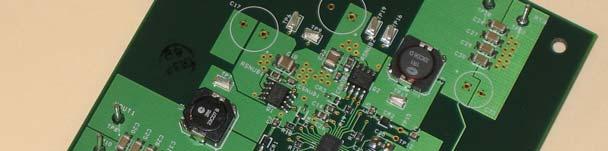
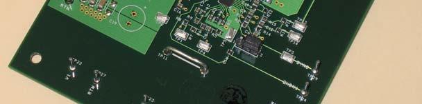
9 Silkscreen and Test Setup External Load + - VOUT2 INTEGRATED PRODUCTS LX1752 EVALUATION BOARD LXE1752 EVAL TP18 C24 C27 TP20 C21 TP19 TP16 C29 C30 + External Load - VOUT1 TP8 TP10 C20 C25 C17 L1 C28 C31 TP7 C19 TP6 + RSNUB1 + C18 TP9 Q1 C7 TP2 C22 + CR3 CSNUB1 C14 CR1 CR4 C16 R9 R8 TP11 C26 U1 C4 C3 TP1 CSNUB2 To second LX1752 SYNC pin, or external sync source TP22 TP27 TP23 TP26 TP21 TP25 V1 V2 VIN R18 R11 R7 RSNUB2 R19 R4 C2 R6 C5 C15 R17 R5 TP4 Q2 C11 C10 C9 R1 R2 C8 TP5 TP17 CR2 C13 1 R10 TP15 C6 R12 L2 C1 TP12 + R15 C12 R14 JB1 3 R16 R13 TP13 TP14 C23 TP3 SYNC TP29 SHDN1 TP24 SHDN2 TP28 This jumper (located on PCB bottom side) may be removed, allowing separate input power supply for each output + - Power Supply Figure 1. LX1752 Evaluation Board Test Setup Page 9
10 9 LX1752 Schematic +5VA JB1 R K 2 R1 1K R2 1K 3 C5 R7 R8 680pF 1.2K 20 C2 0.22uF R5 R6 TP1 TP2 4.87K 18.2K +5VA C6 V1 SYNC SHDN2 VIA TP5 C9 TP3 0.22uF C8 470pF TP4 28 VREF 27 PSET RFREQ SSEN1 GND SYNC SHDN2 U1 SSEN2 24 EA1-23 EO1 C4 C3 3.3nF SHDN1 CS1 VS1 VC1 NO STUFF R9 15K SHDN R K C7 0.1uF R10 1K 0.1uF TP6 2 Q1A FDS6910 TP TP C18 + C17 10uF NO STUFF 25V L1 2.5uH + C19 Rsnub1 NO STUFF 2.2 1/4W C31 C28 10uF NO STUFF 10V C25 10uF 10V VOUT1 C20 TP8 10uF 5 AMPS MAX 10V C10 NO STUFF 5 6 EA2- EO2 LX1752 HO1 HR R18 Q1B FDS Csnub1 680pF TP10 C11 3.3nF Vin 7 VIN THERMAL PAD CONNECTS TO SIGNAL GROUND LO TP11 R14 R12 C12 11K 470pF R13 1.6K C13 1uF 8 CS2 VS2 10 VC2 11 HO2 12 HR2 13 VCCL 14 LO2 15 PGND +5VA CR4 NO STUFF CR1 +5VA 20 AWG BUSS WIRE LOOP FOR SCOPE GROUND CONNECTION 24.9K TP13 R K R16 20 TP14 +5VA TP15 TP12 CR3 NO STUFF R K R19 0 C14 1.0uF C26 4.7uF 6.3V CMDSH-3 CR2 CMDSH-3 C15 C1 0.1uF 0.1uF C16 0.1uF TP16 4 Q2B FDS6910 V2 + C21 NO STUFF 6 5 TP17 L2 1.1uH 3 C22 10uF 25V VOUT2 TP19 2 Q2A FDS Rsnub /4W Csnub2 680pF + C23 NO STUFF C24 10uF 10V C24 10uF 10V C24 10uF 10V C24 TP18 10uF 5 AMPS MAX 10V TP20 TP21 TP22 TP23 TP24 Vin Vin V1 V1 V2 V2 SHDN1 SHDN1 VIN = 9V TO 15V AT TP21 TP25 20 AWG JUMPER WIRE TP26 TP27 SHDN2 SYNC TP28 SHDN2 SYNC TP29 Figure 2. LX1752 Evaluation Board Schematic Page 10
11 Printed Circuit Board Layout Recommendations Careful attention to PCB layout is necessary to insure proper operation with minimal noise generation. When laying out the PCB, these guidelines should be followed: 1) Keep the input capacitor, output capacitor, output inductor and output MOSFETs (upper and lower), close together, and tie all high current output returns directly to a suitable power ground plane. 2) Keep the high current ground return paths separate from the signal return paths. It is recommended that a separate signal ground plane be used, with a common tie point between the power ground plane and the signal ground plane established at the IC signal ground pin. 3) Place the input decoupling capacitor as close to the upper and lower MOSFETs as practical. Connections between this capacitor and the Upper and Lower MOSFETs Drain and Source connections, respectively, should be as short as practical. The LDO filter capacitor should be placed as close to the VCCL pin as practical. 4) PGND connection to the Source pin of the Lower MOSFET should be as short as practical, and should be established with a direct connection (using no vias) if possible. 5) VS X Pin connections should be Kelvin connected directly at the Upper MOSFET s drain pin(s). 6) HR X connection to the Upper MOSFET s Source pin should be as short as practical, and should be established with a direct connection (using no vias) if possible. 7) LOX and HOX should be connected to their respective MOSFET gate pins with as short a trace as practical, and should be established with a direct connection (using no vias) if possible. 8) The current sense (CS X ) resistor connection to the junction of the Upper MOSFET s Source, and the Lower MOSFET s drain should be as short as possible. 9) Place the CS X resistor as close to the CS X pin as possible. CSx pin is sensitive to capacitance to ground. If possible, minimize this capacitance by removing any ground plane area directly below the CSx pin pad and trace connection to the CSx resistor. 10) Place all compensation and feedback components as close to their respective error amplifier pins as practical. Keep the error amplifier input connections (EA X -) as short as possible. 11) Place the frequency programming resistor, R FREQ as close to the RFREQ and GND pins as practical. 12) For best thermal performance, the LX1752 thermal pad should be tied to signal ground, using 12 mil diameter (drill size) vias. Vias should be spaced 47mils apart in a grid array. See Figure 3 for details. Thermal vias are optional; the LX1752 will operate with reduced thermal performance without them. 4.56mm [0.180] 2.40mm [0.094] 5.56mm [0.219] 0.50mm [0.020] TYP. 24 PLS. 1.20mm [0.047] 3 PLS. 1.20mm [0.047] 4 PLS. Ø0.30mm [Ø0.012] OPTIONAL 6 PLS. 3.40mm [0.134] 0.30mm [0.012] MAX. 28 PLS. 0.25mm [0.010] TYP. 4 PLS. 0.81mm [0.032] Figure 3. 4x5mm LQ package suggested PCB pad layout. Page 11
: 3.5 in. X 4.0 in. (88.9mm x 101.")
12 LX1752 Evaluation Board Printed Circuit Layout PCB LAYOUT GUIDE TOP LAYER External PCB dimensions (W x H): 3.5 in. X 4.0 in. (88.9mm x 101.6mm) Page 12

13 PCB LAYOUT GUIDE INNER LAYER 1 POWER & SIGNAL GROUND PLANE Page 13

14 PCB LAYOUT GUIDE INNER LAYER 2 V1 & V2 POWER Page 14
15 PCB LAYOUT GUIDE BOTTOM LAYER (TOP SIDE VIEW MIRROR IMAGE FROM BOTTOM SIDE) Page 15
16 PCB LAYOUT GUIDE TOP SILKSCREEN & SOLDER MASK Page 16
17 Test Hookup and Operation The following is a demonstration scenario that can be used to evaluate the LX1752: 1) Connect a Power supply capable of 9V 15V, 5 Amps output, to VIN and (TP21 (+) and TP25 (-), respectively). Insure the supply is shut off before connecting. 2) Using an Oscilloscope, monitor test points TP7, TP17, and TP3. TP7 and TP17 are VOUT1 and VOUT2 switch nodes, respectively; TP3 is the LX1752 s sync signal. Trigger on the falling edge of the signal on TP3. Probe grounds may be connected to TP11. 3) Monitor VOUT1 (TP8 (+), and TP10 (-)), and VOUT2 (TP18 (+) and TP20 (-)) with a DMM. 4) Insure the position of the jumper JB1 is as follows: a. JB1 = jumper in position ) Power on the supply, and insure current is less than 100mA. Switch node waveforms on TP7 and TP17 should be continuous pulse waveforms with peak voltage levels approximately equal to the supply voltage. 6) SYNC signal present on TP3 should be a narrow, negative-going spike, approximately 5 Volts in amplitude. Frequency will be 800kHz +/- 5% 7) VOUT1 should measure 3.3 Volts, +/- 3%; VOUT2 should measure 1.2 Volts, +/- 3%. 8) Connect suitable loads to VOUT1 and VOUT2: TP8 (+) and TP10 (-) for VOUT1; TP18 (+) and TP20 (-) for VOUT2. Loads may be resistive or electronic loads. Loads should be able to handle at least 20 Watts (VOUT1), and 10 Watts (VOUT2). If using a resistive load, 0.66 Ohms 20 Watts (or higher) on VOUT1, and 0.24 Ohms 10 Watts (or higher) on VOUT 2 will load the outputs to their full rated capacity (assumes standard configuration with 3.3V and 1.2V output on VOUT1 and VOUT2, respectively). 9) Check short circuit limit: momentarily short VOUT1 with a small, heavy gauge wire. Average input power supply current will reduce significantly, and will cycle up/down in magnitude. Verify VOUT1 switch node signal at TP7 changes from a continuous pulse stream to a pulse stream that cycles on/off, with the on period approximately 4% of the overall on/off cycle. The on time for VOUT1 will be approximately 9.5 ms with the installed 0.22uF capacitor (C2). Verify that VOUT2 is unaffected and is still regulating. Remove the short across VOUT1 10) Momentarily short VOUT2 with a small, heavy gauge wire. Average input power supply current will reduce significantly, and will cycle up/down in magnitude. Verify VOUT2 switch node signal at TP17 changes from a continuous pulse stream to a pulse stream that cycles on/off, with the on period approximately 4% of the overall on/off cycle. The on time for VOUT2 will be approximately 9.5ms with the installed 0.22uF capacitor (C9). Verify that VOUT1 is unaffected and is still regulating. Remove the short across VOUT2 11) For 4 output interleaving, synchronize two LX1752 Evaluation Boards by connecting a wire between both evaluation board s SYNC signal test points (TP29). Place jumper JB1 on one of the evaluation boards in position 2-3, and leave jumper JB1 on the other board open. Monitoring test points TP7 and TP17 on both boards, verify that the switch node outputs are interleaved at approximate 90 intervals. Page 17
USER GUIDE FOR IR3899 EVALUATION BOARD
 IRDC3899-PV2 SupIRBuck TM DESCRIPTION USER GUIDE FOR IR3899 EVALUATION BOARD.2Vout The IR3899 is a synchronous buck converter, providing a compact, high performance and flexible solution in a small 4mm
USER GUIDE FOR IR3899 EVALUATION BOARD
 IRDC3899-PV8 SupIRBuck TM DESCRIPTION USER GUIDE FOR IR3899 EVALUATION BOARD.8Vout The IR3899 is a synchronous buck converter, providing a compact, high performance and flexible solution in a small 4mm
SupIRBuck TM IRDC3891 USER GUIDE FOR IRDC3891 EVALUATION BOARD DESCRIPTION BOARD FEATURES
 IRDC389 SupIRBuck TM USER GUIDE FOR IRDC389 EVUATION BOARD DESCRIPTION The IR389 is a dual synchronous buck converter, providing a compact, high performance and flexible solution in a small 5mm X 6mm Power
USER GUIDE FOR IRDC3823 EVALUATION BOARD
 IRDC3823-PV2 SupIRBuck TM DESCRIPTION USER GUIDE FOR IRDC3823 EVALUATION BOARD.2Vout The IR3823 is a synchronous buck converter, providing a compact, high performance and flexible solution in a small 3.5mm
SupIRBuck TM IRDC3840A USER GUIDE FOR IR3840A EVALUATION BOARD DESCRIPTION BOARD FEATURES
 SupIRBuck TM DESCRIPTION USER GUIDE FOR IR3840A EVALUATION BOARD The IR3840A is a synchronous buck converter, providing a compact, high performance and flexible solution in a small 5mmx6mm Power QFN package.
IRDC3810. Rev /14/2008 1
 IRDC380 03/4/2008 SupIRBuck TM DESCRIPTION USER GUIDE FOR IR380 EVALUATION BOARD IRDC380 The IR380 is a synchronous buck converter, providing a compact, high performance and flexible solution in a small
Obsolete. LX1800 SMBus TO ANALOG INTERFACE
 LX1800 SMBus TO ANALOG INTERFACE TM Page 1 INTRODUCING TO PRODUCT The LX1800 Evaluation Board is available from for evaluating the functionality and performance of the LX1800 SMBus to Analog Interface
LX7309EVB V to 48V Boost 15W Evaluation Board LX7309EVB-201 EVALUATION BOARD USER GUIDE. Page 1
 LX7309EVB-20 LX7309EVB - 20 2V to 48V Boost 5W Evaluation Board Copyright 203 Rev..2, 203-05-06 Page LX7309EVB-20 CONTENTS INTRODUCTION TO PRODUCT... 3 FEATURES:... 3 INPUT AND OUTPUT CONNECTION POINTS...
+Denotes lead-free and RoHS compliant.
 19-2446; Rev 1; 6/08 MAX17062 Evaluation Kit General Description The MAX17062 evaluation kit (EV kit) is a fully assembled and tested surface-mount PCB that provides the voltages required for active-matrix,
EV0055. Monolithic Power Systems. MP1530: Triple Output TFT Bias Converter. General Description. Absolute Maximum Ratings
 General Description The Evaluation Board is designed to demonstrate the capabilities of MPS MP50 triple output step-up converter which is capable of powering a TFT panel from a regulated.v or 5V. The MP50
Single Phase Synchronous Buck Converter using ip1001 Overview
 REFERENCE DESIGN IRDCiP11-B, 2kHz to 3kHz, 2A, 5V IN to 12V IN Single Phase Synchronous Buck Converter using ip11 Overview In this document, Table 1 and Figure 1 are provided to enable engineers to easily
HX4002 HX1001. White LED Backlighting Li-Ion Battery Backup Supplies Local 3V to 5V Conversion Smart Card Readers PCMCIA Local 5V Supplies
 HX1001 Low Noise, Regulated Charge Pump DC/DC Converter Features Fixed 5V±4% Output VIN Range: 2.7V ~ 5V Output Current: up to 250mA (V IN =4.5V) Low Noise Constant Frequency Operation Shutdown Current:
MAX5097A Evaluation Kit. Evaluates: MAX5097A
 19-0718; Rev 0; 1/07 MAX5097A Evaluation Kit General Description The MAX5097A evaluation kit (EV kit) demonstrates the MAX5097A in a standard application circuit demonstrating high efficiency. The EV kit
Maxim Integrated Products 1
 19-2881; Rev 0; 6/03 General Description The MAX1543 evaluation kit (EV kit) is a fully assembled and tested surface-mount circuit board that provides the voltages and features required for active-matrix,
XR76117/21. PowerBlox 15A and 20A Synchronous Step Down COT Regulator GENERAL DESCRIPTION EVALUATION BOARD MANUAL FEATURES
 XR76117/21 November 2016 GENERAL DESCRIPTION The XR76117 and XR76121 are synchronous step-down regulators combining the controller, drivers, bootstrap diode and MOSFETs in a single package for point-of-load
MAXREFDES108#: NON-ISOLATED 12V/1A POE POWERED DEVICE POWER SUPPLY
 System Board 6289 MAXREFDES108#: NON-ISOLATED 12V/1A POE POWERED DEVICE POWER SUPPLY To meet the increasing demands for non-isolated Power over Ethernet (PoE) power solutions, Maxim has developed innovative,
GENERAL DESCRIPTION EVALUATION BOARD MANUAL
 s June 2012 Rev. 1.1.1 GENERAL DESCRIPTION The XRP7714EVB-DEMO-1, XRP7714EVB- DEMO-2, and the XRP7714-DEMO-2P Demo boards are complete, working, four channel, power systems measuring either 2 x 2, or 2
BCT mA Buck/Boost Charge Pump LED Driver
 BCT3140 GENERAL DESCRIPTION The BCT3140 is a current-regulated charge pump ideal for powering high brightness LEDs for camera flash applications. The charge pump can be set to regulate two current levels
2 AA Cell to 3.3V USB On-The-Go Devices White LED Drivers Handheld Devices. The HM3200B is available in the 6-pin SOT23-6.
 Low Noise, Regulated Charge Pump DC/DC Converter Features Fixed 3.3V ± 4% Output VIN Range: 1.8V to 5V Output Current: 100mA Constant Frequency Operation at All Loads Low Noise Constant Frequency (1.2MHz)
Microsemi Power Management Solution for A2F-EVAL-KIT-2
 PM Solution Power Management Solution for A2F-EVAL-KIT-2 Author: Dennis Mattocks One Enterprise Aliso Viejo, CA 92656 USA (800) 713 4113, (949) 380 6100 Page 1 PM Solution Scope This document presents
General Description. Features. Component List. Component Suppliers
 General Description The MAX5911 evaluation kit (EV kit) is a fully assembled and tested surface-mount circuit board that demonstrates the MAX5911 fully integrated hot-swap solution for negative supply
BG2E Universal Gate Drive Prototype Board
 Application NOTES: First Release: March 23, 200 BG2E Universal Gate Drive Prototype Board Description: BG2E is a fully isolated two channel gate drive circuit designed for use with dual NX-L series IGBT
Universal PMIC 40V Quad Output Digital PWM/PFM Demo Board
 December 2014 Rev. 1.0.0 GENERAL DESCRIPTION The XR77129EVB-DEMO-1 board is a complete four channel power system. It is configured to provide 5.0V, 12V, 3.3V and 2.5V at a maximum of 5A, 3A, 5A and 10A
DIO5151B 700mA/1A Buck/Boost Charge Pump LED Driver
 Rev 0.1 Features Output Current : DIO5151BED8: 700mA DIO5151BCD10: 1A Up to 90% Efficiency in Torch Mode Adjustable FLASH Mode Current 1 and 2 Automatic Modes for High Efficiency Input Voltage Range: 3V
Maxim Integrated Products 1
 9-366; Rev ; 2/06 General Description The MAX8727 evaluation kit (EV kit) is a fully assembled and tested surface-mount circuit board that contains a pulse-width-modulated (PWM) step-up DC-DC converter.
2. Control Pin Functions and Applications
 IMARY CONTROL ( PIN) Module Enable / Disable. The module can be disabled by pulling the below 2.3 V with respect to the Input. This should be done with an open-collector transistor, relay, or optocoupler.
ISL91117II7-EVZ, ISL91117IIA-EVZ Evaluation Boards
 Sameer Dash ISL91117II7-EVZ, ISL91117IIA-EVZ Evaluation Boards Description The ISL91117 is a highly-integrated boost switching regulator for battery powered applications. The device provides a power supply
Universal PMIC Quad Output Digital PWM/PFM Demo Board
 December 2014 Rev. 1.0.0. GENERAL DESCRIPTION The XR77128EVB-DEMO-1 board is a complete four channel power system. It is configured to provide 3.3V, 2.5V, 1.5V and 1V at a maximum of 3A, 3A, 5A and 10A
Full-chip PRM -RS Customer Board User Guide
 USER GUIDE UG:009 For use with PCB part number: 35306 Full-chip PRM -RS Customer Board User Guide Contents Page Introduction 1 Features 2 General 2 4 Schematic 5 Bill of Material 7 VTM Customer Boards
IRDCiP1201-A, 300kHz, Dual 15A, 3.14V IN
 REFERENCE DESIGN International Rectifier 33 Kansas Street, El Segundo, CA 95 USA IRDCiP11-A IRDCiP11-A, 3kHz, Dual 15A, 3.V IN to 5.5V IN Dual Output Synchronous Buck Converter using ip11 Overview The
BG2D Solderless Connection Gate Drive Prototype Board
 Application NOTES: First Release: May, 2008 BG2D Solderless Connection Gate Drive Prototype Board Description: The BG2D is a two channel gate drive circuit for that the dual NX series modules pins plug
Figure 1: AAT1106 Evaluation Board.
 Introduction The AAT1106 Evaluation Board contains a fully tested 600mA, 1.5MHz Step-Down DC/DC Regulator. The circuit has an input voltage range of 2.5V to 5.5V and four preset selectable outputs (1.2V,
Obsolete LX1811 EVALUATION KIT USER S GUIDE LX1811 EVALUATION BOARD USER GUIDE
 LX1811 EVALUATION KIT USER S GUIDE INTEGRATED PRODUCTS Page 1 LX1811 Evaluation Board Description The LX1811 evaluation board implements a typical design using the LX1811 TEC controller driver and is intended
QUICK START GUIDE FOR DEMONSTRATION CIRCUIT 1142A-A/B USB POWER MANAGER WITH Li-ION CHARGER AND THREE STEP-DOWN REGULATORS
 DESCRIPTION The DC1142A-A/B contains the LTC3557/LTC3557-1 Power Management Integrated Circuit (PMIC) plus the LT3480EDD high voltage buck controller. The LTC3557/LTC3557-1 is a highly integrated power
QUICK START GUIDE FOR DEMONSTRATION CIRCUIT 740 TRACKER/SEQUENCER DEMO BOARD
 DESCRIPTION QUICK START GUIDE FOR DEMONSTRATION CIRCUIT 740 LTC2922 Demonstration circuit 740 is a tracker/sequencer demo board featuring the LTC2922 that monitors up to five external power supplies and
PI33xx-xx-EVAL1 Cool-Power ZVS Buck Regulator Evaluation Board
 USER GUIDE UG:302 PI33xx-xx-EVAL1 Cool-Power ZVS Buck Regulator Evaluation Board Contents Page Introduction 1 Evaluation Board Supply & Load Connections 2 Bill of Materials 3 Evaluation Board Notes Optional
MAX17105 Evaluation Kit/Evaluation System
 19-4589; Rev 0; 4/09 MAX17105 Evaluation Kit/Evaluation System General Description The MAX17105 evaluation system (EV system) consists of the MAX17105 evaluation kit (EV kit) and the Maxim CMAXQUSB+ command
EVAL-INAMP-62RZ/82RZ/82RMZ
 Evaluation Boards for the AD620 Series and and the AD8220 Series Instrumentation Amplifiers EVAL-INAMP-62RZ/82RZ/82RMZ FEATURES 3 generic, easy-to-use PC boards Support several related in-amp products
EV1531DQ-002A Low Power, Triple Output Step-Up Plus Charge Pump for TFT Bias
 Monolithic Power Systems EV1531DQ-002A Low Power, Triple Output Step-Up Plus Charge Pump for TFT Bias GENERAL DESCRIPTION The EV1531DQ-002A Evaluation Board is designed to demonstrate the capabilities
MIC24051 Evaluation Board
 6A, High-Efficiency, Synchronous DC/DC Buck Regulator with Hyper Speed Control SuperSwitcher II General Description The MIC2451 DC/DC synchronous buck regulator operates over an input supply range of 4.5V
S IEEE 802.3af/at-Compliant PSE Circuit. Maxim Integrated Products 1
 19-5740; Rev 0; 1/11 MAX5971A Evaluation Kit General Description The MAX5971A evaluation kit (EV kit) is a fully assembled and tested surface-mount circuit board featuring an Ethernet single-port power-sourcing
Si9143 High-Performance Processor Controller Demo Board
 Si9143 High-Performance Processor Controller Demo Board Voltage Mode Control Synchronous Buck Converter Short Circuit Current Limiting Over-Voltage Protection Output Current to 15 A Power Good Signal +5
MAX17116Q Evaluation Kit Evaluates: MAX17116 in a 24-Pin TQFN Package
 19-5846; Rev 0; 5/11 MAX17116Q Evaluation Kit General Description The MAX17116Q evaluation kit (EV kit) is a fully assembled and tested surface-mount PCB that evaluates the MAX17116 dual-output DC/DC power
+Denotes lead-free and RoHS compliant. C38 C43, C62, C64, C65, C66, C68, C70, C72, C73, C74, C76 C44 C49, C67, C75 C63, C69, C71, C77
 19-4354; Rev 0; 10/08 MAX17108 Evaluation Kit General Description The MAX17108 evaluation kit (EV kit) is a fully assembled and tested surface-mount PCB that evaluates the MAX17108 10-channel, high-voltage
MAX16128/MAX16129 Evaluation Kits. Evaluate: MAX16128/MAX General Description. Features. Component List
 General Description The MAX16128/MAX16129 evaluation kits (EV kits) demonstrate high overvoltage protection of the MAX16128/ MAX16129 for automotive applications that must survive load-dump and high-voltage
Achieving EMV Electrical Compliance with the Teridian 73S8024RN
 August 2005 Achieving EMV Electrical Compliance with the Teridian 1 Introduction This application note highlights particular testing considerations required to achieve compliance for payment systems smart
APPLICATION NOTES. Wire Gauge and Distance to Load
 The RB, RW and RM series of power supplies were designed as military grade, stand alone devices requiring no external components for operation. The entire series are 60 to 200 khz, fixed frequency, switching
Designer s Guide to the ISL95813 Evaluation Board
 Designer s Guide to the ISL95813 Evaluation Board Description The ISL95813 single-phase controller provides a fully compliant VR12.6 power supply solution for Intel microprocessors. It provides a tightly
BG1B Universal Gate Drive Prototype Board
 BG1B Universal Gate Drive Prototype Board Description: The BG1B is a single channel gate drive circuit board for high power IGBT modules. The BG1B utilizes Powerex hybrid gate drivers and DC-to-DC converters
/ Vref) 1]. Set R7=R14=1k,Vref=0.8V 2. V OUT2
![/ Vref) 1]. Set R7=R14=1k,Vref=0.8V 2. V OUT2](/thumbs/82/85326025.jpg "/ Vref) 1]. Set R7=R14=1k,Vref=0.8V 2. V OUT2") REFERENCE DESIGN International Rectifier 233 Kansas Street, El Segundo, CA 9245 USA IRDCiP122-A, 3kHz, Dual 15A, 5.5V IN to 13.2V IN Dual Output Synchronous Buck Converter using ip122 Overview The ip122
REFERENCE DESIGN International Rectifier 233 Kansas Street, El Segundo, CA 9245 USA IRDCiP122-A, 3kHz, Dual 15A, 5.5V IN to 13.2V IN Dual Output Synchronous Buck Converter using ip122 Overview The ip122
GENERAL DESCRIPTION FEATURES EVALUATION BOARD
 XRP773EVB-DEMO- April 20 Rev..0.0 GENERAL DESCRIPTION The XRP773EVB-DEMO- Demo board is a complete, working, 3 channel, power system measuring.75 x.75 capable of producing over 30 watts. It is optimized
UG-108 Rev 1.0, 14-Oct-2018
 ACT4921EVK1-301 User s Guide Description This document describes the characteristic and operation of the Active Semi ACT4921EVK1-301 evaluation kit (EVK). It provides setup and operation instructions,
GENERAL DESCRIPTION APPLICATIONS FEATURES TYPICAL APPLICATION DIAGRAM
 August 2009 Rev. 2.0.0 GENERAL DESCRIPTION The SP6686 is a current-regulated charge pump ideal for powering high brightness LEDs for camera flash applications. The charge pump can be set to regulate two
HFRD REFERENCE DESIGN High-Frequency XFP Host Board. Reference Design: (Includes Integrated RS-232 to I 2 C Conversion)
") Reference Design: HFRD-18.0 Rev. 7; 11/09 REFERENCE DESIGN High-Frequency XFP Host Board (Includes Integrated RS-232 to I 2 C Conversion) Reference Design: High-Frequency XFP Host Board Table of Contents
Reference Design: HFRD-18.0 Rev. 7; 11/09 REFERENCE DESIGN High-Frequency XFP Host Board (Includes Integrated RS-232 to I 2 C Conversion) Reference Design: High-Frequency XFP Host Board Table of Contents
Application Suggestions for X2Y Technology
 Application Suggestions for X2Y Technology The following slides show applications that would benefit from balanced, low inductance X2Y devices. X2Y devices can offer a significant performance improvement
2:1 Input Voltage Range 2.25kVDC Isolation UL Certified Efficiency up to 88% Ultraminiature Open Frame SMD No Minimum Load Required
 Features Regulated Converters Description 2:1 Input Voltage Range 2.25kV Isolation UL Certified Efficiency up to 88% Ultraminiature Open Frame SMD No Minimum Load Required The RP15-SOF series, are SMD
LLIA90 LED ARRAY 90 LED Array Illuminator. LLIA90 LED Illuminator Array
 LLIA90 LED Illuminator Array The LLIA90 is a high-quality and high-performance multi-purpose LED illuminator array. It has a built-in regulator and a photocell control circuit for automatic LED array on/off
EV161-S-00A Power Solution with Ultra Low Standby Power, Integrates Switching Regulator, Linear Regulator and Relay Driver
 The Future of Analog IC Technology EV6-S-00A Power Solution with Ultra Low Standby Power, Integrates Switching Regulator, Linear Regulator and Relay Driver DESCRIPTION The EV6-S-00A Evaluation Board is
ISL91108IIA-EVZ/ISL91108IIN-EVZ Evaluation Board User Guide
 Author: Sameer Dash ISL91108IIA-EVZ/ISL91108IIN-EVZ Evaluation Board User Guide Evaluation Board Features ISL91108 high efficiency buck-boost regulator Input voltage rating from 1.8V to 5.5V Resistor programmable
LDD M SERIES INSTRUCTION MANUAL LDD M SERIES
 TM LDD M SERIES LDD M SERIES INSTRUCTION MANUAL P O Box Bozeman, MT 9 Phone (0) -90 Fax (0) -9 email sales@wavelengthelectronics.com www.wavelengthelectronics.com TABLE OF CONTENTS Features... Customer
MIC A Evaluation Board
 75V/4A Hyper Speed Control Synchronous DC/DC Buck Regulator General Description meter and V IN at Vin and GND terminals with voltmeter. Do not apply power until Step 5. The MIC28500 DC/DC regulator operates
Features. General Description. Component List
 MAX5988A Evaluation Kit Evaluates: MAX5988A General Description The MAX5988A evaluation kit (EV kit) is a fully assembled and tested surface-mount circuit board featuring an Ethernet port, network powered-device
PAM8304-EV board User Guide AE Department. Date Revision Description Comment
 1. Revision Information -EV board User Guide AE Department Date Revision Description Comment 2013/5/31 V1.0 Initial release 1 of 5 2. Key Features Supply Voltage from 2.8V to 6.0V 3.0W@10% THD Output with
YB1300S Switched Capacitor Boost Converter 5V/4.5V
 Description The YB1300S is a switched capacitor DC/DC boost converter that produces a regulated 5V output. The input voltage range is from 2.7V to 5.0V that makes the YB1300S ideally for a single cell
Test Methods for DC/DC Power Modules
 Test Methods for DC/DC Power Modules Design Note 027 Flex Power Modules Precautions Abstract A user may have the desire to verify or characterize the performance of DC/DC power modules outside the system
73S8014R/RN/RT 20SO Demo Board User Manual July, 2008 Rev. 1.0 UM_8014_010
 Simplifying System Integration TM 73S804R/RN/RT 0SO Demo Board User Manual July, 008 Rev..0 UM_804_00 73S804R/RN/RT 0SO Demo Board User Manual UM_804_00 008 Teridian Semiconductor Corporation. All rights
EV-110 AAT1157 EVAL 1MHz 1.4A Buck Regulator
 Introduction The AAT1157 evaluation board demonstrates performance, along with the suggested size and placement of external components, for the AAT1157 integrated buck regulator. The external components
WS4601 WS4601. Descriptions. Features. Applications. Order information. 80mΩ, Current Limited, Power Distribution Switch
 80mΩ, Current Limited, Power Distribution Switch www.sh-willsemi.com Descriptions The is high-side switch with ultra-low ON resistance P-MOSFET. Integrated current-limit function can limit inrush current
IRDCiP1206-B. Overview. Demoboard Quick Start Guide Initial Settings:
 REFERENCE DESIGN IRDCiP1206-B International Rectifier 233 Kansas Street, El Segundo, CA 90245 USA IRDCiP1206-B: 300 khz, Dual Output, Synchronous Buck Converter using ip1206 Overview This reference design
PI5101-EVAL1 μr DS(on) FET TM Series
 FET TM Series") PI5101-EVAL1 3.3V/60A High Side Active ORing Evaluation Board User Guide PI5101-EVAL1 μr DS(on) FET TM Series Content Page μr DS (on)fet Series Introduction... 1 Product Description... 2 Schematic... 3
PI5101-EVAL1 3.3V/60A High Side Active ORing Evaluation Board User Guide PI5101-EVAL1 μr DS(on) FET TM Series Content Page μr DS (on)fet Series Introduction... 1 Product Description... 2 Schematic... 3
POL BMR465 Evaluation Board
 User Guide POL BMR465 Evaluation Board ROA 170 64 User Guide User Guide 2 Contents 1 Introduction... 3 1.1 Prerequisites... 3 2 Reference Board ROA 170 64... 4 3 USB-PMBus adapter... 5 3.1 Connection of
February 2003 PMP EVMs SLVU081
 User s Guide February 2003 PMP EVMs SLVU081 IMPORTANT NOTICE Texas Instruments Incorporated and its subsidiaries (TI) reserve the right to make corrections, modifications, enhancements, improvements, and
PI354X-00 Evaluation Board User Guide 36 V to 60 V IN, 2.5, 3.3, 5.0, and 12 V OUT Cool-Power Buck Regulator & LED Driver
 USER GUIDE UG: PIX- Evaluation Board User Guide V to V IN,.,.,., and V OUT Cool-Power Buck Regulator & LED Driver Contents Page Evaluation Board Supply & Load Connections PI--EVAL PI--EVAL PI--EVAL PI--EVAL
MP201 Dying Gasp Storage and Release Control IC
 The Future of Analog IC Technology MP201 Dying Gasp Storage and Release Control IC DESCRIPTION The MP201 is a dying gasp storage and release controller. It charges storage capacitor from the input during
PT SERIES SIP Package
 FEATURES Industry Standard SIP 8 Package 3 Watts Isolated Output 2:1 Input Range Regulated Outputs Up to 86 % Efficiency -40 C to +85 operating temperature range Remote On/Off logic control Continuous
POL BMR466 Evaluation Board
 1/28701- Rev A May 2018 POL BMR466 Evaluation Board 2 1/28701- Rev A May 2018 Contents 1 Introduction... 3 1.1 Prerequisites... 3 2 Reference Board... 4 3 USB to PMBus adaptor... 5 3.1 Connection of Flex
HM9708 HM9708. Battery-Powered Equipment Motherboard USB Power Switch USB Device Power Switch Hot-Plug Power Supplies Battery-Charger Circuits DC+ VIN
 200mΩ Power Distribution Switches Features 200mΩ Typ. High-Side MOSFET 0.8A Current Limit (V IN =3.0V) Wide Input Voltage Range: 2V ~ 5.5V Soft Start Thermal Protection Small SOT-23-5 Package Minimizes
FEATURES SPECIFICATION. Rev 2.0, Dedicated 5V/2.1A Power Bank Solution. Input voltage. Boost outpu. Boost output current limit 2.
 ACT2802 Demo Board Application Report Rev 2.0, 05-Aug-2014 Dedicated 5V/2.1A Power Bank Solution FEATURES 5V/3.0A input current limit 2.0A battery charge current 5V/2.1A boost output current 2.5A boost
Application Note. Mil-COTS. MCOTS-C-270-xx-HT DC/DC CONVERTER. 270Vin. Designed and Manufactured in the USA
 Application Note Mil-COTS MCOTS-C-270-xx-HT DC/DC CONVERTER 270Vin Designed and Manufactured in the USA This application note explains how to implement the features of a d converter. Features include active
UG-106 Rev 1.0, 16-November-2017
 ACT490EVK- User s Guide UG-06 Description This document describes the characteristic and operation of the Active Semi ACT490EVK- evaluation kit (EVK). It provides setup and operation instructions, schematic,
MAX14808 Evaluation System Evaluates: MAX14808
 General Description The MAX14808 evaluation kit (EV kit) provides a proven design to evaluate the MAX14808 high-voltage, highfrequency pulse driver IC. The MAX14808 evaluation system (EV system) consists
Propeller Project Board USB (#32810)
") Web Site: www.parallax.com Forums: forums.parallax.com Sales: sales@parallax.com Technical: support@parallax.com Office: (916) 624-8333 Fax: (916) 624-8003 Sales: (888) 512-1024 Tech Support: (888) 997-8267
Web Site: www.parallax.com Forums: forums.parallax.com Sales: sales@parallax.com Technical: support@parallax.com Office: (916) 624-8333 Fax: (916) 624-8003 Sales: (888) 512-1024 Tech Support: (888) 997-8267
S +10.8V to +13.2V Supply Voltage S Output Voltages
 19-5088; Rev 0; 12/09 General Description The MAX17113 evaluation kit (EV kit) is a fully assembled and tested surface-mount PCB that provides the voltages and features required for thin-film transistor
AN-719 APPLICATION NOTE One Technology Way P.O. Box 9106 Norwood, MA Tel: 781/ Fax: 781/
 APPLICATION NOTE One Technology Way P.O. Box 9106 Norwood, MA 02062-9106 Tel: 781/329-4700 Fax: 781/326-8703 www.analog.com ADuC7024 Evaluation Board Reference Guide MicroConverter ADuC7024 Development
400mA Buck/Boost Charge Pump LED Driver
 4mA Buck/Boost Charge Pump LED Driver SP6686 FEATURES Output Current up to 4mA Up to 94% Efficiency in Torch Mode Automatic Softstart Limits Inrush Current Adjustable FLASH Mode x1 and x2 Automatic Modes
QUICK START GUIDE FOR DEMONSTRATION CIRCUIT 995A ADJUSTABLE LDO LINEAR REGULATOR LT3080EDD DESCRIPTION
 LT3080EDD DESCRIPTION Demonstration circuit 995A is an adjustable 1.1A linear regulator featuring LT 3080. Architected as a precision current source and voltage follower, it allows this new regulator to
CLK1, CLKIN, CLKOUT, OUTA, OUTB
 9-82; Rev 2; 5/ Evaluation Kit General Description The evaluation kit (EV kit) is a fully assembled and tested circuit board that contains all the components necessary for evaluating the. The is a dual,0-bit,
20W DC-DC Converter P20J-Series
 20W - Converter P20J-Series Wide 4:1 input range Efficiency up to 89 % Adjustable output voltage Remote control on / off 3000 V isolation Continuous short circuit protection Over voltage protection MTBF
MAX17061 Evaluation Kit/Evaluation System
 19-4070; Rev 1; 10/08 MAX17061 Evaluation Kit/Evaluation System General Description The MAX17061 evaluation system (EV system) consists of the MAX17061 evaluation kit (EV kit) and the Maxim CMAXQUSB+ command
UG110 Rev 1.0, 07-Jun-2018
 Description ACT2861EVK1-201 Rev B User s Guide UG110 This document describes the characteristic and operation of the Active Semi ACT2861EVK1-201 evaluation kit (EVK). It provides setup and operation instructions,
Technical Note. Design Considerations when using NOR Flash on PCBs. Introduction and Definitions
 Technical Note Design Considerations when using NOR Flash on PCBs Introduction and Definitions TN-13-30: NOR Flash Memory: PCB Design Considerations Introduction and Definitions Table 1: Definitions Term
S12VR Hardware Design. Guidelines. 1 Introduction. 2 Hardware Design. Guidelines. 2.1 Voltage regulator. Freescale Semiconductor
 Freescale Semiconductor Document Number: AN4643 Application Note Rev 1, 10/2013 S12VR Hardware Design Guidelines by: Carlos Aceff 1 Introduction This document lists the required external components and
DEI5090 SINGLE-RAIL ARINC 429 LINE DRIVER
 Device Engineering Incorporated 385 East Alamo Drive Chandler, AZ 85225 Phone: (480) 303-0822 Fax: (480) 303-0824 E-mail: admin@deiaz.com DEI5090 SINGLE-RAIL ARINC 429 LINE DRIER FEATURES Operates from
The primary side feedback single-stage
 The primary side feedback single-stage active PFC constant current LED driver D8063-18-30W Panel light Application Note May, 3 rd. 2016 Feature Single-stage active high power factor correction, high PF
MIC5281. Features. General Description. Applications. Typical Application. 120V IN, 25mA, Ultra-Low IQ, High-PSRR Linear Regulator
 120V IN, 25mA, Ultra-Low IQ, High-PSRR Linear Regulator General Description The high-performance linear regulator offers a very-wide input operating voltage range, up to 120V DC, and supplies an output
MP5455 Power Back-Up Manager
 MP5455 Power Back-Up Manager The Future of Analog IC Technology DESCRIPTION The MP5455 is designed to provide back-up power in the event of a power failure. The internal input current limit block with
Pololu 12V Step-Up/Step-Down Voltage Regulator S10V2F12
 Pololu 12V Step-Up/Step-Down Voltage Regulator S10V2F12 Overview The Pololu step-up/step-down voltage regulator S10V2F12 is a switching regulator (also called a switched-mode power supply (SMPS) or DC-to-DC
Reference Design. 50-W Push-Pull Converter Reference Design Using the UCC38085 (PR100B) Reference Design
 Reference Design") Reference Design 50-W Push-Pull Converter Reference Design Using the UCC38085 (PR100B) Reference Design 1 50-W Push-Pull Converter Reference Design Using the UCC38085 (PR100B) John Bottrill System Power
Reference Design 50-W Push-Pull Converter Reference Design Using the UCC38085 (PR100B) Reference Design 1 50-W Push-Pull Converter Reference Design Using the UCC38085 (PR100B) John Bottrill System Power
DEMO MANUAL DC2016A LTM V IN, 5.4A Buck-Boost μmodule Regulator. Description
 Description Demonstration circuit 216A features the LTM854, a synchronous buck-boost μmodule regulator that accepts input voltages lower, higher or the same as the output, but is also highly efficient
XRD87L85 Low-Voltage CMOS 8-Bit High-Speed Analog-to-Digital Converter
 Low-Voltage CMOS 8-Bit High-Speed Analog-to-Digital Converter April 2002-1 FEATURES 8-Bit Resolution Up to 10 MHz Sampling Rate Internal S/H Function Single Supply: 3.3V VIN DC Range: 0V to V DD VREF DC