NHD C0220BiZ FS(RGB) FBW 3VM
|
|
|
- Basil Evans
- 5 years ago
- Views:
Transcription
 B 6:00 view W Wide Temp ( 20 C ~ +70 C) 3V 3.3V power supply M with Mounting holes RoHS Compliant Newhaven Display International, Inc.")
1 NHD C0220BiZ FS(RGB) FBW 3VM COG (Chip On Glass) Character Liquid Crystal Display Module NHD Newhaven Display C0220 COG 2 lines x 20 characters BiZ Model, with I2C interface F Transflective S(RGB) Side LED backlights Red, Green, and Blue F FSTN (+) B 6:00 view W Wide Temp ( 20 C ~ +70 C) 3V 3.3V power supply M with Mounting holes RoHS Compliant Newhaven Display International, Inc Technology Drive, Suite 101 Elgin IL, Ph: Fax: nhtech@newhavendisplay.com nhsales@newhavendisplay.com
2 Document Revision History Revision Date Description Changed by 0 7/8/2009 Initial Release CL 1 7/10/2009 Mechanical Drawing updated BE 2 9/8/2009 Backlight supply current BE 3 10/9/2009 Updated Electrical Characteristics MC 4 12/9/2009 Updated Backlight Power supply and Current MC Functions and Features 2 lines x 20 characters Built in ST7036i controller with I2C interface 3.3V power supply 1/16 duty, 1/5 bias Built in DC supply for VLCD (requires 2 external capacitors)
3
4 RK GK BK NHD-C0220BiZ-FSRGB-FBW-3VM Newhaven Display 7/10/09
5 Pin Description and Wiring Diagram Pin No. Symbol External Function Description Connection 1 RST MPU Active LOW Reset 2 SCL MPU Serial Clock (requires pull up resistor) 3 SDA MPU Serial Data (requires pull up resistor) 4 VSS Power Supply GND 5 VDD Power Supply +3.3V 6 VOUT CAP Voltage booster circuit connect to 1uF cap to VSS or VDD 7 C1+ CAP Connect to 1uF cap to PIN8 8 C1 CAP Connect to 1uF cap to PIN7 Recommended LCD connector: 2.0mm pitch pins, solder directly into PCB Backlight connector: 3.0mm pitch pins, solder directly into PCB Mates with: Capacitance 0.47uF~2.2uF Recommended value = 1uF
6 Electrical Characteristics Item Symbol Condition Min. Typ. Max. Unit Operating Temperature Range Top Absolute Max ⁰C Storage Temperature Range Tst Absolute Max ⁰C Supply Voltage VDD V Supply Current IDD VDD=3.3V 1 ma Supply for LCD (contrast) VDD V0 VLCD=VDD V V H Level input Vih 0.7VDD VDD V L Level input Vil V H Level output Voh 0.7VDD VDD V L Level output Vol 0.8 V Backlight Supply Voltage RED VLED 2.2 V Backlight Supply Current RED Iled 10 ma Backlight Supply Voltage GREEN VLED 3.3 V Backlight Supply Current GREEN Iled 10 ma Backlight Supply Voltage BLUE VLED 3.3 V Backlight Supply Current BLUE Iled 12 ma Optical Characteristics Item Symbol Condition Min. Typ. Max. Unit Viewing Angle Vertical AV Cr ⁰ Viewing Angle Horizontal AH Cr ⁰ Contrast Ratio Cr 6 Response Time (rise) Tr ms Response Time (fall) Tf ms
7 Controller Information Built in ST7036i. Download specification at Slave Address = 0x78

8 Table of Commands
9

10 Built in Font Table (OPR1 = 0, OPR2 = 0)
11 Example Initialization Program /**************************************************** * Initialization For ST7036i * *****************************************************/ void init_lcd() { I2C_Start(); I2C_out(Slave);//Slave=0x78 I2C_out(Comsend);//Comsend = 0x00 I2C_out(0x38); delay(10); I2C_out(0x39); delay(10); I2C_out(0x14); I2C_out(0x78); I2C_out(0x5E); I2C_out(0x6D); I2C_out(0x0C); I2C_out(0x01); I2C_out(0x06); delay(10); I2C_Stop(); } /*****************************************************/ /**************************************************** * Output command or data via I2C * *****************************************************/ void I2C_out(unsigned char j) //I2C Output { int n; unsigned char d; d=j; for(n=0;n<8;n++){ if((d&0x80)==0x80) SDA=1; else SDA=0; d=(d<<1); SCL = 0; SCL = 1; SCL = 0; } SCL = 1; while(sda==1){ SCL=0; SCL=1; } SCL=0; } /*****************************************************/
12 /**************************************************** * I2C Start * *****************************************************/ void I2C_Start(void) { SCL=1; SDA=1; SDA=0; SCL=0; } /*****************************************************/ /**************************************************** * I2C Stop * *****************************************************/ void I2C_Stop(void) { SDA=0; SCL=0; SCL=1; SDA=1; } /*****************************************************/ /**************************************************** * Send string of ASCII data to LCD * *****************************************************/ void Show(unsigned char *text) { int n,d; d=0x00; I2C_Start(); I2C_out(Slave); //Slave=0x78 I2C_out(Datasend);//Datasend=0x40 for(n=0;n<20;n++){ I2C_out(*text); ++text; } I2C_Stop(); } /*****************************************************/ /*****************************************************/ /*****************************************************/
13 Quality Information Test Item Content of Test Test Condition Note High Temperature storage Endurance test applying the high +80⁰C, 200hrs 2 storage temperature for a long time. Low Temperature storage Endurance test applying the low storage 30⁰C, 200hrs 1,2 temperature for a long time. High Temperature Operation Endurance test applying the electric stress (voltage & current) and the high thermal stress for a long time. +70⁰C 200hrs 2 Low Temperature Operation High Temperature / Humidity Operation Thermal Shock resistance Vibration test Endurance test applying the electric stress (voltage & current) and the low thermal stress for a long time. Endurance test applying the electric stress (voltage & current) and the high thermal with high humidity stress for a long time. Endurance test applying the electric stress (voltage & current) during a cycle of low and high thermal stress. Endurance test applying vibration to simulate transportation and use. Static electricity test Endurance test applying electric static discharge. Note 1: No condensation to be observed. Note 2: Conducted after 4 hours of storage at 25⁰C, 0%RH. Note 3: Test performed on product itself, not inside a container. Precautions for using LCDs/LCMs See Precautions at Warranty Information and Terms & Conditions 20⁰C, 200hrs 1,2 +60⁰C, 90% RH, 96hrs 1,2 20⁰C,30min > 25⁰C,5min > 70⁰C,30min = 1 cycle 10 cycles 10 55Hz, 15mm amplitude. 60 sec in each of 3 directions X,Y,Z For 15 minutes VS=800V, RS=1.5kΩ, CS=100pF One time 3

 Description The ST7036 dot-matrix liquid crystal display controller can display alphanumeric, Japanese kana characters, and symbols.")
14 ST Sitronix ST7036 Dot Matrix LCD Controller/Driver Features 5 x 8 dot matrix possible Low power operation support: to 5.5V Range of LCD driver power to 7.0V 4-bit, 8-bit, serial or I 2 C-bus MPU interface enabled 80 x 8-bit display RAM (80 characters max.) 10,240-bit character generator ROM for a total of 256 character fonts(max) 64 x 8-bit character generator RAM(max) Support two display mode: 16-com x 100-seg and 80 ICON 24-com x 80-seg and 80 ICON 16 x 5 bit ICON RAM(max) Description The ST7036 dot-matrix liquid crystal display controller can display alphanumeric, Japanese kana characters, and symbols. It can be configured to drive a dot-matrix liquid crystal display under the control of a 4 / 8-bit with 6800-series, serial or fast I 2 C interface microprocessor. Since all the functions such as display RAM, character generator ROM/RAM and liquid crystal driver, required for driving a dot-matrix liquid crystal display are internally provided on one chip, a minimal system can be used with this controller/driver. The ST7036 character generator ROM size is 256 5x8dot bits which can be used to generate 256 different character fonts (5x8dot). Wide range of instruction functions: Display clear, cursor home, display on/off, cursor on/off, display character blink, cursor shift, display shift, double height font Automatic reset circuit that initializes the controller/driver after power on and external reset pin Internal oscillator(frequency=540khz) and external clock Built-in voltage booster and follower circuit (low power consumption ) COM/SEG direction selectable Multi-selectable for CGRAM/CGROM size Instruction compatible to ST7066U and KS0066U and HD44780 Available in COG type The ST7036 is suitable for low voltage supply (2.7V to 5.5V) and is perfectly suitable for any portable product which is driven by the battery and requires low power consumption. The display resolution of ST7036 dot-matrix LCD driver can be either 1-line x 20 characters, 2-line x 20 characters or 3-line x 16 characters with 80 bit ICON. The ST7036 dot-matrix LCD driver does not need extra cascaded drivers. product Name Character generator ROM Size OPR1 OPR2 Support Character ST7036-0A English / Japan/Europe ST7036 ST7036i bit / 8bit,4-Line interface (without IIC interface) IIC interface V1.7a 1/ /10/17
15 ST7036 Serial Specification Revision History Version Date Description 0.1a 2003/04/28 1 st Edition 0.1b 2003/06/03 PAD Dimension: IC L mark location modified Chip Size X/Y modified 0.2a 2003/09/01 1. Include ST7036i Add application circuit for 3 line display. 2003/10/ bit interface program example modified Remove the instruction of frequency adjust. 2003/12/24 2. Add the detail of CGRAM/CGROM arrangement /5/13 Remove Preliminary /5/26 1. Correct the I/O pad configuration. 2. Add comments for I 2 C application /10/20 1. To modify icon RAM mapping. ( P.24 ) /06/13 Modify operating temperature range Ta=-35 C to 85 C /10/17 1. To modify Operating Temperature Range Ta=-30 C to 85 C 2. To modify Storage Temperature Range Ta=-65 C to 150 C 3. To modify the vlcd voltage Range 3.0v~7.0v 4. To modify the limiting values -0.3v~+6.0v 5. To add Chip Thickness: 635 um /7/10 1. To modify Chip Thickness: 480 um 1.7a 2007/10/17 1. Adding description of 4-line interface in cover 2/70
16 Pad Dimensions Chip Size: X µm Chip Thickness: 480 µm Bump Pitch : 55 µm ( min ) Bump Height : 17 µm ( typ. ) Bump Size : Pad No.1~52 : 56 x 72 µm Pad No.53~170 : 35 x 101 µm 3/70
17 Pad Location Coordinates(N3=0 1 line/2 line) Pad No. Function X Y Pad No. Function X Y 1 XRESET CLS OSC CAP1N VDD CAP1N RS VOUT CSB VOUT RW V E V DB V DB V DB V DB V DB NC DB COM[8] DB COM[7] DB COM[6] VSS COM[5] VSS COM[4] VSS COM[3] OPF COM[2] OPF COM[1] OPR COMI OPR SEG[1] SHLC SEG[2] SHLS SEG[3] N SEG[4] TEST SEG[5] VDD SEG[6] VDD SEG[7] VDD SEG[8] VIN SEG[9] VIN SEG[10] VOUT SEG[11] VOUT SEG[12] PSB SEG[13] VSS SEG[14] PSI2B SEG[15] CAP1P SEG[16] CAP1P SEG[17] EXT SEG[18] VSS SEG[19] /70
18 Pad No. Function X Y Pad No. Function X Y 81 SEG[20] SEG[60] SEG[21] SEG[61] SEG[22] SEG[62] SEG[23] SEG[63] SEG[24] SEG[64] SEG[25] SEG[65] SEG[26] SEG[66] SEG[27] SEG[67] SEG[28] SEG[68] SEG[29] SEG[69] SEG[30] SEG[70] SEG[31] SEG[71] SEG[32] SEG[72] SEG[33] SEG[73] SEG[34] SEG[74] SEG[35] SEG[75] SEG[36] SEG[76] SEG[37] SEG[77] SEG[38] SEG[78] SEG[39] SEG[79] SEG[40] SEG[80] SEG[41] SEG[81] SEG[42] SEG[82] SEG[43] SEG[83] SEG[44] SEG[84] SEG[45] SEG[85] SEG[46] SEG[86] SEG[47] SEG[87] SEG[48] SEG[88] SEG[49] SEG[89] SEG[50] SEG[90] SEG[51] SEG[91] SEG[52] SEG[92] SEG[53] SEG[93] SEG[54] SEG[94] SEG[55] SEG[95] SEG[56] SEG[96] SEG[57] SEG[97] SEG[58] SEG[98] SEG[59] SEG[99] /70
19 Pad No. Function X Y Pad No. Function X Y 161 SEG[100] COM[9] COM[10] COM[11] COM[12] COM[13] COM[14] COM[15] COM[16] COMI /70
20 Pad Location Coordinates(N3=1 3 line) Pad No. Function X Y Pad No. Function X Y 1 XRESET CLS OSC CAP1N VDD CAP1N RS VOUT CSB VOUT RW V E V DB V DB V DB V DB V DB NC DB COM[12] DB COM[11] DB COM[10] VSS COM[9] VSS COM[8] VSS COM[7] OPF COM[6] OPF COM[5] OPR NC OPR COM[4] SHLC COM[3] SHLS COM[2] N COM[1] TEST COMI VDD NC VDD NC VDD NC VIN NC VIN NC VOUT SEG[1] VOUT SEG[2] PSB SEG[3] VSS SEG[4] PSI2B SEG[5] CAP1P SEG[6] CAP1P SEG[7] EXT SEG[8] VSS SEG[9] /70
21 Pad No. Function X Y Pad No. Function X Y 81 SEG[10] SEG[50] SEG[11] SEG[51] SEG[12] SEG[52] SEG[13] SEG[53] SEG[14] SEG[54] SEG[15] SEG[55] SEG[16] SEG[56] SEG[17] SEG[57] SEG[18] SEG[58] SEG[19] SEG[59] SEG[20] SEG[60] SEG[21] SEG[61] SEG[22] SEG[62] SEG[23] SEG[63] SEG[24] SEG[64] SEG[25] SEG[65] SEG[26] SEG[66] SEG[27] SEG[67] SEG[28] SEG[68] SEG[29] SEG[69] SEG[30] SEG[70] SEG[31] SEG[71] SEG[32] SEG[72] SEG[33] SEG[73] SEG[34] SEG[74] SEG[35] SEG[75] SEG[36] SEG[76] SEG[37] SEG[77] SEG[38] SEG[78] SEG[39] SEG[79] SEG[40] SEG[80] SEG[41] NC SEG[42] NC SEG[43] NC SEG[44] NC SEG[45] NC SEG[46] NC SEG[47] COM[13] SEG[48] COM[14] SEG[49] COM[15] /70
22 Pad No. Function X Y Pad No. Function X Y 161 COM[16] COM[17] COM[18] COM[19] COM[20] COM[21] COM[22] COM[23] COM[24] COMI /70
23 Block Diagram OSC XRESET Reset circuit CPG Timing generator CLS Instruction register(ir) RS RW E CSB PSB PSI2B MPU interface Instruction decoder Address counter (AC) Display data RAM (DDRAM) 80x8 bits 100-bit shift register 24-bit shift register 100-bit latch circuit Common signal driver Segment signal driver COM1 to COM16 (OR 24) COMI SEG1 to SEG100 DB4 to DB7 Data register (DR) V0~V4 DB0 to DB3 Input/ output buffer Busy flag LCD drive voltage follower VOUT SHLC SHLS EXT N3 OPR1,2 OPF1,2 Character generator RAM (CGRAM) 64 bytes ICON RAM 80 bits Character generator ROM (CGROM) bits Cursor and blink controller Voltage booster circuit VIN CAP1P CAP1N VSS Parallel/serial converter and attribute circuit VDD 10/70
24 Pin Function Name Number I/O Interfaced with Function XRESET 1 I MPU RS 1 I MPU R/W 1 I MPU E 1 I MPU CSB 1 I MPU DB0 to DB7 8 I/O MPU Ext 1 I ITO option PSB 1 I ITO option External reset pin. Only if the power on reset be used, the XRESET pin could be fixed to VDD. Low active. Select registers. 0: Instruction register (for write) Busy flag & address counter (for read) 1: Data register (for write and read) Select read or write(in parallel mode). 0: Write 1: Read Starts data read/write. ( E must connect to VDD when serial mode is selected.) Chip select in parallel mode and serial interface(low active). When the CSB in falling edge state ( in serial interface ), the shift register and the counter are reset. DB0~DB3 are four low order bi-directional data bus pins. DB0~DB3 are used for data transfer and receive between the MPU and the ST7036. These pins are not used during 4-bit operation and must connect to VDD. DB4~DB7 are four high order bi-directional data bus pins. DB4~DB7 are used for data transfer and receive between the MPU and the ST7036. DB7 can be used as a busy flag. In serial interface mode DB7 is SI(input data),db6 is SCL(serial clock). In I 2 C interface DB7 is slave address A1, DB6 is slave address A0, DB5 DB4 DB3 are SDA out, DB2 DB1 are SDA-in and D0 is SCL. SDA and SCL must connect to I 2 C bus ( I 2 C bus means that connecting a resister between SDA/SCL and the power of I 2 C bus ). Extension instruction select: 0:enable extension instruction(add contrast/icon/double height font/ extension instruction) 1:disable extension instruction(compatible to ST7066U, but without 5x11dot font) Interface selection 0:serial mode ( E must connect to VDD when serial mode is selected.) 1:parallel mode(4/8 bit) PSI2B 1 I ITO option In I 2 C interface PSB must connect to V DD PSB PSI2B Interface 0 0 No use line SPI 1 0 I 2 C 1 1 Parallel 68 11/70
25 Name Number I/O Interfaced with Function Character generator select: OPR1 OPR2 CGROM CGRAM OPR1,OPR2 2 I ITO option SHLC 1 I ITO option Common signals direction select: 0:Com1~24 Row address 23~0(Invert) 1:Com1~24 Row address 0~23(Normal) SHLS 1 I ITO option Segment signals direction select: 0:Seg1~100 Column address 99~0(Invert) 1:Seg1~100 Column address 0~99(Normal) Common signals that are not used are changed COM1 to 16 O LCD to non-selection waveform. COM9 to COM16 COM16 are non-selection waveforms at 1/8 or 1/9 duty factor COMI2 ICON common signals 1 O LCD COMI1 Seg1~Seg10 Select N3 pin for common or segment waveform output 21 O LCD Seg91~Seg100 (follow up table 2 defined) 1 line/2 line or 3 line select : N3 1 I ITO option 0:1 line/2 line SEG0~SEG100:normal 1:3 line COMI1,SEG1~SEG5,SEG97~SEG100 re-defined SEG11 to SEG90 80 O LCD Segment signals The built-in voltage follower circuit selection OPF1 OPF2 Bias select OPF1,OPF2 2 I ITO option 0 0 Built-in voltage follower(only use at EXT=0) 0 1 Built-in bias resistor(3.3kω) 1 0 Built-in bias resistor(9.6kω) 1 1 External bias resistor select CAP1P 2 - Power supply For voltage booster circuit(vdd-vss) CAP1N 2 - Power supply External capacitor about 0.1u~4.7uf VIN 2 - Power supply Input the voltage to booster VOUT 4 - Power supply DC/DC voltage converter. Connect a capacitor between this terminal and VIN when the built-in booster is used. V0 to V4 6 - Power supply Power supply for LCD drive V0-Vss = 7V (Max) Built-in/external Voltage follower circuit VDD,VSS 4,5 - Power supply VDD : 2.7V to 5.5V, VSS: 0V CLS 1 I ITO option Internal/External oscillation select 0:external clock 1:internal oscillation OSC 1 I Oscillation When the pin input is an external clock, it must be input to OSC. When the on-chip oscillator is used, it must be connected to VDD. TEST1 1 I/O Test pin TEST1 must connect to VDD. 12/70
26 EXT option pin difference table Difference Mode Normal mode (EXT=1) ( Instruction compatible to ST7066U ) Extension mode (EXT=0) Booster Always OFF ON/OFF controlled by instruction Bias (V0~V4) Contrast adjust Can t use the follower circuit Only use external resistor or internal resistor(1/5 bias) Control by external VR Follower or internal/external resistor selectable 1. Controlled by instruction with follower 2. Controlled by external VR with internal/external resistor ICON RAM Can t be use RAM size has 80 bit width(s1~s80). Instruction Control normal instruction similar to ST7066U. Control extension instruction for low power consumption. Double height font Only 5x8 font Can set 5x8 or 5x16 font 13/70
27 Function Description System Interface This chip has all four kinds of interface type with MPU: 4-bit bus, 8-bit bus, serial and fast I 2 C interface. 4-bit bus or 8-bit bus is selected by DL bit in the instruction register. During read or write operation, two 8-bit registers are used. One is data register (DR), the other is instruction register(ir). The data register(dr) is used as temporary data storage place for being written into or read from DDRAM/CGRAM/ICON RAM, target RAM is selected by RAM address setting instruction. Each internal operation, reading from or writing into RAM, is done automatically. So to speak, after MPU reads DR data, the data in the next DDRAM/CGRAM/ICON RAM address is transferred into DR automatically. Also after MPU writes data to DR, the data in DR is transferred into DDRAM/CGRAM/ICON RAM automatically. The Instruction register(ir) is used only to store instruction code transferred from MPU. MPU cannot use it to read instruction data. To select register, use RS input pin in 4-bit/8-bit bus mode. I 2 C interface RS R/W Table 1. Various kinds of operations according to RS and R/W bits. It just only could write Data or Instruction to ST7036 by the IIC Interface. It could not read Data or Instruction from ST7036 (except Acknowledge signal). SCL: serial clock input SDA_IN: serial data input SDA_OUT: acknowledge response output Slaver address could set from to Operation L L Instruction Write operation (MPU writes Instruction code into IR) L H Read Busy Flag(DB7) and address counter (DB0 ~ DB6) H L Data Write operation (MPU writes data into DR) H H Data Read operation (MPU reads data from DR) The I 2 C interface send RAM data and executes the commands sent via the I 2 C Interface. It could send data in to the RAM. The I 2 C Interface is two-line communication between different ICs or modules. The two lines are a Serial Data line (SDA) and a Serial Clock line (SCL). Both lines must be connected to a positive supply via a pull-up resistor. Data transfer may be initiated only when the bus is not busy. BIT TRANSFER One data bit is transferred during each clock pulse. The data on the SDA line must remain stable during the HIGH period of the clock pulse because changes in the data line at this time will be interpreted as a control signal. Bit transfer is illustrated in Fig.1. START AND STOP CONDITIONS Both data and clock lines remain HIGH when the bus is not busy. A HIGH-to-LOW transition of the data line, while the clock is HIGH is defined as the START condition (S). A LOW-to-HIGH transition of the data line while the clock is HIGH is defined as the STOP condition (P). The START and STOP conditions are illustrated in Fig.2. SYSTEM CONFIGURATION The system configuration is illustrated in Fig.3. Transmitter: the device, which sends the data to the bus Master: the device, which initiates a transfer, generates clock signals and terminates a transfer Slave: the device addressed by a master Multi-Master: more than one master can attempt to control the bus at the same time without corrupting the message 14/70
28 Arbitration: procedure to ensure that, if more than one master simultaneously tries to control the bus, only one is allowed to do so and the message is not corrupted Synchronization: procedure to synchronize the clock signals of two or more devices. ACKNOWLEDGE Acknowledge signal (ACK) is not BF signal in parallel interface. Each byte of eight bits is followed by an acknowledge bit. The acknowledge bit is a HIGH signal put on the bus by the transmitter during which time the master generates an extra acknowledge related clock pulse. A slave receiver which is addressed must generate an acknowledge after the reception of each byte. A master receiver must also generate an acknowledge after the reception of each byte that has been clocked out of the slave transmitter. The device that acknowledges must pull-down the SDA line during the acknowledge clock pulse, so that the SDA line is stable LOW during the HIGH period of the acknowledge related clock pulse (set-up and hold times must be taken into consideration). A master receiver must signal an end-of-data to the transmitter by not generating an acknowledge on the last byte that has been clocked out of the slave. In this event the transmitter must leave the data line HIGH to enable the master to generate a STOP condition. Acknowledgement on the I 2 C Interface is illustrated in Fig.4. SDA SCL data line stable; data valid change of data allowed Fig.1 Bit transfer SDA SCL S P START condition STOP condition Fig.2 Definition of START and STOP conditions MASTER TRANSMITTER/ RECEIVER SLAVE RECEIVER (1) SLAVE RECEIVER (2) SLAVE RECEIVER (3) SLAVE RECEIVER (4) SDA SCL Fig.3 System configuration 15/70
29 DATA OUTPUT BY TRANSMITTER DATA OUTPUT BY RECEIVER SCL FROM MASTER S START condition not acknowledge acknowledge Fig.4 Acknowledgement on the IIC Interface clock pulse for acknowledgement I 2 C Interface protocol The ST7036 supports command, data write addressed slaves on the bus. Before any data is transmitted on the I 2 C Interface, the device, which should respond, is addressed first. Four 7-bit slave addresses ( to ) are reserved for the ST7036. The R/W is assigned to 0 for Write only. The I 2 C Interface protocol is illustrated in Fig.5. The sequence is initiated with a START condition (S) from the I 2 C Interface master, which is followed by the slave address. All slaves with the corresponding address acknowledge in parallel, all the others will ignore the I 2 C Interface transfer. After acknowledgement, one or more command words follow which define the status of the addressed slaves. A command word consists of a control byte, which defines Co and RS, plus a data byte. The last control byte is tagged with a cleared most significant bit (i.e. the continuation bit Co). After a control byte with a cleared Co bit, only data bytes will follow. The state of the RS bit defines whether the data byte is interpreted as a command or as RAM data. All addressed slaves on the bus also acknowledge the control and data bytes. After the last control byte, depending on the RS bit setting; either a series of display data bytes or command data bytes may follow. If the RS bit is set to logic 1, these display bytes are stored in the display RAM at the address specified by the data pointer. The data pointer is automatically updated and the data is directed to the intended ST7036i device. If the RS bit of the last control byte is set to logic 0, these command bytes will be decoded and the setting of the device will be changed according to the received commands. Only the addressed slave makes the acknowledgement after each byte. At the end of the transmission the I 2 C INTERFACE-bus master issues a STOP condition (P). Write mode acknowledgement from ST7036i acknowledgement from ST7036i acknowledgement from ST7036i acknowledgement from ST7036i acknowledgement from ST7036i S slave address A 1 R control byte A data byte S R/W Co 2n>=0 bytes command word A 0 R control byte A data byte A P S Co 1 byte n>=0 bytes MSB...LSB Co slave address R / W C R o S control byte D 7 D 6 D 5 D 4 D 3 D 2 data byte Fig.5 IIC Interface protocol Last control byte to be sent. Only a stream of data bytes is allowed to follow. 0 This stream may only be terminated by a STOP condition. 1 Another control byte will follow the data byte unless a STOP condition is received. D 1 D 0 During write operation, two 8-bit registers are used. One is data register (DR), the other is instruction register(ir). The data register(dr) is used as temporary data storage place for being written into DDRAM/CGRAM/ICON RAM, target RAM is selected by RAM address setting instruction. Each internal operation, writing into RAM, is done automatically. So to speak, after MPU writes data to DR, the data in DR is transferred into DDRAM/CGRAM/ICON RAM automatically. 16/70
30 The Instruction register(ir) is used only to store instruction code transferred from MPU. MPU cannot use it to read instruction data. To select register, use RS bit input in IIC interface. RS R/W Table 2. Various kinds of operations according to RS and R/W bits. Busy Flag (BF) When BF = "High, it indicates that the internal operation is being processed. So during this time the next instruction cannot be accepted. BF can be read, when RS = Low and R/W = High (Read Instruction Operation), through DB7 port. Before executing the next instruction, be sure that BF is not High. Address Counter (AC) Address Counter(AC) stores DDRAM/CGRAM/ICON RAM address, transferred from IR. After writing into (reading from) DDRAM/CGRAM/ICON RAM, AC is automatically increased (decreased) by 1. When RS = "Low" and R/W = "High", AC can be read through DB0 ~ DB6 ports. Display Data RAM (DDRAM) Display data RAM (DDRAM) stores display data represented in 8-bit character codes. Its extended capacity is 80 x 8 bits, or 80 characters. The area in display data RAM (DDRAM) that is not used for display can be used as general data RAM. See Figure 6 for the relationships between DDRAM addresses and positions on the liquid crystal display. The DDRAM address (ADD ) is set in the address counter (AC) as hexadecimal. 1-line display (N3=0,N = 0) (Figure 7) Operation L L Instruction Write operation (MPU writes Instruction code into IR) H L Data Write operation (MPU writes data into DR) When there are fewer than 80 display characters, the display begins at the head position. For example, if using only the ST7036, 20 characters are displayed. See Figure 7. When the display shift operation is performed, the DDRAM address shifts. See Figure 8. 17/70
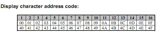
31 2-line display (N3=0,N = 1) (Figure 9) Case 1: When the number of display characters is less than 40 x 2 lines, the two lines are displayed from the head. Note that the first line end address and the second line start address are not consecutive. For example, when just the ST7036 is used, 20 characters x 2 lines are displayed. See Figure 9. When display shift operation is performed, the DDRAM address shifts. See Figure 10. Display Position DDRAM Address (hexadecimal) Fig. 9 2-Line Display Display Position DDRAM Address For Shift Left For Shift Right F F Fig Line by 20-Character Display Example 18/70
32 3-line display (N3=1,N =1) (Figure 11) Case 1: When the number of display characters is less than 16 x 3 lines, the tree lines are displayed from the head. For example, when just the ST7036 is used, 16 characters x 3 lines are displayed. See Figure 11. When display shift operation is performed, the DDRAM address shifts. See Figure 12. Display Position DDRAM Address (hexadecimal) D 0E 0F D 1E 1F D 2E 2F Fig Line Display Display Position DDRAM Address (hexadecimal) D 0E 0F D 1E 1F D 2E 2F E 0F 00 For Shift Left E 1F E 2F 20 For Shift Right F C 0D 0E 1F C 1D 1E 2F C 2D 2E Fig Line Display 19/70
33 Character Generator ROM (CGROM) The character generator ROM generates 5 x 8 dot character patterns from 8-bit character codes. It can generate 240/250/248/256 5 x 8 dot character patterns(select by OPR1/2 ITO pin). User-defined character patterns are also available by mask-programmed ROM. Character Generator RAM (CGRAM) In the character generator RAM, the user can rewrite character patterns by program. For 5 x 8 dots, eight character patterns can be written. Write into DDRAM the character codes at the addresses shown as the left column of Table 5 to show the character patterns stored in CGRAM. See Table 5 for the relationship between CGRAM addresses and data and display patterns. Areas that are not used for display can be used as general data RAM. ICON RAM In the ICON RAM, the user can rewrite icon pattern by program. There are totally 80 dots for icon can be written. See Table 6 for the relationship between ICON RAM address and data and the display patterns. Timing Generation Circuit The timing generation circuit generates timing signals for the operation of internal circuits such as DDRAM, CGROM and CGRAM. RAM read timing for display and internal operation timing by MPU access are generated separately to avoid interfering with each other. Therefore, when writing data to DDRAM, for example, there will be no undesirable interference, such as flickering, in areas other than the display area. LCD Driver Circuit(N3=0) LCD Driver circuit has 17 common and 100 segment signals for LCD driving. Data from CGRAM/CGROM/ICON is transferred to 100 bit segment latch serially, and then it is stored to 100 bit shift latch. When each common is selected by 17 bit common register, segment data also output through segment driver from 100 bit segment latch. In case of 1-line display mode, COM1 ~ COM8(with COMI) have 1/9 duty, and in 2-line mode, COM1 ~ COM16(with COMI) have 1/17 duty ratio. LCD Driver Circuit(N3=1) LCD Driver circuit has 25 common and 80 segment signals for LCD driving. Data from CGRAM/CGROM/ICON is transferred to 80 bit segment latch serially, and then it is stored to 80 bit shift latch. When each common is selected by 25 bit common register, segment data also output through segment driver from 80 bit segment latch. In case of 3-line display mode, COM1 ~ COM24(with COMI) have 1/25 duty. COM/SEG Output pins N3 COMI1 COM [1:8] VSS COMI1 COM [1:8] VDD NC COM [5:12] SEG [1:5] SEG [6:10] SEG [11:90] SEG [91:96] SEG SEG SEG SEG [1:5] [6:10] [11:90] [91:96] COM[4:1] SEG NC + COMI1 [1:80] NC Table 3. COM/SEG output define SEG [97:100] SEG [97:100] COM [13:16] COM [9:16] COM [9:16] COM [17:24] COMI2 COMI2 COMI2 Cursor/Blink Control Circuit It can generate the cursor or blink in the cursor/blink control circuit. The cursor or the blink appears in the digit at the display data RAM address set in the address counter. 20/70

34 Table 4 Correspondence between Character Codes and Character Patterns 21/70
=")
35 CGRAM/CGROM arrangement with (OPR1, OPR2)= 22/70
36 Character Code (DDRAM Data) CGRAM Address Character Patterns (CGRAM Data) b7 b6 b5 b4 b3 b2 b1 b0 b5 b4 b3 b2 b1 b0 b7 b6 b5 b4 b3 b2 b1 b Table 5 Relationship between CGRAM Addresses, Character Codes (DDRAM) and Character patterns (CGRAM Data) Notes: 1. Character code bits 0 to 2 correspond to CGRAM address bits 3 to 5 (3 bits: 8 types). 2. CGRAM address bits 0 to 2 designate the character pattern line position. The 8th line is the cursor position and its display is formed by a logical OR with the cursor. Maintain the 8th line data, corresponding to the cursor display position, at 0 as the cursor display. If the 8th line data is 1, 1 bits will light up the 8th line regardless of the cursor presence. 3. Character pattern row positions correspond to CGRAM data bits 0 to 4 (bit 4 being at the left). 4. As shown Table 5, CGRAM character patterns are selected when character code bits 4 to 7 are all 0. However, since character code bit 3 has no effect, the T display example above can be selected by either character code 00H or 08H for CGRAM data corresponds to display selection and 0 to non-selection, - Indicates no effect. 6. Different OPR1/2 ITO option can select different CGRAM size. 23/70
37 When ICON RAM data is filled the corresponding position displayed is described as the following table. When SHLS=1, ICON RAM map refer below table ICON Address ICON RAM bits D7~D5 D4 D3 D2 D1 D0 N3 = 0 N3 = 1 N3 = 0 N3 = 1 N3 = 0 N3 = 1 N3 = 0 N3 = 1 N3 = 0 N3 = 1 00H - S1/S81 S1 S2/S82 S2 S3/S83 S3 S4/S84 S4 S5/S85 S5 01H - S6/S86 S6 S7/S87 S7 S8/S88 S8 S9/S89 S9 S10/S90 S10 02H - S11/S91 S11 S12/S92 S12 S13/S93 S13 S14/S94 S14 S15/S95 S15 03H - S16/S96 S16 S17/S97 S17 S18/S98 S18 S19/S99 S19 S20/S100 S20 04H - S21 S21 S22 S22 S23 S23 S24 S24 S25 S25 05H - S26 S26 S27 S27 S28 S28 S29 S29 S30 S30 06H - S31 S31 S32 S32 S33 S33 S34 S34 S35 S35 07H - S36 S36 S37 S37 S38 S38 S39 S39 S40 S40 08H - S41 S41 S42 S42 S43 S43 S44 S44 S45 S45 09H - S46 S46 S47 S47 S48 S48 S49 S49 S50 S50 0AH - S51 S51 S52 S52 S53 S53 S54 S54 S55 S55 0BH - S56 S56 S57 S57 S58 S58 S59 S59 S60 S60 0CH - S61 S61 S62 S62 S63 S63 S64 S64 S65 S65 0DH - S66 S66 S67 S67 S68 S68 S69 S69 S70 S70 0EH - S71 S71 S72 S72 S73 S73 S74 S74 S75 S75 0FH - S76 S76 S77 S77 S78 S78 S79 S79 S80 S80 When SHLS=0, ICON RAM map refer below table ICON Address ICON RAM bits D7~D5 D4 D3 D2 D1 D0 N3 = 0 N3 = 1 N3 = 0 N3 = 1 N3 = 0 N3 = 1 N3 = 0 N3 = 1 N3 = 0 N3 = 1 00H - S100/S20 S80 S99/S19 S79 S98/S18 S78 S97/S17 S77 S96/S16 S76 01H - S95/S15 S75 S94/S14 S74 S93/S13 S73 S92S12 S72 S91/S11 S71 02H - S90/S10 S70 S89/S9 S69 S88/S8 S68 S87/S7 S67 S86/S6 S66 03H - S85/S5 S65 S84/S4 S64 S83/S3 S63 S82/S2 S62 S81/S1 S61 04H - S80 S60 S79 S59 S78 S58 S77 S57 S76 S56 05H - S75 S55 S74 S54 S73 S53 S72 S52 S71 S51 06H - S70 S50 S69 S49 S68 S48 S67 S47 S66 S46 07H - S65 S45 S64 S44 S63 S43 S62 S42 S61 S41 08H - S60 S40 S59 S39 S58 S38 S57 S37 S56 S36 09H - S55 S35 S54 S34 S53 S33 S52 S32 S51 S31 0AH - S50 S30 S49 S29 S48 S28 S47 S27 S46 S26 0BH - S45 S25 S44 S24 S43 S23 S42 S22 S41 S21 0CH - S40 S20 S39 S19 S38 S18 S37 S17 S36 S16 0DH - S35 S15 S34 S14 S33 S13 S32 S12 S31 S11 0EH - S30 S10 S29 S9 S28 S8 S27 S7 S26 S6 0FH - S25 S5 S24 S4 S23 S3 S22 S2 S21 S1 Table 6 ICON RAM map 24/70
38 Instructions There are four categories of instructions that: Designate ST7036 functions, such as display format, data length, etc. Set internal RAM addresses Perform data transfer with internal RAM Others instruction table at Normal mode (when EXT option pin connect to VDD, the instruction set follow below table) Instruction Clear Display Return Home Entry Mode Set Display ON/OFF Cursor or Display Shift Instruction Code RS R/W DB7 DB6 DB5 DB4 DB3 DB2 DB1 DB X I/D S D C B S/C R/L X X Description Write "20H" to DDRAM. and set DDRAM address to "00H" from AC Set DDRAM address to "00H" from AC and return cursor to its original position if shifted. The contents of DDRAM are not changed. Sets cursor move direction and specifies display shift. These operations are performed during data write and read. D=1:entire display on C=1:cursor on B=1:cursor position on Instruction Execution Time OSC= OSC= OSC= 380kHz 540kHz 700kHz 1.08 ms 1.08 ms 0.76 ms 0.76 ms 0.59 ms 0.59 ms 26.3 µs 18.5 µs 14.3 µs 26.3 µs 18.5 µs 14.3 µs S/C and R/L: Set cursor moving and display shift 26.3 µs 18.5 µs 14.3 µs control bit, and the direction, without changing DDRAM data. Function Set DL N X X X DL: interface data is 8/4 bits N: number of line is 2/ µs 18.5 µs 14.3 µs Set CGRAM AC5 AC4 AC3 AC2 AC1 AC0 Set DDRAM Address Read Busy Flag and Address Write Data to RAM Read Data from RAM AC6 AC5 AC4 AC3 AC2 AC1 AC0 0 1 BF AC6 AC5 AC4 AC3 AC2 AC1 AC0 1 0 D7 D6 D5 D4 D3 D2 D1 D0 1 1 D7 D6 D5 D4 D3 D2 D1 D0 Set CGRAM address in address counter Set DDRAM address in address counter Whether during internal operation or not can be known by reading BF. The contents of address counter can also be read. Write data into internal RAM (DDRAM/CGRAM) Read data from internal RAM (DDRAM/CGRAM) 26.3 µs 18.5 µs 14.3 µs 26.3 µs 18.5 µs 14.3 µs µs 18.5 µs 14.3 µs 26.3 µs 18.5 µs 14.3 µs Note: Be sure the ST7036 is not in the busy state (BF = 0) before sending an instruction from the MPU to the ST7036. If an instruction is sent without checking the busy flag, the time between the first instruction and next instruction will take much longer than the instruction time itself. Refer to Instruction Table for the list of each instruction execution time. 25/70
39 instruction table at Extension mode (when EXT option pin connect to VSS, the instruction set follow below table) Instruction Clear Display Return Home Entry Mode Set Display ON/OFF Instruction Code RS R/W DB7 DB6 DB5 DB4 DB3 DB2 DB1 DB x I/D S D C B Function Set DL N DH IS2 IS1 Set DDRAM Address Read Busy Flag and Address Write Data to RAM Read Data from RAM AC6 AC5 AC4 AC3 AC2 AC1 AC0 0 1 BF AC6 AC5 AC4 AC3 AC2 AC1 AC0 1 0 D7 D6 D5 D4 D3 D2 D1 D0 1 1 D7 D6 D5 D4 D3 D2 D1 D0 Description Write "20H" to DDRAM. and set DDRAM address to "00H" from AC Set DDRAM address to "00H" from AC and return cursor to its original position if shifted. The contents of DDRAM are not changed. Sets cursor move direction and specifies display shift. These operations are performed during data write and read. D=1:entire display on C=1:cursor on B=1:cursor position on DL: interface data is 8/4 bits N: number of line is 2/1 DH: double height font IS[2:1]: instruction table select Set DDRAM address in address counter Whether during internal operation or not can be known by reading BF. The contents of address counter can also be read. Write data into internal RAM (DDRAM/CGRAM/ICONRAM) Read data from internal RAM (DDRAM/CGRAM/ICONRAM) Instruction Execution Time OSC= OSC= OSC= 380kHz 540kHz 700kHz 1.08 ms 1.08 ms 0.76 ms 0.76 ms 0.59 ms 0.59 ms 26.3 µs 18.5 µs 14.3 µs 26.3 µs 18.5 µs 14.3 µs 26.3 µs 18.5 µs 14.3 µs 26.3 µs 18.5 µs 14.3 µs µs 18.5 µs 14.3 µs 26.3 µs 18.5 µs 14.3 µs 26/70
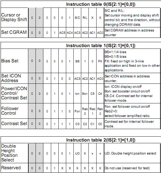
40 Cursor or Display Shift Instruction table 0(IS[2:1]=[0,0]) S/C R/L X X Set CGRAM AC5 AC4 AC3 AC2 AC1 AC0 S/C and R/L: Set cursor moving and display shift 26.3 µs 18.5 µs 14.3 µs control bit, and the direction, without changing DDRAM data. Set CGRAM address in address counter Instruction table 1(IS[2:1]=[0,1]) Bias Set BS 1 0 FX Set ICON Address Power/ICON Control/ Contrast Set Follower Control AC3 AC2 AC1 AC Ion Bon C5 C Fon Rab 2 Rab Contrast Set C3 C2 C1 C0 1 Rab µs 18.5 µs 14.3 µs BS=1:1/4 bias BS=0:1/5 bias FX: fixed on high in 3-line 26.3 µs 18.5 µs 14.3 µs application and fixed on low in other applications. Set ICON address in address counter. Ion: ICON display on/off Bon: set booster circuit on/off C5,C4: Contrast set for internal follower mode. Fon: set follower circuit on/off Rab2~0: select follower amplified ratio. Contrast set for internal follower mode µs 18.5 µs 14.3 µs 26.3 µs 18.5 µs 14.3 µs 26.3 µs 18.5 µs 14.3 µs 26.3 µs 18.5 µs 14.3 µs Double Height Position Select Instruction table 2(IS[2:1]=[1,0]) UD X x x UD: Double height position select 26.3 µs 18.5 µs 14.3 µs Reserved X X X X X X Do not use (reserved for test) 26.3 µs 18.5 µs 14.3 µs Instruction table 3(IS[2:1]=[1,1]):Do not use (reserved for test) 27/70
41 Instruction Description Clear Display RS R/W DB7 DB6 DB5 DB4 DB3 DB2 DB1 DB Clear all the display data by writing "20H" (space code) to all DDRAM address, and set DDRAM address to "00H" into AC (address counter). Return cursor to the original status, namely, bring the cursor to the left edge on first line of the display. Make entry mode increment (I/D = "1"). Return Home RS R/W DB7 DB6 DB5 DB4 DB3 DB2 DB1 DB X Return Home is cursor return home instruction. Set DDRAM address to "00H" into the address counter. Return cursor to its original site and return display to its original status, if shifted. Contents of DDRAM does not change. Entry Mode Set RS R/W DB7 DB6 DB5 DB4 DB3 DB2 DB1 DB I/D S Set the moving direction of cursor and display. I/D : Increment / decrement of DDRAM address (cursor or blink) When I/D = "High", cursor/blink moves to right and DDRAM address is increased by 1. When I/D = "Low", cursor/blink moves to left and DDRAM address is decreased by 1. * CGRAM operates the same as DDRAM, when read from or write to CGRAM. S: Shift of entire display When DDRAM read (CGRAM read/write) operation or S = "Low", shift of entire display is not performed. If S = "High" and DDRAM write operation, shift of entire display is performed according to I/D value (I/D = "1" : shift left, I/D = "0" : shift right). S I/D Description H H Shift the display to the left H L Shift the display to the right 28/70
42 Display ON/OFF RS R/W DB7 DB6 DB5 DB4 DB3 DB2 DB1 DB D C B Control display/cursor/blink ON/OFF 1 bit register. D : Display ON/OFF control bit When D = "High", entire display is turned on. When D = "Low", display is turned off, but display data is remained in DDRAM. C : Cursor ON/OFF control bit When C = "High", cursor is turned on. When C = "Low", cursor is disappeared in current display, but I/D register remains its data. B : Cursor Blink ON/OFF control bit When B = "High", cursor blink is on, that performs alternate between all the high data and display character at the cursor position. When B = "Low", blink is off. Alternating display Cursor Every 64 frames Cursor or Display Shift RS R/W DB7 DB6 DB5 DB S/C R/L DB3 DB2 DB1 DB0 X X S/C: Screen/Cursor select bit When S/C= High, Screen is controlled by R/L bit. When S/C= Low, Cursor is controlled by R/L bit. R/L: Right/Left When R/L= High, set direction to right. When R/L= Low, set direction to left. Without writing or reading of display data, shift right/left cursor position or display. This instruction is used to correct or search display data. During 2-line mode display, cursor moves to the 2nd line after 40th digit of 1st line. Note that display shift is performed simultaneously in all the line. When displayed data is shifted repeatedly, each line shifted individually. When display shift is performed, the contents of address counter are not changed. S/C R/L Description AC Value L L Shift cursor to the left AC=AC-1 L H Shift cursor to the right AC=AC+1 H L Shift display to the left. Cursor follows the display shift AC=AC H H Shift display to the right. Cursor follows the display shift AC=AC 29/70
43 Function Set RS R/W DB7 DB6 DB5 DB4 DB3 DB2 DB1 DB DL N DH IS2 IS1 DL : Interface data length control bit When DL = "High", it means 8-bit bus mode with MPU. When DL = "Low", it means 4-bit bus mode with MPU. So to speak, DL is a signal to select 8-bit or 4-bit bus mode. When 4-bit bus mode, it needs to transfer 4-bit data by two times. N : Display line number control bit When N = "High", 2-line display mode is set. When N = "Low", it means 1-line display mode. When N3 option pin connect to VDD, N must set N=1. DH : Double height font type control bit When DH = " High " and N= Low, display font is selected to double height mode(5x16 dot),ram address can only use 00H~27H. When DH= High and N= High, it is forbidden. When DH = " Low ", display font is normal (5x8 dot). N DH EXT option pin connect to high Character Display Lines Font EXT option pin connect to low Character Display Lines Font L L 1 5x8 1 5x8 L H 1 5x8 1 5x16 H L 2 5x8 2 5x8 H H 2 5x8 Forbidden 2 line mode normal display (DH=0/N=1) 1 line mode with double height font (DH=1/N=0) 30/70
44 IS[2:1]: instruction table select When IS[2:1]=(0,0): normal instruction be selected(refer instruction table 0) When IS[2:1]=(0,1):extension instruction be selected(refer instruction table 1 ) When IS[2:1]=(1,0):extension instruction be selected(refer instruction table 2 ) When IS[2:1]=(1,1):Do not use (reserved for test) Double height position set: IS[2:1]=(1,0) RS R/W DB7 DB6 DB5 DB4 DB3 DB UD X DB1 X DB0 X UD: Select double height font display position of screen.(n3=vdd) When UD = "High", double height font is show on Com1~Com16. RS R/W DB7 DB6 DB5 DB AC3 AC2 When UD = "Low", double height font is show on Com9~Com24. DB3 DB2 DB1 DB0 AC1 AC0 DH UD 2 LINES(N3=VSS) 3 LINES(N3=VDD) H H Com1~Com16 Double Height H L Com1~Com16 Double Height Com1~Com16 Double Height Com17~Com24 Normal Display Com1~Com8 Normal Display Com9~Com24 Double Height L X Normal Display Normal Display 31/70
45 3 Line mode normal display (DH = 0 / N = 1 / UD = don`t care ) COM1..8 is normal, COM is a double height font (DH = 1 / N = 1 / UD = 0 ) COM is normal, COM is a double height font (DH = 1 / N = 1 / UD = 1 ) 32/70
46 Set CGRAM Address RS R/W DB7 DB6 DB5 DB4 DB3 DB2 DB1 DB AC5 AC4 AC3 AC2 AC1 AC0 Set CGRAM address to AC. This instruction makes CGRAM data available from MPU. Set DDRAM Address RS R/W DB7 DB6 DB5 DB4 DB3 DB2 DB1 DB AC6 AC5 AC4 AC3 AC2 AC1 AC0 Set DDRAM address to AC. This instruction makes DDRAM data available from MPU. When 1-line display mode (N = 0), DDRAM address is from "00H" to "4FH". In 2-line display mode (N = 1), DDRAM address in the 1st line is from "00H" to "27H", and DDRAM address in the 2nd line is from "40H" to "67H". In 3-line display mode (N3=1, N=1), DDRAM address in the 1st line is from 00H to OFH, DDRAM in the 2nd line is from 10H to 1FH, and DDRAM in the 3rd line is from 20H to 2FH. Read Busy Flag and Address RS R/W DB7 DB6 DB5 DB4 DB3 DB2 DB1 DB0 0 1 BF AC6 AC5 AC4 AC3 AC2 AC1 AC0 When BF = High, indicates that the internal operation is being processed. So during this time the next instruction cannot be accepted. The address Counter (AC) stores DDRAM/CGRAM addresses, transferred from IR. After writing into (reading from) DDRAM/CGRAM, AC is automatically increased (decreased) by 1. Write Data to CGRAM,DDRAM or ICON RAM RS R/W DB7 DB6 DB5 DB4 DB3 DB2 DB1 DB0 1 0 D7 D6 D5 D4 D3 D2 D1 D0 Write binary 8-bit data to CGRAM,DDRAM or ICON RAM The selection of RAM from DDRAM, CGRAM or ICON RAM, is set by the previous address set instruction : DDRAM address set, CGRAM address set, ICON RAM address set. RAM set instruction can also determine the AC direction to RAM. After write operation, the address is automatically increased/decreased by 1, according to the entry mode. 33/70
47 Read Data from CGRAM,DDRAM or ICON RAM RS R/W DB7 DB6 DB5 DB4 DB3 DB2 DB1 DB0 1 1 D7 D6 D5 D4 D3 D2 D1 D0 Read binary 8-bit data from DDRAM/CGRAM./ICON RAM The selection of RAM is set by the previous address set instruction. If address set instruction of RAM is not performed before this instruction, the data that read first is invalid, because the direction of AC is not determined. If you read RAM data several times without RAM address set instruction before read operation, you can get correct RAM data from the second, but the first data would be incorrect, because there is no time margin to transfer RAM data. Bias Set BS: bias selection When BS= High, the bias will be 1/4 When BS= Low, the bias will be 1/5 BS will be invalid when external bias resistors are used(opf1=1,opf2=1) FX: must be fixed on high in 3-line application and fixed on low in other applications. Set ICON RAM address Set ICON RAM address to AC. This instruction makes ICON data available from MPU. When IS=1 at Extension mode, The ICON RAM address is from "00H" to "0FH". 34/70
48 Power/ICON control/contrast set(high byte) RS R/W DB7 DB6 DB5 DB4 DB3 DB ION BON DB1 C5 DB0 C4 Ion: set ICON display on/off When Ion = "High", ICON display on. When Ion = "Low", ICON display off. Bon: switch booster circuit Bon can only be set when internal follower is used (OPF1=0,OPF2=0). When Bon = "High", booster circuit is turn on. When Bon = "Low", booster circuit is turn off. C5,C4 : Contrast set(high byte) C5,C4,C3,C2,C1,C0 can only be set when internal follower is used (OPF1=0,OPF2=0).They can more precisely adjust the input reference voltage of V0 generator. The details please refer to the supply voltage for LCD driver. Follower control RS R/W DB7 DB6 DB5 DB DB3 FON DB2 Rab 2 DB1 Rab 1 DB0 Rab 0 Fon: switch follower circuit Fon can only be set when internal follower is used (OPF1=0,OPF2=0). When Fon = "High", internal follower circuit is turn on. When Fon = "Low", internal follower circuit is turn off. Note that Fon must be set to Low if (OPF1, OPF2) is not (0,0). Rab2,Rab1,Rab0 : V0 generator amplified ratio Rab2,Rab1,Rab0 can only be set when internal follower is used (OPF1=0,OPF2=0).They can adjust the amplified ratio of V0 generator. The details please refer to the supply voltage for LCD driver. Contrast set(low byte) RS R/W DB7 DB6 DB5 DB C3 C2 DB3 DB2 DB1 DB0 C1 C0 C3,C2,C1,C0:Contrast set(low byte) C5,C4,C3,C2,C1,C0 can only be set when internal follower is used (OPF1=0,OPF2=0).They can more precisely adjust the input reference voltage of V0 generator. The details please refer to the supply voltage for LCD driver. 35/70
49 Reset Function Initializing by Internal Reset Circuit An internal reset circuit automatically initializes the ST7036 when the power is turned on. The following instructions are executed during the initialization. The busy flag (BF) is kept in the busy state (BF = 1) until the initialization ends. The busy state lasts for 40 ms after VDD rises to stable. 1. Display clear 2. Function set: DL = 1; 8-bit interface data N = 0; 1-line display DH=0; normal 5x8 font IS[2:1]=(0,0); use instruction table 0 3. Display on/off control: D = 0; Display off C = 0; Cursor off B = 0; Blinking off 4. Entry mode set: I/D = 1; Increment by 1 S = 0; No shift 5. 3 line: FX=1 1/2 line: FX=0 6. ICON control Ion=0; ICON off 7. Power control BS=0; 1/5bias Bon=0; booster off Fon=0; follower off (C5,C4,C3,C2,C1,C0)=(1,0,0,0,0,0) (Rab2,Rab1,Rab0)=(0,1,0) 8. Double Height Position Select UD=0, double height font is show on Com9~Com24. Note: If the electrical characteristics conditions listed under the table Power Supply Conditions Using Internal Reset Circuit are not met, the internal reset circuit will not operate normally and will fail to initialize the ST7036. When internal Reset Circuit not operate,st7036 can be reset by XRESET pin from MPU control signal. 36/70
50 Initializing by Instruction 8-bit Interface (fosc=380khz) P O W E R O N o r e x te rn a l re s e t W a it tim e > 4 0 m S A fte r V D D s ta b le F u n c tio n s e t R S R /W D B 7 D B 6 D B 5 D B 4 D B 3 D B 2 D B 1 D B N D H IS 2 IS 1 B F c a n n o t b e c h e c k e d b e fo re th is in s tru c tio n. W a it tim e > μ S F u n c tio n s e t R S R /W D B 7 D B 6 D B 5 D B 4 D B 3 D B 2 D B 1 D B N D H IS 2 IS 1 B F c a n n o t b e c h e c k e d b e fo re th is in s tru c tio n. W a it tim e > μ S B ia s S e t R S R /W D B 7 D B 6 D B 5 D B 4 D B 3 D B 2 D B 1 D B B S 1 0 F X W a it tim e > μ S C o n tra s t s e t R S R /W D B 7 D B 6 D B 5 D B 4 D B 3 D B 2 D B 1 D B C 3 C 2 C 1 C 0 W a it tim e > μ S P o w e r/ic O N /C o n tra s t c o n tro l R S R /W D B 7 D B 6 D B 5 D B 4 D B 3 D B 2 D B 1 D B Io n B o n C 5 C 4 W a it tim e > μ S F o llo w e r c o n tro l R S R /W D B 7 D B 6 D B 5 D B 4 D B 3 D B 2 D B 1 D B F o n R a b 2 R a b 1 R a b 0 W a it tim e > μ S D is p la y O N /O F F c o n tro l R S R /W D B 7 D B 6 D B 5 D B 4 D B 3 D B 2 D B 1 D B D C B W a it tim e > μ S In itia liz a tio n e n d 37/70
51 Initial Program Code Example For 8051 MPU(8 Bit Interface): ; INITIAL_START: CALL DELAY40mS MOV A,#38H ;FUNCTION SET CALL WRINS_NOCHK ;8 bit, N=1,5*7dot CALL DELAY30uS MOV A,#38H ;FUNCTION SET CALL WRINS_NOCHK ;8 bit, N=1,5*7dot CALL DELAY30uS MOV A,#14H ;set bias CALL WRINS_CHK CALL DELAY30uS MOV A,#78H ;Contrast set adjustment CALL WRINS_CHK CALL DELAY30uS MOV A,#5EH ;Power/ICON/Contrast control CALL WRINS_CHK CALL DELAY30uS MOV A,#6AH ;Follower control CALL WRINS_CHK CALL DELAY30uS MOV A,#0CH ;DISPLAY ON CALL WRINS_CHK CALL DELAY30uS MOV A,#01H ;CLEAR DISPLAY CALL WRINS_CHK CALL DELAY2mS MOV A,#06H ;ENTRY MODE SET CALL WRINS_CHK ;CURSOR MOVES TO RIGHT CALL DELAY30uS ; MAIN_START: XXXX XXXX XXXX XXXX ; WRINS_CHK: CALL CHK_BUSY WRINS_NOCHK: CLR RS ;EX: Port 3.0 CLR RW ;EX: Port 3.1 SETB E ;EX:Port 3.2 MOV P1,A ;EX:Port 1=Data Bus CLR E MOV P1,#FFH ;For Check Busy Flag RET ; CHK_BUSY: ;Check Busy Flag CLR RS SETB RW SETB E JB P1.7,$ CLR E RET 38/70
52 4-bit Interface (fosc=380khz) 39/70
53 Initial Program Code Example For 8051 MPU(4 Bit Interface): ; INITIAL_START: CALL DELAY40mS MOV A,#30H ; FUNCTION SET CALL WRINS_ONCE ; 8 bit, DL = 1 CALL DELAY2mS MOV A,#30H ; FUNCTION SET CALL WRINS_ONCE ; 8 bit, DL = 1 CALL DELAY30uS MOV A,#30H ; FUNCTION SET CALL WRINS_ONCE ; 8 bit, DL = 1 CALL DELAY30uS CALL CHK_BUSY MOV A,#20H ; FUNCTION SET CALL WRINS_ONCE ; 4 bit, DL = 0 CALL DELAY30uS MOV A,#29H ; FUNCTION SET CALL WRINS_CHK ; 4 bit, DL = 0, N = 1, CALL DELAY30uS ; IS2 = 0, IS1 = 1 MOV A,#14H ;bias CALL WRINS_CHK CALL DELAY30uS MOV A,#78H ;Contrast set CALL WRINS_CHK CALL DELAY30uS MOV A,#5EH ;Power/ICON/Contrast CALL WRINS_CHK CALL DELAY30uS MOV A,#6AH ;Follower control CALL WRINS_CHK CALL DELAY30uS MOV A,#0CH ;DISPLAY ON CALL WRINS_CHK CALL DELAY30uS XXXX ; WRINS_CHK: CALL CHK_BUSY WRINS_NOCHK: PUSH A ANL A,#F0H CLR RS ;EX: Port 3.0 CLR RW ;EX: Port 3.1 SETB E ;EX: Port 3.2 MOV P1,A ;EX:Port1=Data Bus CLR E POP A SWAP A WRINS_ONCE: ANL A,#F0H CLR RS CLR RW SETB E MOV P1,A CLR E MOV P1,#FFH ;For Check Bus Flag RET ; CHK_BUSY: ;Check Busy Flag PUSH A MOV P1,#FFH $1 CLR RS SETB RW SETB E MOV A,P1 CLR E MOV P1,#FFH CLR RS SETB RW SETB E NOP CLR E JB A.7,$1 POP A RET MOV A,#01H ;CLEAR DISPLAY CALL WRINS_CHK CALL DELAY2mS MOV A,#06H ;ENTRY MODE SET CALL WRINS_CHK CALL DELAY30uS ; MAIN_START: XXXX XXXX XXXX 40/70
54 Serial interface & IIC interface ( fosc = 380kHz ) 41/70
55 Initial Program Code Example For 8051 MPU ( Serial Interface ) : ; INITIAL_START: CALL HARDWARE_RESET CALL DELAY40mS MOV A,#38H ;FUNCTION SET CALL WRINS_NOCHK ;8 bit, N=1,5*7dot CALL DELAY30uS MOV A,#39H ;FUNCTION SET CALL WRINS_NOCHK ;8 bit, N=1,5*7dot,IS=1 CALL DELAY30uS MOV A,#14H ;bias CALL WRINS_NOCHK CALL DELAY30uS MOV A,#78H ;Contrast set CALL WRINS_NOCHK CALL DELAY30uS MOV A,#5EH ;Power/ICON/Contrast control CALL WRINS_NOCHK CALL DELAY30uS MOV A,#6AH ;Follower control CALL WRINS_NOCHK CALL DELAY200mS ;for power stable MOV A,#0CH ;DISPLAY ON CALL WRINS_NOCHK CALL DELAY30uS MOV A,#01H ;CLEAR DISPLAY CALL WRINS_NOCHK CALL DELAY2mS MOV A,#06H ;ENTRY MODE SET CALL WRINS_NOCHK ;CURSOR MOVES TO RIGHT CALL DELAY30uS ; MAIN_START: XXXX XXXX XXXX XXXX... ; WRINS_NOCHK: PUSH 1 MOV R1,#8 CLR RS $1 RLC A MOV SI,C SETB SCL NOP CLR SCL DJNZ R1,$1 POP 1 CALL RET DLY1.5mS 42/70
56 Interfacing to the MPU The ST7036 can send data in two 4-bit operations/one 8-bit operation, serial 1 bit operation or fast I 2 C operation, thus allowing interfacing with 4-bit, 8-bit or I 2 C MPU. For 4-bit interface data, only four bus lines (DB4 to DB7) are used for transfer. Bus lines DB0 to DB3 are disabled. The data transfer between the ST7036 and the MPU is completed after the 4-bit data has been transferred twice. As for the order of data transfer, the four high order bits (for 8-bit operation, DB4 to DB7) are transferred before the four low order bits (for 8-bit operation, DB0 to DB3). The busy flag must be checked (one instruction) after the 4-bit data has been transferred twice. Two more 4-bit operations then transfer the busy flag and address counter data. Example of busy flag check timing sequence CSB RS R/W E Internal operation Functioning DB7 IR7 IR3 AC3 Not Busy AC3 IR7 IR3 Instruction write Busy flag check Busy flag check Instruction write Intel 8051 interface(4 Bit) P1.0 to P1.3 4 COM1 to COM16/24 DB4 to DB7 16/24 Intel 8051 Serial P3.0 P3.1 P3.2 RS R/W E P3.3 CSB ST7036 SEG1 to SEG100/80 100/80 43/70
57 For 8-bit interface data, all eight bus lines (DB0 to DB7) are used. Example of busy flag check timing sequence CSB RS R/W E Internal operation Functioning DB7 Data Busy Busy Not Busy Data Instruction write Busy flag check Busy flag check Busy flag check Instruction write Intel 8051 interface(8 Bit) P1.0 to P1.7 8 COM1 to COM16/24 DB0 to DB7 16/24 P3.0 P3.1 P3.2 P3.3 RS R/W E CSB SEG1 to SEG100/80 100/80 Intel 8051 Serial ST /70
58 For serial interface data, only two bus lines (DB6 to DB7) are used. Example of timing sequence CSB SI D7 D6 D5 D4 D3 D2 D1 D0 D7 D6 D5 D4 D3 D2 SCL RS Intel 8051 interface ( Serial 4-line ) P1.6 to P1.7 2 COM1 to COM16/24 SI, SCL 16/24 Intel 8051 Serial P3.0 P3.3 RS CSB ST7036 SEG1 to SEG100/80 100/80 45/70
59 For I 2 C interface data, all eight bus lines (DB0 to DB7) are used. Example of timing sequence SDA D7 D6 D5 D4 D3 D2 D1 D0 ACK D0 ACK SCL Intel 8051 interface ( I 2 C interface ) 46/70
60 Supply Voltage for LCD Drive When external bias resistors are used (OPF1=1,OPF2=1) VCC (2.7~ 5.5V) Vext VCC (2.7~ 5.5V) Vext OPF1 OPF2 VOUT VIN CAP1P CAP1N VDD V0 V1 V2 V3 V4 VSS VR R R R R VLCD OPF1 OPF2 VOUT VIN CAP1P CAP1N VDD V0 V1 V2 V3 V4 VSS VR R R R R VLCD 1/4 bias GND 1/5 bias GND When built-in bias resistors(9.6kω) are used (OPF1=1,OPF2=0) VCC(2.7~5.5V) Vext OPF1 VOUT VIN CAP1P CAP1N VDD V0 V1 V2 VR V3 VLCD V4 OPF2 VSS GND Note: Do not use built-in booster while built-in bias resistors are used. 47/70
61 When built-in bias resistors(3.3kω) are used (OPF1=0,OPF2=1) VCC (2.7~ 5.5V) Vext OPF2 VOUT VIN CAP1P CAP1N VDD V0 V1 V2 V3 V4 VR VLCD OPF1 VSS GND Note: Do not use built-in booster while built-in bias resistors are used. When built-in voltage followers with external Vout are used (OPF1=0,OPF2=0 and instruction setting Bon=0,Fon=1) Vext V0 VCC (2.7~ 5.5V) VOUT VIN CAP1P CAP1N VDD V0 V1 V2 V3 V4 Don't need to connect stable capacitor when use internal follower circuit VLCD OPF1 OPF2 VSS GND 48/70
62 When built-in booster and voltage followers are used(opf1=0,opf2=0) VIN VCC (2.7~ 3.5V) VDD Don't need to connect stable capacitor when use internal follower circuit VOUT CAP1P CAP1N V0 V1 V2 V3 V4 VLCD VOUT 2xVDD VDD=2.7~3.5V VSS=0V 2 x step-up voltage relationships OPF1 OPF2 VSS GND Note: Ensure V0 level stable, that must let Vout-V0 over 0.5V(if panel size over 4.5,the Vout-V0 propose over 0.8V). Vout Vout-V0 >0.5V(minimum) V0 VCC GND VDD VSS (System side) (ST7036Side) 49/70
63 V0 voltage follower value calculation VDD Vout( VDD) Vref Ra Rb V0 V0=(1+ Rb Ra ) x Vref While Vref=VDD x ( α ) VSS C5 C4 C3 C2 C1 C0 α Rab2 Rab1 Rab0 1+Rb/Ra : : : : V0 level (Condition:Booster on, Follower on, VIN=3.5V, VDD=3.0V,Display off) The recommended curve: follower = 04H Notes: 1. Vout V0 V1 V2 V3 V4 Vss must be maintained. 2. If the calculation value of V0 is higher than Vout, the real V0 value will saturate to Vout. 3. internal built-in booster can only be used when OPF1=0,OPF2=0. 50/70
64 V0 level (Condition: VDD=5.0V, external Vout=7.0V) The recommended curve: followe=01h Notes: 1. Vout V0 V1 V2 V3 V4 Vss must be maintained. 2. If the calculation value of V0 is higher than Vout, the real V0 value will saturate to Vout. 3. internal built-in booster can only be used when OPF1=0,OPF2=0. 51/70
65 AC Characteristics 68 Interface RS R/W taw6 tah6 CSB tcyc6 tewh tewl E tds6 tdh6 D0 to D7 (Write) tacc6 toh6 D0 to D7 (Read) Item Signal Symbol Condition ( Ta =-35 C to 85 C ) VDD=2.7 to 4.5V Rating VDD=4.5 to 5.5V Rating Units Min. Max. Min. Max. Address hold time RS tah Address setup time RS taw ns System cycle time RS tcyc ns Data setup time D0 to D7 tds Data hold time D0 to D7 tdh Access time D0 to D7 tacc CL = 100 pf Output disable time D0 to D7 toh ns ns Enable H pulse time E tewh ns Enable L pulse time E tewl ns Note: All timing is specified using 20% and 80% of VDD as the reference. 52/70
66 Serial Interface tcss tcsh CSB tsas tsah RS tscyc tslw tshw SCL tsds tsdh SI Item Signal Symbol Condition ( Ta =-35 C to 85 C ) VDD=2.7 to 4.5V Rating VDD=4.5 to 5.5V Rating Units Min. Max. Min. Max. Serial Clock Period tscyc SCL H pulse width SCL tshw SCL L pulse width tslw Address setup time tsas RS Address hold time tsah Data setup time tsds SI Data hold time tsdh CS-SCL time CS tcss tcsh ns ns ns ns *1 All timing is specified using 20% and 80% of VDD as the standard. 53/70
67 I2C interface SDA tbuf tlow thigh tsu;dat SCL SDA tdh;sta tr thd;dat tf tsu;sta tsu;sto Item Signal Symbol Condition ( Ta =-35 C to 85 C ) VDD=2.7 to 4.5V Rating VDD=4.5 to 5.5V Rating Units Min. Max. Min. Max. SCL clock frequency f SCLK DC 300K DC 400 khz SCL clock low period SCL t LOW µs SCL clock high period t HIGH Data set-up time t SU;DAT ns SDA Data hold time µs t HD:DAT SCL,SDA rise time SCL, t r C b C b 300 SCL,SDA fall time SDA t f C b C b 300 ns Capacitive load represent by each bus line C b pf Setup time for a repeated START condition SDA t SU;STA µs Start condition hold time t HD;STA µs Setup time for STOP condition t SU;STO µs Bus free time between a Stop and START condition SCL t BUF µs 54/70
68 Internal Power Supply Reset 2.7V/4.5V 0.2V 0.2V 0.2V trcc toff 0.1mS trcc 10mS toff 1mS Notes: toff compensates for the power oscillation period caused by momentary power supply oscillations. Specified at 4.5V for 5V operation, and at 2.7V for 3V operation. For if 2.7V/4.5V is not reached during 3V/5V operation, internal reset circuit will not operate normally. Hardware reset(xreset) tr 100nS 2.7V/4.5V 0.2V tl>100us 55/70
69 Absolute Maximum Ratings Characteristics Symbol Value Power Supply Voltage VDD -0.3 to +6.0 LCD Driver Voltage V LCD 7.0- Vss to -0.3+Vss Input Voltage V IN -0.3 to VDD+0.3 Operating Temperature T A -30 o C to + 85 o C Storage Temperature T STO -65 o C to o C DC Characteristics (VDD = 2.7 V, TA =-35 to 85 ) Symbol Characteristics Test Condition Min. Typ. Max. Unit VDD Operating Voltage V V LCD LCD Voltage V0-Vss V VIN Power Supply V I DD V IH1 Power Supply Current Input High Voltage (Except OSC1) VDD=3.0V (Use internal booster/follower circuit) ua 0.7 VDD - VDD V V IL1 Input Low Voltage (Except OSC1) V V IH2 Input High Voltage (OSC1) VDD - VDD V V IL2 Input Low Voltage (OSC1) VDD V V OH Output High Voltage (DB0 - DB7) I OH = -1.0mA 0.7 VDD - - V V OL Output Low Voltage (DB0 - DB7) I OL = 1.0mA V R COM Common Resistance V LCD = 4V, I d = 0.05mA KΩ R SEG Segment Resistance V LCD = 4V, I d = 0.05mA KΩ I LEAK Input Leakage Current V IN = 0V to VDD -1-1 µa I PUP Pull Up MOS Current VDD = 3V µa fosc Oscillation frequency VDD = 3V,1/17duty khz 56/70
70 DC Characteristics (VDD = 4.5 V,TA = -35 to 85 ) Symbol Characteristics Test Condition Min. Typ. Max. Unit VDD Operating Voltage V V LCD LCD Voltage V0-Vss V VIN Power Supply V I DD V IH1 Power Supply Current Input High Voltage (Except OSC1) VDD=5.0V (Use internal booster/follower circuit) µa 0.7 VDD - VDD V V IL1 Input Low Voltage (Except OSC1) V V IH2 Input High Voltage (OSC1) VDD - VDD V V IL2 Input Low Voltage (OSC1) V V OH Output High Voltage (DB0 - DB7) I OH = -1.0mA 0.8 VDD - VDD V V OL Output Low Voltage (DB0 - DB7) I OL = 1.0mA V R COM Common Resistance V LCD = 4V, I d = 0.05mA KΩ R SEG Segment Resistance V LCD = 4V, I d = 0.05mA KΩ I LEAK Input Leakage Current V IN = 0V to VDD -1-1 µa I PUP Pull Up MOS Current VDD = 5V µa fosc Oscillation frequency VDD = 5V,1/17duty khz 57/70
71 LCD Frame Frequency 1/16 Duty(ST7066U normal mode); Assume the oscillation frequency is 540KHZ, 1 clock cycle time = 1.85us, 1/16 duty; 1/5 bias,1 frame =1.85us x 200 x 16 = 5.92ms=168.9Hz(SHLC and SHLS connect to High) 200 clocks COM1 V0 V1 V2 V3 V4 Vss COM2 V0 V1 V2 V3 V4 Vss COM16 V0 V1 V2 V3 V4 Vss SEGx off V0 V1 V2 V3 V4 Vss SEGx on V0 V1 V2 V3 V4 Vss 1 frame 58/70
72 1/17 Duty(Extension mode); Assume the oscillation frequency is 540KHZ, 1 clock cycle time = 1.85us, 1/17 duty; 1/5 bias,1 frame =1.85us x 200 x 17 = 6.29ms=159Hz(SHLC and SHLS connect to High) 200 clocks COM1 V0 V1 V2 V3 V4 Vss COM2 V0 V1 V2 V3 V4 Vss COM17 V0 V1 V2 V3 V4 Vss SEGx off V0 V1 V2 V3 V4 Vss SEGx on V0 V1 V2 V3 V4 Vss 1 frame 59/70
73 1/8 Duty(ST7066U normal mode); Assume the oscillation frequency is 540KHZ, 1 clock cycle time = 1.85us, 1/8 duty; 1/4 bias,1 frame = 1.85us x 400 x 8 = 5.92ms=168.9Hz(SHLC and SHLS connect to High) 400 clocks V0 V1 COM1 V2 V3 V4 Vss V0 V1 COM2 V2 V3 V4 Vss V0 V1 COM8 V2 V3 V4 Vss V0 V1 SEGx off V2 V3 V4 Vss SEGx on V0 V1 V2 V3 V4 Vss 1 frame 60/70
74 1/9 Duty(Extension mode); Assume the oscillation frequency is 540KHZ, 1 clock cycle time = 1.85us, 1/9 duty; 1/4 bias,1 frame = 1.85us x 400 x 9 = 6.66ms=150Hz(SHLC and SHLS connect to High) 400 clocks V0 V1 COM1 V2 V3 V4 Vss V0 V1 COM2 V2 V3 V4 Vss V0 V1 COM9 V2 V3 V4 Vss V0 V1 SEGx off V2 V3 V4 Vss SEGx on V0 V1 V2 V3 V4 Vss 1 frame 61/70
75 1/25 Duty( Extension mode and 3-line ); Assume the oscillation frequency is 540KHZ, 1 clock cycle time = 1.85us, 1/25 duty; 1/4 bias,1 frame = 1.85us x 160 x 25 = 7.40ms=135.1Hz(SHLC and SHLS connect to High) 160 clocks V0 V1 COM1 V2 V3 V4 Vss V0 V1 COM2 V2 V3 V4 Vss V0 V1 COM25 V2 V3 V4 Vss V0 V1 SEGx off V2 V3 V4 Vss SEGx on V0 V1 V2 V3 V4 Vss 1 frame 62/70
76 I/O Pad Configuration 63/70


77 LCD and ST7036 Connection SHLC/SHLS ITO option pin can select at different direction for LCD panel Com normal direction/seg normal direction Com normal direction/seg reverse direction 3 line x 16 characters, SHLC=1 SHLS=1 Com reverse direction/seg normal direction 3 line x 16 characters, SHLC=1, SHLS=0 Com reverse direction/seg reverse direction 3 line x 16 characters, SHLC=0, SHLS=1 3 line x 16 characters, SHLC=0, SHLS=0 64/70
78 Application Circuit ( Normal mode ) Use internal resistor(9.6k ohm) and contrast adjust with external VR. Booster always off. Has 240 character of CGROM. Internal oscillator. Dot Matrix LCD Panel Vext VDD VOUT VIN CAP1N CAP1P V0 V1 V2 V3 V4 Com 1-24 ST7036 Seg 1-80 RS,R/W,E,CSB,DB0-DB7,XRESET CLS SHLC SHLS N3 EXT OPF1 OPF2 OPR1 OPR2 VDD To MPU 65/70
79 Application Circuit(Extension mode) Use internal follower circuit. Booster has 2 times pump. Has 240 character of CGROM. Internal oscillator. Dot M atrix LCD Panel Vext VDD VO UT VIN CAP1N CAP1P V0 V1 V2 V3 V4 Com 1-24 Seg 1-80 ST7036 RS,R/W,E,CSB,DB0-DB7,XRESET C LS SHLC SH LS N3 EXT O PF1 O PF2 O PR 1 O PR 2 To M PU When the heavy load is applied, the dotted line part could be added. 66/70


80 Application Circuit ( for glass layout ) ST7036 over Glass,6800 serial 8bit interface, with booster and follower circuit on 67/70
81 ST7036 over Glass,6800 serial 4bit interface, with booster and follower circuit on 68/70


82 ST7036 over Glass, serial interface, with booster and follower circuit on 69/70
83 ST7036 over Glass, I 2 C interface, with booster and follower circuit on In I2C application, note that the impedence of SDAs and GNDs should be keep in the POWER PIN LEVEL. 70/70
844-8795 Fax:")
84 User s Guide LCD Safe Handling Procedure For product support, contact Newhaven Display International 2511 Technology Drive, #101 Elgin, IL Tel: (847) Fax: (847)
NHD C0220BiZ FS(RGB) FBW 3VM
 FBW 3VM") NHD C0220BiZ FS(RGB) FBW 3VM COG (Chip On Glass) Character Liquid Crystal Display Module NHD Newhaven Display C0220 COG 2 lines x 20 characters BiZ Model, with I2C interface F Transflective S(RGB) Side
NHD C0220BiZ FS(RGB) FBW 3VM COG (Chip On Glass) Character Liquid Crystal Display Module NHD Newhaven Display C0220 COG 2 lines x 20 characters BiZ Model, with I2C interface F Transflective S(RGB) Side
NHD-C0220BiZ-FS(RGB)-FBW-3VM
-FBW-3VM") NHD-C0220BiZ-FS(RGB)-FBW-3VM COG (Chip-On-Glass) Character Liquid Crystal Display Module NHD- Newhaven Display C0220- COG, 2 Lines x 20 Characters BiZ- Model, I 2 C Interface F- Transflective S(RGB)- Side
NHD-C0220BiZ-FS(RGB)-FBW-3VM COG (Chip-On-Glass) Character Liquid Crystal Display Module NHD- Newhaven Display C0220- COG, 2 Lines x 20 Characters BiZ- Model, I 2 C Interface F- Transflective S(RGB)- Side
Sitronix. ST7038i FEATURES GENERAL DESCRIPTION. Dot Matrix LCD Controller/Driver
 ST Sitronix FEATURES 5 x 8 dot matrix possible Support low voltage single power operation: VDD, VDD2: 1.8 to 3.3V (typical) LCD Voltage Operation Range (V0/Vout) Programmable V0: 3 to 7V(V0) External power
NHD-C0216CiZ-FSW-FBW-3V3
 NHD-C0216CiZ-FSW-FBW-3V3 COG (Chip-on-Glass) Liquid Crystal Display Module NHD- Newhaven Display C0216- COG, 2 lines x 16 characters CiZ- Model F- Transflective SW- Side White LED Backlight F- FSTN (+)
NHD-C0216CiZ-FSW-FBW-3V3
 NHD-C0216CiZ-FSW-FBW-3V3 COG (Chip-on-Glass) Liquid Crystal Display Module NHD- Newhaven Display C0216- COG, 2 Lines x 16 Characters CiZ- Model F- Transflective SW- Side White LED Backlight F- FSTN (+)
6800-4bit / 8bit, 4-Line interface (without IIC interface)
") ST Sitronix ST7032 Dot Matrix LCD Controller/Driver Features 5 x 8 dot matrix possible Low power operation support: -- 2.7 to 5.5V Range of LCD driver power -- 3.0 to 7.0V 4-bit, 8-bit, serial MPU or 400kbits/s
ST Sitronix ST7032 Dot Matrix LCD Controller/Driver Features 5 x 8 dot matrix possible Low power operation support: -- 2.7 to 5.5V Range of LCD driver power -- 3.0 to 7.0V 4-bit, 8-bit, serial MPU or 400kbits/s
NHD-C0216CZ-FSW-FBW-3V3
 NHD-C0216CZ-FSW-FBW-3V3 COG (Chip-on-Glass) Liquid Crystal Display Module NHD- Newhaven Display C0216- COG, 2 Lines x 16 Characters CZ- Model F- Transflective SW- Side White LED Backlight F- FSTN (+) B-
NHD C12864MZ NSW BTW. COG (Chip On Glass) Liquid Crystal Display Module
 Liquid Crystal Display Module") NHD C12864MZ NSW BTW COG (Chip On Glass) Liquid Crystal Display Module NHD Newhaven Display C12864 128 x 64 pixels MZ Model N Transmissive SW Side White LED backlight B STN Blue ( ) T 12:00 view W Wide
NHD C12864MZ NSW BTW COG (Chip On Glass) Liquid Crystal Display Module NHD Newhaven Display C12864 128 x 64 pixels MZ Model N Transmissive SW Side White LED backlight B STN Blue ( ) T 12:00 view W Wide
中显液晶 技术资料 中显控制器使用说明书 2009年3月15日 北京市海淀区中关村大街32号和盛大厦811室 电话 86 010 52926620 传真 86 010 52926621 企业网站.zxlcd.com
 http://wwwzxlcdcom 4 SEG / 6 COM DRIVER & CONTROLLER FOR DOT MATRIX LCD June 2 Ver Contents in this document are subject to change without notice No part of this document may be reproduced or transmitted
Newhaven Display International, Inc Galvin Ct. Elgin IL, Ph: Fax:
 NHD-0108HZ-FSW-GBW Character Liquid Crystal Display Module NHD- Newhaven Display 0108-1 Line x 8 Characters HZ- Model F- Transflective SW- Side White LED Backlight G- STN- Gray B- 6:00 Optimal View W-
COG (Chip-on-Glass) Liquid Crystal Display Module
 Liquid Crystal Display Module") NHD-C0220AZ-FSW-FTW COG (Chip-on-Glass) Liquid Crystal Display Module NHD- Newhaven Display C0220- COG, 2 Lines x 20 Characters AZ- Model F- Transflective SW- Side White LED Backlight F- FSTN Positive
NHD-C0220AZ-FSW-FTW COG (Chip-on-Glass) Liquid Crystal Display Module NHD- Newhaven Display C0220- COG, 2 Lines x 20 Characters AZ- Model F- Transflective SW- Side White LED Backlight F- FSTN Positive
16COM/40SEG DRIVER & CONTROLLER FOR DOT MATRIX LCD
 6COM/4SEG DRIVER & CONTROLLER FOR DOT MATRIX LCD INTRODUCTION is a dot matrix LCD driver & controller LSI which is fabricated by low power CMOS technology It can display, 2-line with 5 x 8 or 5 x dots
NHD 0216K1Z NS(RGB)FBW REV1
FBW REV1") NHD 0216K1Z NS(RGB)FBW REV1 Character Liquid Crystal Display Module NHD Newhaven Display 0216 2 lines x 16 characters K1Z Model NS Transmissive ( ) RGB Side backlight RED, GREEN, BLUE F FSTN ( ) B 6:00
NHD 0216K1Z NS(RGB)FBW REV1 Character Liquid Crystal Display Module NHD Newhaven Display 0216 2 lines x 16 characters K1Z Model NS Transmissive ( ) RGB Side backlight RED, GREEN, BLUE F FSTN ( ) B 6:00
NHD-C12864WC-FSW-FBW-3V3
 NHD-C12864WC-FSW-FBW-3V3 COG (Chip-On-Glass) Liquid Crystal Display Module NHD- Newhaven Display C12864-128 x 64 Pixels WM- Model F- Transflective SW- Side White LED Backlight F- FSTN (+) B- 6:00 Optimal
16COM/80SEG DRIVER & CONTROLLER FOR DOT MATRIX LCD
 6COM/80SEG DRIVER & CONTROLLER FOR DOT MATRIX LCD INTRODUCTION The is a dot matrix LCD driver & controller LSI which is fabricated by low power CMOS technology It is capable of displaying or 2 lines with
NHD WG AFFH TZ#001 C
 NHD 320240WG AFFH TZ#001 C Graphic Liquid Crystal Display Module NHD Newhaven Display 320240 320 x 240 pixels WG Display Type: Graphic A Model F White CCFL Backlight F FSTN (+) H Transflective, 6:00 view,
Contents. 1. Revision History
 Address: Midas Components Ltd, Electra House, 32 Southtown Road, Great Yarmouth, Norfolk, England, NR31 ODU Email:sales@midascomponents.co.uk Website:www.midascomponents.co.uk Tel:+44(0)1493 602602 Fax:+44(0)1493
NHD WG BTML VZ#
 NHD 240128WG BTML VZ# Graphic Liquid Crystal Display Module NHD Newhaven Display 240128 240 x 128 pixels WG Display Type: Graphic B Model T White LED backlight M STN Blue ( ) L Transmissive, 12:00 View,
 NHD Newhaven Display 0220 2 Lines x 20 Characters WH Display Type: Character M Model T White LED Backlight F FSTN (+) White H Transflective, 6:00 Optimal View JT# English and Japanese Standard Font E ESD
COG (Chip-on-Glass) Liquid Crystal Display Module
 Liquid Crystal Display Module") NHD-C0216AZ-FSW-GBW COG (Chip-on-Glass) Liquid Crystal Display Module NHD- Newhaven Display C0216- COG, 2 Lines x 16 Characters AZ- Model F- Transflective SW- Side White LED Backlight G- STN- Gray B- 6:00
NHD-C0216AZ-FSW-GBW COG (Chip-on-Glass) Liquid Crystal Display Module NHD- Newhaven Display C0216- COG, 2 Lines x 16 Characters AZ- Model F- Transflective SW- Side White LED Backlight G- STN- Gray B- 6:00
NHD BZ NSW BTW 3V3
 NHD 240128BZ NSW BTW 3V3 Graphic Liquid Crystal Display Module NHD Newhaven Display 240128 240 x 128 pixels BZ Model N Transmissive SW Side White LED Backlight B STN Blue ( ) T 12:00 view W Wide Temperature
LCM NHD-0440CI-YTBL. User s Guide. (Liquid Crystal Display Module) RoHS Compliant. For product support, contact NHD CI- Y- T- B- L-
 RoHS Compliant. For product support, contact NHD CI- Y- T- B- L-") User s Guide NHD-0440CI-YTBL LCM (Liquid Crystal Display Module) RoHS Compliant NHD- 0440- CI- Y- T- B- L- Newhaven Display 4 Lines x 40 Characters C: Display Series/Model I: Factory line STN Yellow/Green
User s Guide NHD-0440CI-YTBL LCM (Liquid Crystal Display Module) RoHS Compliant NHD- 0440- CI- Y- T- B- L- Newhaven Display 4 Lines x 40 Characters C: Display Series/Model I: Factory line STN Yellow/Green
Newhaven Display International, Inc Galvin Ct. Elgin IL, Ph: Fax:
 NHD-0220WH-MTGH-JT#E Character Liquid Crystal Display Module NHD- Newhaven Display 0220-2 Lines x 20 Characters WH- Display Type: Character M- Model T- White LED Backlight G- STN- Gray H- Transflective,
onlinecomponents.com
 NHD 240128WG ATFH VZ# Graphic Liquid Crystal Display Module NHD Newhaven Display 240128 240 x 128 pixels WG Display Type: Graphic A Model T White LED Backlight F FSTN (+) H Transflective, 6:00 view, Wide
Midas LCD Part Number System
 Address: Midas Components Ltd, Electra House, 32 Southtown Road, Great Yarmouth, Norfolk, England, NR31 ODU Email:sales@midascomponents.co.uk Website:www.midascomponents.co.uk Tel:+44(0)1493 602602 Fax:+44(0)1493
16COM / 40SEG DRIVER & CONTROLLER FOR DOT MATRIX LCD
 INTRODUCTION KS0066U is a dot matrix LCD driver & controller LSI whichis fabricated by low power CMOS technology It can display 1or 2 lines with the 5 8 dots format or 1 line with the 5 11 dots format
NHD WG BoTML VZ# 030
 NHD 320240WG BoTML VZ# 030 Graphic Liquid Crystal Display Module NHD Newhaven Display 320240 320 x 240 pixels WG Display Type: Graphic Bo Model T White LED Backlight M STN Negative Blue L Transmissive,
NHD ZF CTXL#
 NHD 1.8 128160ZF CTXL# TFT (Thin Film Transistor) Liquid Crystal Display Module NHD Newhaven Display 1.8 1.8 diagonal 128160 128 x 160 pixels (portrait mode) ZF Model C Built in Controller T White LED
NHD 24064WG ASFH VZ# Graphic Liquid Crystal Display Module
 NHD 24064WG ASFH VZ# Graphic Liquid Crystal Display Module NHD Newhaven Display 24064 240 x 64 pixels WG Display Type: Graphic A Model S Super Bright White LED Backlight F FSTN (+) H Transflective, 6:00
NHD-C12864LZ-FSW-FBW-3V3
 NHD-C12864LZ-FSW-FBW-3V3 COG (Chip-On-Glass) Liquid Crystal Display Module NHD- Newhaven Display C12864-128 x 64 Pixels LZ- Model F- Transflective SW- Side White LED backlight F- FSTN (+) B- 6:00 Optimal
NHD 0216K3Z FL GBW. Serial Liquid Crystal Display Module
 NHD 0216K3Z FL GBW Serial Liquid Crystal Display Module NHD Newhaven Display 0216 2 lines x 16 characters K3Z Model F Transflective L Yellow/Green LED backlight G STN Gray B 6:00 view W Wide Temperature
NHD-C12832A1Z-NSW-BBW-3V3
 NHD-C12832A1Z-NSW-BBW-3V3 COG (Chip-On-Glass) Liquid Crystal Display Module NHD- Newhaven Display C12832-128 x 32 Pixels A1Z- Model N- Transmissive SW- Side White LED Backlight B- STN Negative, Blue B-
16COM / 80SEG DRIVER & CONTROLLER FOR DOT MATRIX LCD
 INTRODUCTION KS0070B is a dot matrix LCD driver & controller LSI which is fabricated by low power CMOS technology. It is capable of displaying 1 or 2 lines with the 5 7 format or 1 line with the 5 10 dots
NHD-0216K3Z-NS(RGB)-FBW-V3
-FBW-V3") NHD-0216K3Z-NS(RGB)-FBW-V3 Serial Liquid Crystal Display Module NHD- Newhaven Display 0216-2 Lines x 16 Characters K3Z- Model N- Transmissive S(RGB)- Side LED Backlights (Red-Green-Blue) F- FSTN(-) B-
NHD-0216K3Z-NS(RGB)-FBW-V3 Serial Liquid Crystal Display Module NHD- Newhaven Display 0216-2 Lines x 16 Characters K3Z- Model N- Transmissive S(RGB)- Side LED Backlights (Red-Green-Blue) F- FSTN(-) B-
NHD WX CoTFH V#I041
 NHD 320240WX CoTFH V#I041 Graphic Liquid Crystal Display Module NHD Newhaven Display 320240 320 x 240 pixels WX Display Type: Graphic Co Model T White LED Backlight F FSTN (+) H Transflective, 6:00 view,
Newhaven Display International, Inc Technology Drive, Suite 101 Elgin IL, Ph: Fax:
 NHD 24064WG ATFH VZ# Graphic Liquid Crystal Display Module NHD Newhaven Display 24064 240 x 64 pixels WG Display Type: Graphic A Model T White LED Backlight F FSTN (+) H Transflective, 6:00 view, Wide
NHD-C12864LZ-FSW-FBW-3V3
 NHD-C12864LZ-FSW-FBW-3V3 COG (Chip-On-Glass) Liquid Crystal Display Module NHD- Newhaven Display C12864-128 x 64 Pixels LZ- Model F- Transflective SW- Side White LED backlight F- FSTN (+) B- 6:00 Optimal
Newhaven Display International, Inc Technology Drive, Suite 101 Elgin IL, Ph: Fax:
 NHD 24064WG ATMI VZ# Graphic Liquid Crystal Display Module NHD Newhaven Display 24064 240 x 64 pixels WG Display Type: Graphic A Model T White LED Backlight M STN Blue ( ) I Transmissive, 6:00 view, Wide
Newhaven Display International, Inc Galvin Dr. Elgin IL, Ph: Fax:
 NHD-24064WG-ATFH-VZ# Graphic Liquid Crystal Display Module NHD- Newhaven Display 24064-240 x 64 Pixels WG- Display Type: Graphic A- Model T- White LED Backlight F- FSTN Positive H- Transflective, 6:00
Newhaven Display International, Inc Galvin Ct. Elgin IL, Ph: Fax:
 NHD-12864WX-T1TFH# Graphic Liquid Crystal Display Module NHD- Newhaven Display 12864-128 x 64 Pixels WX- Display Type: Graphic, Tab Type T1- Model T- White LED Backlight F- FSTN (+) H- Transflective, Wide
NHD-0220D3Z-FL-GBW-V3
 NHD-0220D3Z-FL-GBW-V3 Serial Liquid Crystal Display Module NHD- Newhaven Display 0220-2 Lines x 20 Characters D3Z- Model F- Transflective L- Yellow/Green LED Backlight G- STN-Gray B- 6:00 Optimal View
LCM NHD-0440AZ-FSW -FBW. User s Guide. (Liquid Crystal Display Character Module) RoHS Compliant FEATURES
 RoHS Compliant FEATURES") User s Guide NHD-0440AZ-FSW -FBW LCM (Liquid Crystal Display Character Module) RoHS Compliant FEATURES Display format: 4 Lines x 40 Characters (A) Display Series/Model (Z) Factory line (F) Polarizer =
User s Guide NHD-0440AZ-FSW -FBW LCM (Liquid Crystal Display Character Module) RoHS Compliant FEATURES Display format: 4 Lines x 40 Characters (A) Display Series/Model (Z) Factory line (F) Polarizer =
NHD-0220D3Z-FL-GBW-V3
 NHD-0220D3Z-FL-GBW-V3 Serial Liquid Crystal Display Module NHD- Newhaven Display 0220-2 Lines x 20 Characters D3Z- Model F- Transflective L- Yellow/Green LED Backlight G- STN Positive - Gray B- 6:00 Optimal
NHD WG-BxTGH-VZ#-3VR
 NHD-320240WG-BxTGH-VZ#-3VR Graphic Liquid Crystal Display Module NHD- Newhaven Display 320240-320 x 240 Pixels WG- Display Type: Graphic Bx- Model T- White LED Backlight G- STN - Gray H- Transflective,
NHD SF CTXI# 1
 NHD 2.4 240320SF CTXI# 1 TFT (Thin Film Transistor) Liquid Crystal Display Module NHD Newhaven Display 2.4 2.4 diagonal 240320 240 x 320 pixels (portrait mode) SF Model C Built in Controller T White LED
NHD 0216KZW AB5. OLED Display Module
 NHD0216KZWAB5 OLED Display Module NHD Newhaven Display 0216 2 lines x 16 characters KZW OLED A Model B Emitting Color: Blue 5 +5V power supply Newhaven Display International, Inc 2511 Technology Drive,
34COM/60SEG DRIVER & CONTROLLER FOR DOT MATRIX LCD
 34COM/6SEG DRIVER & CONTROLLER FOR DOT MATRIX LCD INTRODUCTION is a dot matrix LCD driver & controller LSI which is fabricated by low power CMOS technology It can display, 2 or 4 lines with 5 8 or 6 8
Newhaven Display International, Inc Galvin Ct. Elgin IL, Ph: Fax:
 NHD-24064WG-ATMI-VZ# Graphic Liquid Crystal Display Module NHD- Newhaven Display 24064-240 x 64 Pixels WG- Display Type: Graphic A- Model T- Side White LED Backlight M- STN- Blue (-) I- Transmissive, 6:00
Newhaven Display International, Inc Galvin Ct. Elgin IL, Ph: Fax:
 NHD-12232AZ-FSW-GBW Graphic Liquid Crystal Display Module NHD- Newhaven Display 12232-122 x 32 Pixels AZ- Model F- Transflective SW- Side White LED Backlight G- STN Positive, Gray B- 6:00 Optimal View
Newhaven Display International, Inc Galvin Ct. Elgin IL, Ph: Fax:
 NHD0420DZWAB5 Character OLED Display Module NHD Newhaven Display 0420 4 lines x 20 characters DZW OLED A Model B Emitting Color: Blue 5 +5V power supply Newhaven Display International, Inc 2661 Galvin
NHD-C12864LZ-NSW-FBW-3V3
 NHD-C12864LZ-NSW-FBW-3V3 COG (Chip-On-Glass) Liquid Crystal Display Module NHD- Newhaven Display C12864-128 x 64 Pixels LZ- Model N- Transmissive SW- Side White LED Backlight F- FSTN, Negative B- 6:00
ST Sitronix ST7565R. 65 x 132 Dot Matrix LCD Controller/Driver. Ver 1.3 1/ /11/25
 ST Sitronix ST7565R 65 x 32 Dot Matrix LCD Controller/Driver Features Direct display of RAM data through the display data RAM. RAM capacity : 65 x 32 = 8580 bits Display duty selectable by select pin /65
NHD WG-BxTGH-VZ#-3VR
 NHD-320240WG-BxTGH-VZ#-3VR Graphic Liquid Crystal Display Module NHD- Newhaven Display 320240-320 x 240 Pixels WG- Display Type: Graphic Bx- Model T- White LED Backlight G- STN - Gray H- Transflective,
RW1062 INTRODUCTION FUNCTIONS FEATURES. Crystalfontz. Thiscontrolerdatasheetwasdownloadedfrom htp:/www.crystalfontz.
 Crystalfontz Thiscontrolerdatasheetwasdownloadedfrom htp:/www.crystalfontz.com/controlers/ RW1062 INTRODUCTION RW1062 is a LCD driver & controller LSI which is fabricated by low power CMOS technology.
NHD MF 22 Controller Board
 NHD 3.5 320240MF 22 Controller Board TFT Controller Evaluation Board NHD Newhaven Display 3.5 3.5 Diagonal 320240 320xRGBx240 pixels MF Model 22 22 POS FFC interface (8 bit data) SSD1963 Controller Newhaven
ST Sitronix ST7565R. 65 x 132 Dot Matrix LCD Controller/Driver. Ver 1.7 1/ /06/01
 ST Sitronix ST7565R 65 x 32 Dot Matrix LCD Controller/Driver Features Directly display RAM data through Display Data RAM. RAM capacity : 65 x 32 = 8580 bits Display duty selectable by select pin /65 duty
SSD1803. Product Preview. 100 x 34 STN LCD Segment / Common Mono Driver with Controller
 SOLOMON SYSTECH SEMICONDUCTOR TECHNICAL DATA Crystalfontz Thiscontrolerdatasheetwasdownloadedfrom htp:/www.crystalfontz.com/controlers/ SSD1803 Product Preview 100 x 34 STN LCD Segment / Common Mono Driver
Parallel Display Specifications Revision 1.0
 MOP-AL162A Parallel Display Specifications Revision 1.0 Revision History Revision Description Author 1.0 Initial Release Clark 0.2 Updates as per issue #333 Clark 0.1 Initial Draft Clark 1 Contents Revision
NHD MF 22 Controller Board
 NHD 4.3 480272MF 22 Controller Board TFT Controller Evaluation Board NHD Newhaven Display 4.3 4.3 Diagonal 480272 480xRGBx272 pixels MF Model 22 22 POS FFC interface (8 bit data) SSD1963 Controller Newhaven
Item Symbol Standard Unit Power voltage VDD-VSS Input voltage VIN VSS - VDD
 SPECIFICATIONS OF LCD MODULE Features 1. 5x8 dots with cursor 2. Built-in controller (S6A0069 or equivalent) 3. Easy interface with 4-bit or 8-bit MPU 4. +5V power supply (also available for =3.0V) 5.
Newhaven Display International, Inc Galvin Ct. Elgin IL, Ph: Fax:
 NHD-0216AW-IB3 Character OLED Display Module NHD- Newhaven Display 0216-2 lines x 16 characters AW- Character OLED Module I- Model B- Blue 3-2.4V~5.5V Supply Voltage Newhaven Display International, Inc.
NHD C0216CZ FSW FBW 3V3
 NHD C0216CZ FSW FBW 3V3 COG (Chip on Glass) Liquid Crystal Display Module NHD Newhaven Display C0216 COG, 2 lines x 16 characters CZ Model F Transflective SW Side White LED Backlight F FSTN (+) B 6:00
NHD WG-ATMI-VZ#
 NHD-240128WG-ATMI-VZ# Graphic Liquid Crystal Display Module NHD- Newhaven Display 240128-240 x 128 Pixels WG- Display Type: Graphic A- Model T- White LED Backlight M- STN Negative, Blue I- Transmissive,
JUL. 27, 2001 Version 1.0
 S SPLC782A 6COM/8SEG Controller/Driver JUL. 27, 2 Version. SUNPLUS TECHNOLOGY CO. reserves the right to change this documentation without prior notice. Information provided by SUNPLUS TECHNOLOGY CO. is
68 x 102 Dot Matrix LCD Controller/Driver 1. INTRODUCTION
 Sitronix ST ST7579 68 x 102 Dot Matrix LCD Controller/Driver 1. INTRODUCTION The ST7579 is a driver & controller LSI for graphic dot-matrix liquid crystal display systems. It contains 102 segment and 67
Newhaven Display International, Inc Galvin Ct. Elgin IL, Ph: Fax:
 NHD0216SZWBY5 OLED Display Module NHD Newhaven Display 0216 2 Lines x 16 Characters SZW OLED B Model Y Emitting Color: Yellow 5 +5V Power Supply Newhaven Display International, Inc 2661 Galvin Ct Elgin
USER S GUIDE ATM4004A
 USER S GUIDE ATM4004A Liquid Crystal Display Module CONTENTS 1.0 Mechanical Diagram. 3 2.0 Absolute Maximum Ratings 4 3.0 Description of Terminals. 4 4.0 Optical Characteristics 5 5.0 Electrical Characteristics
ST Sitronix ST7565P. 65 x 132 Dot Matrix LCD Controller/Driver
 ST Sitronix ST7565P 65 x 132 Dot Matrix LCD Controller/Driver FEATURES Direct display of RAM data through the display data RAM. RAM capacity : 65 x 132 = 8580 bits Display duty selectable by select pin
NHD WG-ATFH-VZ#
 NHD-240128WG-ATFH-VZ# Graphic Liquid Crystal Display Module NHD- Newhaven Display 240128-240 x 128 Pixels WG- Display Type: Graphic A- Model T- White LED Backlight F- FSTN (+) H- Transflective, 6:00 Optimal
NHD EF-CTXI#
 NHD-1.8-128160EF-CTXI# TFT (Thin-Film Transistor) Liquid Crystal Display Module NHD- Newhaven Display 1.8-1.8 Diagonal 128160-128 x 160 Pixels (Portrait Mode) EF- Model C- Built-in Controller T- White
SPECIFICATIONS FOR LCD MODULE
 SPECIFICATIONS FOR LCD MODULE CUSTOMER CUSTOMER PART NO. ORIENT DISPLAY NO. OD-AMC162A SERIES DESCRIPTION APPROVED BY DATE PREPARED BY CHECKED BY APPROVED BY PAGE 1 OF 23 DOCUMENT REVISION HISTORY: DATE
AZ DISPLAYS, INC. COMPLETE LCD SOLUTIONS SPECIFICATIONS FOR LIQUID CRYSTAL DISPLAY
 AZ DISPLAYS, INC. COMPLETE LCD SOLUTIONS SPECIFICATIONS FOR LIQUID CRYSTAL DISPLAY PART NUMBER: ACM1602B (WHITE EDGELIGHT) SERIES DATE: APRIL 28, 2003 1.0 MECHANICAL SPECS 1. Overall Module Size 84.0mm(W)
LCD Module User Manual
 LCD Module User Manual Customer : MASS PRODUCTION CODE DRAWING NO : TC1602D-02WA0 : m-tc1602d-02wa0_a00 Approved By Customer: Date: Approved By Checked By Prepared By Vatronix Holdings Limited ADD:5F,No10
LMB202DBC LCD Module User Manual
 LMB202DBC LCD Module User Manual Shenzhen TOPWAY Technology Co., Ltd. Rev. Descriptions Release Date 0.1 Prelimiay release 2005-03-01 URL Document Name LMB202DBC-Manual-Rev0.1.doc Page 1 of 11 Table of
TL0313. LCD driver IC. Apr VER 0.0. lsi. ( 5.5V Specification ) 65COM / 132SEG DRIVER & CONTROLLER FOR STN LCD. TOMATO LSI Inc.
 65COM / 132SEG DRIVER & CONTROLLER FOR STN LCD. TOMATO LSI Inc.") LCD driver IC Apr. 2001 VER 0.0 lsi 65COM / 132SEG DRIVER & CONTROLLER ( 5.5V Specification ) FOR STN LCD TOMATO LSI Inc. 1. INTRODUCTION The is a driver and controller LSI for graphic dot-matrix liquid
LCD driver IC Apr. 2001 VER 0.0 lsi 65COM / 132SEG DRIVER & CONTROLLER ( 5.5V Specification ) FOR STN LCD TOMATO LSI Inc. 1. INTRODUCTION The is a driver and controller LSI for graphic dot-matrix liquid
8. SED1565 Series. (Rev. 1.2)
") 8. (Rev. 1.2) Contents GENERAL DESCRIPTION...8-1 FEATURES...8-1 BLOCK DIAGRAM...8-3 PIN DIMENSIONS...8-4 PIN DESCRIPTIONS...8-2 DESCRIPTION OF FUNCTIONS...8-24 COMMANDS...8-48 COMMAND DESCRIPTION...8-57
8. (Rev. 1.2) Contents GENERAL DESCRIPTION...8-1 FEATURES...8-1 BLOCK DIAGRAM...8-3 PIN DIMENSIONS...8-4 PIN DESCRIPTIONS...8-2 DESCRIPTION OF FUNCTIONS...8-24 COMMANDS...8-48 COMMAND DESCRIPTION...8-57
LCD Module User Manual
 LCD Module User Manual Customer : Ordering Code : GC1602D-01XA0 DRAWING NO : m- Approved By Customer: Date: Approved By Checked By Prepared By GEMINI Technology Co, Ltd ADD: RM1521 Investel, 1123-2 Sanbon-Dong,
AZ DISPLAYS, INC. COMPLETE LCD SOLUTIONS SPECIFICATIONS FOR LIQUID CRYSTAL DISPLAY
 AZ DISPLAYS, INC. COMPLETE LCD SOLUTIONS SPECIFICATIONS FOR LIQUID CRYSTAL DISPLAY PART NUMBER: ACM 4002E SERIES DATE: October 8, 2002 1.0 MECHANICAL SPECS ACM4002E SERIES LCD MODULE 1. Overall Module
Number of Characters 20 characters x 4Lines - Module dimension 98.0 x 60.0 x 13.6(MAX) mm. View area 77.0 x 25.2 mm. Active area 70.4 x 20.
 mm. View area 77.0 x 25.2 mm. Active area 70.4 x 20.") 2.Precautions in use of LCD Modules (1)Avoid applying excessive shocks to the module or making any alterations or modifications to it. (2)Don t make extra holes on the printed circuit board, modify its
2.Precautions in use of LCD Modules (1)Avoid applying excessive shocks to the module or making any alterations or modifications to it. (2)Don t make extra holes on the printed circuit board, modify its
Newhaven Display International, Inc Galvin Ct. Elgin IL, Ph: Fax:
 NHD-0.95-9664G Graphic Color OLED Display NHD- Newhaven Display 0.95-0.95 Diagonal Size 9664-96 x 64 Pixels G- OLED Glass Newhaven Display International, Inc. 2661 Galvin Ct. Elgin IL, 60124 Ph: 847-844-8795
Item Dimension Unit Number of Characters 16 characters x 2 Lines -
 2.Precautions in use of LCD Modules (1)Avoid applying excessive shocks to the module or making any alterations or modifications to it. (2)Don t make extra holes on the printed circuit board, modify its
Newhaven Display International, Inc Galvin Ct. Elgin IL, Ph: Fax:
 NHD-0216MW-AB3 Character OLED Display NHD- Newhaven Display 0216-2 Lines x 16 Characters MW- Character OLED Display A- Model B- Blue 3-2.4V~5.5V Supply Voltage Newhaven Display International, Inc. 2661
AZ DISPLAYS, INC. COMPLETE LCD SOLUTIONS SPECIFICATIONS FOR LIQUID CRYSTAL DISPLAY
 AZ DISPLAYS, INC. COMPLETE LCD SOLUTIONS SPECIFICATIONS FOR LIQUID CRYSTAL DISPLAY PART NUMBER: ACM 1602B SERIES DATE: August 9, 1999 1.0 MECHANICAL SPECS ACM1602B SERIES LCD MODULE 1. Overall Module Size
DM-OLED X 64 BLUE GRAPHIC OLED DISPLAY MODULE WITH SPI, I2C INTERFACE
 1.3 128 X 64 BLUE GRAPHIC OLED DISPLAY MODULE WITH SPI, I2C INTERFACE Contents Revision History Main Features Pin Description Panel Pin Description Module Pin Description Mechanical Drawing Panel Mechanical
NHD WF-CTXI#-T
 NHD-7.0-800480WF-CTXI#-T TFT (Thin-Film-Transistor) Color Liquid Crystal Display Module NHD- Newhaven Display 7.0-7.0 Diagonal 800480-800xRGBx480 pixels WF- Model C- Built-in Controller T- White LED backlight
DISPLAYTRONIC A DIVISION OF ZE XIAMEN SPECIFICATIONS FOR LIQUID CRYSTAL DISPLAY
 DISPLAYTRONIC A DIVISION OF ZE XIAMEN SPECIFICATIONS FOR LIQUID CRYSTAL DISPLAY PART NUMBER: ACM 1602K SERIES DATE: August 9, 1999 1.0 MECHANICAL SPECS 1. Overall Module Size 80.0mm(W) x 36.0mm(H) x max
LCD Module User Manual
 LCD Module User Manual Customer : MASS PRODUCTION CODE DRAWING NO : TC1602J-01WB0 : M-TC1602J-01WB0_A00 Approved By Customer: Date: Approved By Checked By Prepared By Vatronix Holdings Limited ADD 4/F,No404
SPECIFICATIONS FOR LCD MODULE
 145 Royal Crest Court Unit 42 Markham, ON, Canada L3R 9Z4 Tel: 95-477-1166 Fax: 95-477-1782 http://www.orientdisplay.com SPECIFICATIONS FOR LCD MODULE CUSTOMER CUSTOMER PART NO. ACMMI PART NO. AMC161A
SPECIFICATIONS FOR LCD MODULE
 SPECIFICATIONS FOR LCD MODULE CUSTOMER CUSTOMER PART NO. ACMMI PART NO. OD-AMC164A SERIES DESCRIPTION APPROVED BY DATE PAGE 1 OF 23 DOCUMENT REVISION HISTORY: DATE PAGE DESCRIPTION 1999.8. 25.3. 25.12
SPECIFICATIONS FOR LCD MODULE
 SPECIFICATIONS FOR LCD MODULE CUSTOMER CUSTOMER PART NO. ORIENT DISPLAY NO. YHC162A-XX DESCRIPTION APPROVED BY DATE PREPARED BY CHECKED BY APPROVED BY PAGE 1 OF 22 DOCUMENT REVISION HISTORY: DATE PAGE
RW1026G Revision History Version Date Description
 RW1026G Revision History Version Date Description 0.1 2010/9/3 Add I/O Pin ITO Resistance Limitation 0.2 2010/9/15 Modify storage temperature -40 o C to 80 o C change to -50 o C to 125 o C and operation
TFT NHD EF CTXI# Diagonal. Model. Fax: Ph:
 NHD Newhaven Display 1.8 1.8 Diagonal 128160 128 x 160 Pixels (Portrait Mode) EF Model C Built in Controller T White LED backlight X TFT I 6:00 Optimal View, Wide Temperature # RoHS Compliant NHD 1.8 128160EF
Crystalfontz America, Inc.
 Crystalfontz America, Inc. CUSTOMER : MODULE NO.: CFAH22A-NGG-JP SALES BY APPROVED BY CHECKED BY PREPARED BY Crystalfontz America, Inc. 12412 East Saltese Avenue Spokane Valley, WA 99216-357 Phone: (888)
NHD EF-CTXI#-T
 NHD-1.8-128160EF-CTXI#-T TFT (Thin-Film Transistor) Liquid Crystal Display Module NHD- Newhaven Display 1.8-1.8 Diagonal 128160-128 x 160 Pixels (Portrait Mode) EF- Model C- Built-in Controller T- White
KS COM / 132 SEG DRIVER & CONTROLLER FOR STN LCD
 January.2000 Ver. 4.0 Prepared by: JaeSu, Ko Ko1942@samsung.co.kr Contents in this document are subject to change without notice. No part of this document may be reproduced or transmitted in any form or
NHD UCY3. OLED Display Module
 NHD 2.7 2864UCY3 OLED Display Module NHD Newhaven Display 2.7 2.7 diagonal size 2864 28 x 64 pixel resolution UC Model Y Emitting Color: Yellow 3 +3V power supply Newhaven Display International, Inc. 25
SPECIFICATION SALES BY APPROVED BY CHECKED BY PREPARED BY. Crystalfontz America, Inc East Saltese Avenue Spokane Valley, WA
 Crystalfontz America, Inc. SPECIFICATION CUSTOMER : MODULE NO. CFAH162X-YYH-JP(Preliminary) SALES BY APPROVED BY CHECKED BY PREPARED BY ISSUED DATE: Crystalfontz America, Inc. 12412 East Saltese Avenue
NHD EF-ASXN#-T
 NHD-7.0-800480EF-ASXN#-T TFT (Thin-Film-Transistor) Color Liquid Crystal Display Module NHD- Newhaven Display 7.0-7.0 Diagonal 800480-800x480 Pixels EF- Model A- Built-in Driver / No Controller S- Sunlight
Newhaven Display International, Inc Galvin Ct. Elgin IL, Ph: Fax:
 NHD-1.1-9696G Graphic Color OLED Display NHD- Newhaven Display 1.1-1.1 Diagonal Size 9696-96 x 96 Pixels G- OLED Glass Newhaven Display International, Inc. 2661 Galvin Ct. Elgin IL, 60124 Ph: 847-844-8795
Crystalfontz America, Inc.
 Crystalfontz America, Inc. SPECIFICATION CUSTOMER : MODULE NO.: CFAG12864K-YYH-TN SALES BY APPROVED BY CHECKED BY PREPARED BY ISSUED DATE: Crystalfontz America, Inc. 12412 East Saltese Avenue Spokane Valley,