MIC2587/MIC2587R. General Description. Features. Applications. Single-Channel, Positive High-Voltage Hot Swap Controller
|
|
|
- Oliver Summers
- 6 years ago
- Views:
Transcription
1 Single-Channel, Positive High-Voltage Hot Swap Controller Revision 2.0 General Description The MIC2587 and MIC2587R are single-channel positive voltage hot swap controllers designed to provide safe insertion and removal of boards for systems that require live (always-powered) backplanes. These devices use few external components and act as controllers for external N- channel power MOSFET devices to provide inrush current control and output voltage slew rate control. Overcurrent fault protection is provided via programmable analog foldback current-limit circuitry equipped with a programmable overcurrent filter. These protection circuits combine to limit the power dissipation of the external MOSFET to ensure that the MOSFET is in its SOA during fault conditions. The MIC2587 provides a circuit breaker function that latches the output MOSFET off if the load current exceeds the current limit threshold for the duration of the programmable timer. The MIC2587R provides a circuit breaker function that automatically attempts to restart power after a load current fault at a low duty cycle to prevent the MOSFET from overheating. Each device provides either an active- HIGH ( 1YM) or an active-low ( 2YM) Power-is-Good signal to indicate that the output load voltage is within tolerance of the application circuit s design objective. Datasheets and support documentation are available on Micrel s web site at: Features MIC2587: Pin-for-pin functional equivalent to the LT1641 Operates from +10V to +80V with 100V ABS MAX operation Programmable current limit with analog foldback Active current regulation minimizes inrush current Electronic circuit breaker for overcurrent fault protection: Output latch off (MIC2587) Output auto-retry (MIC2587R) Fast responding circuit breaker (< 1 s) o short t circuit loads Programmable input undervoltage lockout Open-drain Power-is-Good output for enabling DC/DC converter(s): Active-HIGH: MIC2587-1/MIC2587R-1 Active-LOW: MIC2587-2/MIC2587R-2 Fault Reporting Applications General-purpose hot board insertion High-voltage, high-side electronic circuit breaker +12V/+24V/+48V distributed power systems +24V/+48V industrial/alarm systems Telecom systems Medical systems Micrel Inc Fortune Drive San Jose, CA USA tel +1 (408) fax + 1 (408) January 24, 2013 Revision 2.0
2 Typical Application January 24, Revision 2.0
3 Ordering Information Part Number PWRGD Polarity Circuit Breaker Function Package Finish MIC2587-1YM Active-HIGH Latched 8-Pin SOIC Pb-Free MIC2587-2YM Active-LOW Latched 8-Pin SOIC Pb-Free MIC2587R-1YM Active- HIGH Auto-retry 8-Pin SOIC Pb-Free MIC2587R-2YM Active-LOW Auto-retry 8-Pin SOIC Pb-Free Pin Configuration 8-pin SOIC (M) MIC2587-1YM MIC2587R-1YM (Top View) 8-pin SOIC (M) MIC2587-2YM MIC2587R-2YM (Top View) Pin Description Pin Number Pin Name Pin Function 1 ON 2 FB Enable Input: When the voltage at the ON pin is higher than the V ONH threshold, a start cycle is initiated. An internal current source (I GATEON) is activated which charges the GATE pin, ramping up the voltage at this pin to turn on an external MOSFET. Whenever the voltage at the ON pin is lower than the V ONL threshold, an undervoltage lockout condition is detected and the I GATEON current source is disabled while the GATE pin is pulled low by I GATEOFF. After a load current fault, toggling the ON pin LOW then back HIGH will reset the circuit breaker and initiate another start cycle. Output Voltage Feedback Input: This pin is connected to an external resistor divider that is used to sample the output load voltage. The voltage at this pin is measured against an internal comparator whose output controls the PWRGD (or /PWRGD) signal. PWRGD (or /PWRGD) asserts when the FB pin voltage crosses the V FBH threshold. When the FB pin voltage is lower than its V FBL threshold, PWRGD (or /PWRGD) is de-asserted. The FB comparator exhibits a typical hysteresis of 80mV. The FB pin voltage also affects the s foldback current limit operation (see the Functional Description section for further information). January 24, Revision 2.0
4 Pin Description (Continued) Pin Number Pin Name Pin Function 3 PWRGD (MIC2587-1) (MIC2587R-1) Active-HIGH /PWRGD (MIC2587-2) (MIC2587R-2) Active-LOW Power-is-Good (PWRGD or /PWRGD), Open-Drain Output: This pin remains de-asserted during start up while the FB pin voltage is below the V FBH threshold. Once the voltage at the FB pin rises above the V FBH threshold, the Power-is-Good output asserts with minimal delay (typically 5µs). For the ( 1) options, the PWRGD output pin will be high-impedance when the FB pin voltage is higher than V FBH and will pull down to GND when the FB pin voltage is less than V FBL. For the ( 2) options, the /PWRGD output pin will be high-impedance when the FB pin voltage is lower than V FBL and will pull down to GND when the FB pin voltage is higher than V FBH. The Power-is-Good output pin is connected to an open-drain, N-channel transistor implemented with high-voltage structures. These transistors are capable of operating with pull-up resistors to supply voltages as high as 100V. To use this signal as a logic control in low-voltage DC/DC conversion applications, an external pull-up resistor between this pin and the logic supply voltage is recommended unless the DC/DC module or other load is equipped with a internal pull-up impedance. 4 GND Tie this pin directly to the system s analog GND plane. 5 TIMER 6 GATE Current-Limit Response Timer: A capacitor connected from this pin to GND sets the time (t FLT) for which the controller is allowed to remain in current limit before tripping the circuit breaker. The overcurrent filter is designed to prevent nuisance tripping of the circuit breaker that can be caused by transient current spikes or other undesired noise. Once the MIC2587 circuit breaker trips, the output latches off. Under normal (steady-state) operation, the TIMER pin is held to GND by an internal 3.5µA current source (I TIMERDN). When the voltage across the external sense resistor exceeds the V TRIP threshold, an internal 65µA current source (I TIMERUP) is activated to charge the capacitor connected to the TIMER pin. When the TIMER pin voltage reaches the V TIMERH threshold, the circuit breaker is tripped pulling the GATE pin low, the I TIMERUP current source is disabled, and the TIMER pin capacitor is discharged by the I TIMERDN current source. When the voltage at the TIMER pin is less than 0.5V, the MIC2587 can be restarted by toggling the ON pin LOW then HIGH. For the MIC2587R, the GATE output attempts another start cycle to re-establish the output voltage when the circuit breaker is tripped upon an overcurrent fault. The capacitor connected to the TIMER pin sets the period of auto-retry with a fixed, nominal duty cycle of 5%. Gate Drive Output: This pin is the output of an internal charge pump connected to the gate of an external, N-channel power MOSFET. The charge pump has been designed to provide a minimum gate drive ( V GATE = V GATE V CC) of +7.5V over the input supply s full operating range. When the ON pin voltage is higher than the V ONH threshold, a 16µA current source (I GATEON) charges the GATE pin. When in current limit, the output voltage at the GATE pin is adjusted so that the voltage across the external sense resistor is held equal to V TRIP while the capacitor connected to the TIMER pin charges. If the current limit condition goes away before the TIMER pin voltage rises above the V TIMERH threshold, then steady-state operation resumes. The GATE output pin is shut down whenever: (1) the input supply voltage is lower than the V UVL threshold, (2) the ON pin voltage is lower than the V ONL threshold, (3) the TIMER pin voltage is higher than the V TIMERH threshold, or (4) the difference between the VCC and SENSE pins is greater than V TRIP while the TIMER pin is grounded. For cases (3) and (4) overcurrent fault conditions the GATE is immediately pulled to ground by I GATEFLT, an 80mA pull-down current source. January 24, Revision 2.0
5 Pin Description (Continued) Pin Number Pin Name Pin Function 7 SENSE 8 VCC Circuit Breaker Sense Input: This pin is the ( ) Kelvin sense connection for the output supply rail. A low-valued resistor (R SENSE) between this pin and the VCC pin sets the circuit breaker s current-limit trip point. When the current-limit detector circuit is enabled (as well as the current limit0020timer), while the FB pin voltage remains higher than 1V, the voltage across the sense resistor (V CC V SENSE) will be regulated to V TRIP (47mV, typically) to maintain a constant current into the load. When the FB pin voltage is less than 0.5V, the circuit breaker trip voltage decreases linearly to 12mV (typical) when the FB pin voltage is at 0V. To disable the circuit breaker (and defeat all current-limit protections), the SENSE pin and the VCC pin can be tied together. Positive Supply Voltage Input: This pin is the positive supply input to the controller and the (+) Kelvin sense connection for the output supply rail. The nominal operating voltage range for the MIC2587 and the MIC2587R is +10V to +80V, and VCC can withstand input transients up to +100V. An undervoltage lockout circuit holds the GATE pin low whenever the supply voltage to the MIC2587 and the MIC2587R is less than the V UVH threshold. January 24, Revision 2.0
6 Absolute Maximum Ratings (1) (All voltages are referred to GND) Supply Voltage (V CC ) pin V to +100V GATE pin V to +100V ON, SENSE pins V to +100V PWRGD, /PWRGD pins V to +100V FB pin V to +100V TIMER pin V to +6V Junction Temperature (T J ) C Lead Temperature (Soldering, 10s) C Storage Temperature C T A +150 C ESD Rating (3) Human Body Model... 2kV Machine Model V Operating Ratings (2) Supply Voltage (V CC ) V to +80V ON, PWRGD, /PWRGD... 0V to V CC FB... 0V to V OUT GATE... 0V to (V CC + V GATE ) Ambient Temperature Range (T A ) C to +85 C Package Thermal Resistance (θ JA ) 8-pin SOIC C/W DC Electrical Characteristics (4) V CC = +24V and +48V, T A = +25 C, unless otherwise noted. Bold indicates specifications apply over the full operating temperature range of T A = 40 C to +85 C. Symbol Parameter Condition Min. Typ. Max. Units V CC Supply Voltage V I CC Supply Current V ON = V FB = 1.5V 2 5 ma V UVH V CC rising Supply Voltage Undervoltage Lockout V UVL V CC falling V V HYSLO VCC Undervoltage Lockout Hysteresis 500 mv V FBH Feedback Pin Voltage High Threshold FB Low-to-High transition V V FBL Feedback Pin Voltage Low Threshold FB High-to-Low transition V V HYSFB Feedback Voltage Hysteresis 80 mv V FB FB Pin Threshold Line Regulation 10V V CC 80V mv/v I FB FB Pin Input Current 0V V FB 3V 1 1 µa V TRIP Circuit Breaker Trip Voltage, V FB = 0V (see Figure 1) (5) V CC - V SENSE V FB = 1V (see Figure 1) mv V GATE MOSFET Gate Drive, V GATE - V CC +10V V CC +80V V I GATEON GATE Pin Pull-Up Current Start cycle, V GATE = 7V µa GATE Pin rapid pull-down current I GATEFLT during a fault condition, until (V CC V SENSE) = (V TRIP + 10mV) ma V GATE = V GATE[TH] V GATE = 5V (V GATE[TH] is the MOSFET threshold) Notes: 1. Exceeding the absolute maximum rating may damage the device. 2. The device is not guaranteed to function outside its operating rating. 3. Devices are ESD sensitive. Handling precautions recommended. Human body model, 1.5kΩ in series with 100pF. 4. Specification for packaged product only. 5. Circuit breaker trip threshold is verified by monitoring the TIMER pin as it switches from discharging to charging (current), and by the GATE output voltage going low. January 24, Revision 2.0
7 DC Electrical Characteristics (4) (Continued) V CC = +24V and +48V, T A = +25 C, unless otherwise noted. Bold indicates specifications apply over the full operating temperature range of T A = 40 C to +85 C. Symbol Parameter Condition Min. Typ. Max. Units I GATEOFF GATE Pin Turn-off Current Normal turn-off, or from V GATE[TH] (MOSFET) to 0V after a fault condition 1.8 ma I TIMERUP Timer Pin Charging Current (V CC V SENSE) > V TRIP V TIMER = 0V µa I TIMERDN (V CC V SENSE) < V TRIP Timer Pin Pull-Down Current µa V TIMER = 0.6V V TIMERH TIMER Pin High Threshold Voltage V V TIMERL TIMER Pin Low Threshold Voltage V V ONH ON Pin High Threshold Voltage ON Low-to-High transition V V ONL ON Pin Low Threshold Voltage ON High-to-Low transition V V HYSON ON Pin Hysteresis 80 mv I ON ON Pin Input Current 0V V ON 80V 2 µa PWRGD or /PWRGD = LOW V OL I OFF Power-Good Output Voltage I OL = 1.6mA 0.4 V I OL = 4mA 0.8 Power-Good Leakage Current PWRGD or /PWRGD = Open-Drain V PG = V CC, V ON = 1.5V 10 µa AC Electrical Characteristics V CC = +24V and +48V, T A = 25 C, unless otherwise noted. Bold indicates specifications apply over the full operating temperature range of T A = 40 C to +85 C. Symbol Parameter Condition Min. Typ. Max. Units t PONLH ON High to GATE High C GATE = 10nF 3 ms t PONHL ON Low to GATE Low V IN = 48V, C GATE = 10nF 1 ms t PFBLH t PFBHL t PFBHL t PFBLH t OCSENSE FB Valid to PWRGD High (-1) FB Invalid to PWRGD Low (-1) FB Valid to /PWRGD Low (-2) FB Invalid to /PWRGD High (-2) Overcurrent Sense to GATE Low Trip Time R PG = 50kΩ pull-up to 48V C L=100pF R PG = 50kΩ pull-up to 48V C L=100pF R PG = 50kΩ pull-up to 48V C L=100pF R PG = 50kΩ pull-up to 48V C L=100pF (V CC - V SENSE) = (V TRIP + 10mV) Figure 7 2 µs 4 µs 4 µs 2 µs 1 2 µs January 24, Revision 2.0
8 Timing Diagrams Figure 1. Foldback Current-Limit Transfer Characteristic Figure 2. ON-to-GATE Timing Figure 3. MIC2587/87R-1 FB to PWRGD Timing Figure 4. MIC2587/87R-2 FB to /PWRGD Timing Figure 5. Overcurrent Sense-to-GATE Timing January 24, Revision 2.0


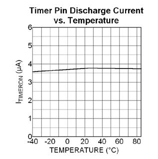
9 Typical Characteristics January 24, Revision 2.0


10 Typical Characteristics (Continued) January 24, Revision 2.0
11 Functional Characteristics January 24, Revision 2.0
12 Functional Diagram Block Diagram January 24, Revision 2.0
13 Functional Description Hot Swap Insertion When circuit boards are inserted into systems carrying live supply voltages ("hot swapped"), high inrush currents often result due to the charging of bulk capacitance that resides across the circuit board's supply pins. These current spikes can cause the system's supply voltages to temporarily go out of regulation causing data loss or system lock-up. In more extreme cases, the transients occurring during a hot swap event may cause permanent damage to connectors or other on-board components. The was designed to address these issues by limiting the maximum current that is allowed to flow during hot swap events. This is achieved by implementing a constant-current control loop at turn-on. In addition to inrush current control, the MIC2587 and MIC2587R incorporate input voltage supervisory functions and user-programmable overcurrent protection, thereby providing robust protection for both the system and the circuit board. Input Supply Transient Suppression and Filtering The is guaranteed to withstand transient voltage spikes up to 100V. However, voltage spikes in excess of 100V may cause damage to the controller. In order to suppress transients caused by parasitic inductances, wide (and short) power traces should be utilized. Alternatively, heavier trace plating will help minimize inductive spikes that may arise during events that cause a large di/dt to occur (e.g., short circuit loads). External surge protection, such as a clamping diode, is also recommended as an added safeguard for device, and system protection. And lastly, a 0.1µF decoupling capacitor from the VCC pin to ground is recommended to assist in noise rejection. Place this filter capacitor as close as possible to the VCC pin of the controller. Start-Up Cycle When the power supply voltage to the is higher than the V UVH and the V ONH threshold voltages, a start cycle is initiated. When the controller is enabled, an internal 16µA current source (I GATEON ) is turned on and the GATE pin voltage rises from 0V with respect to ground at a rate equal to Equation 1: where C GATE is the total capacitance seen at the GATE output of the controller (external capacitor from GATE to ground plus C GS of the external MOSFET). The internal charge pump has sufficient output drive to fully enhance commonly available power MOSFETs for the lowest possible DC losses. The gate drive is guaranteed to be between 7.5V and 18V over the entire supply voltage operating range (10V to 80V), so 60V BV DSS and 30V BV DSS N-channel power MOSFETs with a maximum gatesource voltage of 20V can be used for +48V and +24V applications, respectively. However, due to the harsh electrical environments of most backplanes and other live power supplies, the use of 100V and 60V power MOSFETs, respectively, is recommended to withstand transient spikes caused by stray inductances. Additionally, an external Zener diode (18-V) connected from the source to the gate as shown in the typical applications circuit is also recommended. A good choice for an 18-V Zener diode in this application is the MMSZ5248B, available in a small SOD123 package. C4 is used to adjust the GATE voltage slew rate while R3 minimizes the potential for high-frequency parasitic oscillations from occurring in M1. However, note that resistance in this part of the circuit has a slight destabilizing effect upon the 's current regulation loop. Compensation resistor R4 is necessary for stabilization of the current regulation loop. The current through the power transistor during initial inrush is given by: I INRUSH = C LOAD I GATEON C GATE Eq. 2 The drain current of the MOSFET is monitored via an external current sense resistor to ensure that it never exceeds the programmed threshold, as described in the "Circuit Breaker Operation" section. A capacitor connected to the controller s TIMER pin sets the value of overcurrent detector delay, t FLT, which is the time for which an overcurrent event must last to signal a fault condition and to cause the output to latch-off. The controller is most often utilized in applications with large capacitive loads, so a properly chosen value of C TIMER prevents false-, or nuisance-, tripping at turn-on as well as providing immunity to noise spikes after the start-up cycle is complete. The procedure for selecting a value for C TIMER is given in the "Circuit Breaker Operation" section. dv GATE dt = I GATEON C GATE Eq. 1 January 24, Revision 2.0
14 Overcurrent Protection The MIC2587 and the MIC2587R use an external, lowvalue resistor in series with the drain of the external MOSFET to measure the current flowing into the load. The VCC connection (Pin 8) and the SENSE connection (Pin 7) are the (+) and ( ) inputs, respectively, of the device's internal current sensing circuits. Kelvin sense connections are strongly recommended for sensing the voltage across these pins. See the Applications Information section for further details. The nominal current limit is determined by Equation 3: VTRIP(TYP) I LIM = Eq. 3 R SENSE Programming the response time of the overcurrent detector helps to prevent nuisance tripping of the circuit breaker attributed to transient current surges (e.g., inrush current charging bulk load capacitance). The nominal overcurrent response time (t FLT ) is approximated by Figure 4: t FLT C = (ms) t FLT TIMER I V TIMERUP 20 TIMERH C TIMER (µf) Eq. 4 The typical overcurrent filter delay time for several standard value capacitors is listed in Table 1. where V TRIP(TYP) is the typical current-limit threshold specified in the datasheet and R SENSE is the value of the selected sense resistor. The controllers employ a constant-current regulation scheme while in current limit. The internal charge pump s output voltage, seen at the GATE pin, is adjusted so that the voltage across the external sense resistor is held equal to V TRIP while the capacitor connected to the TIMER pin is being charged. If the current-limit condition goes away before the TIMER pin voltage rises above the V TIMERH threshold, then steady-state operation resumes. To prevent excessive power dissipation in the external MOSFET under load current fault conditions, the FB pin voltage is used as an input to a circuit that lowers the current limit as a function of the FB pin voltage. When the load current increases to the point where the output voltage at the load approaches 0V (likewise, the s FB pin voltage also approaches 0V), the result is a proportionate decrease in the maximum current allowed into the load. The transfer characteristic of this foldback current limit subcircuit is shown in Figure 1. When V OUT = V FB = 0V, the foldback current-limiting circuit controls the s GATE drive to force a constant 12mV (typical) voltage drop across the external sense resistor. Circuit Breaker Operation The is equipped with an electronic circuit breaker that protects the external N-channel power MOSFET and other system components against largescale output current faults, both during initial card insertion or during steady-state operation. The current limit threshold is set via an external resistor, R SENSE, connected between the controller s VCC (Pin 8) and SENSE (Pin 7) pins. For the, a fault current timing circuit is set via an external capacitor C TIMER that determines the length of the time delay for which the controller remains in current limit before the circuit breaker is tripped. Table 1. Overcurrent Filter Delay Time for Several Standard Capacitor Values C TIMER (µf) t FLT (ms) Whenever the voltage across R SENSE exceeds the s circuit-breaker threshold voltage (47mV typical) during steady-state operation, the following two events occur: A constant-current regulation loop engages within 1µs after an overcurrent condition is detected by the input sense pins monitoring the voltage across R SENSE. An internal 65µA current source (I TIMERUP ) begins to charge C TIMER. If the excessive current persists such that the voltage across C TIMER crosses the V TIMERH threshold (1.313V, typically), the circuit breaker trips and the GATE pin is immediately pulled low by a 80mA (typical) internal current sink while the TIMER pin is discharged to ground by a 3.5µA current sink (I TIMERDN). An initial value for C TIMER is found by calculating the time it will take for the to completely charge the output capacitive load during startup. The turn-on delay time is derived from the expression, I = C (dv/dt): CLOAD VCC(MAX) tturn-on = Eq. 5 ILIMIT January 24, Revision 2.0
15 Using parametric values for the, an expression relating a worst-case design value for C TIMER, using the specification limits, to the circuit's turn-on delay time is: C TIMER(MIN) C TIMER(MIN) C TIMER(MIN) t I TURN ON TIMERH(MAX) = V TIMERH(MIN) = t TURN ON = t TURN ON 120μ V μf sec. Eq. 6 For example, in a system with a C LOAD = 1000µF, a maximum V CC = +72V, and a maximum load current on a nominal +48V buss of 1.65A, the initial steps for the circuit design are: Choose I LIMIT = I HOT_SWAP(nom) = 2A (1.65A + 20%) Select an R SENSE (Closest 1% standard value is 19.6mΩ) Using I CHARGE = I LIMIT = 2A, the application circuit turnon time is calculated using Equation 5: t ( 1000µF 72V) TURN -ON = = 2A 36ms Allowing for capacitor tolerances and a maximum 36ms turn-on time, an initial worst-case value for C TIMER is: A standard 3.3µF ±5% tolerance capacitor would be a good initial starting value for prototyping since this value would allow the controller to start up without nuisance tripping over the entire voltage range given in the example application. Auto-Retry Period For the MIC2587R, once the overcurrent timer times out and the circuit breaker trips, the TIMER pin begins to discharge. Once the timer pin voltage discharges below the V TIMERL threshold, the circuit breaker resets to initiate another start-up cycle. If the overcurrent fault condition is still present, then the auto-retry cycle will continue until either of the following occurs: a) the fault condition is removed, b) the input supply voltage power is removed/recycled, or c) the ON pin is toggled LOW then HIGH. The duty cycle of the auto-restart function is therefore fixed at 5% and the nominal period of the autorestart cycle is given by: ( C ) ( V V ) TIMER TIMERH t AUTO-RETRY = 20 ITIMERH (ms) t AUTO-RETRY = 250 CTIMER (µf) TIMERL Eq. 7 The auto-restart period for the example above where the worst-case C TIMER was calculated to be 3.3µF is: t AUTO-RETRY = 825ms The typical auto-restart period for several standard value capacitors is listed in Table 2. C TIMER(MIN) μf = 0.036s sec. = 3.3µF Table 2. Auto-Restart Period for Several Standard Capacitor Values C TIMER (µf) t AUTO-RETRY (ms) January 24, Revision 2.0
16 Input Undervoltage Lockout The have an internal undervoltage lockout circuit that inhibits operation of the controller s internal circuitry unless the power supply voltage is stable and within an acceptable tolerance. If the supply voltage to the controller with respect to ground is greater than the V UVH threshold voltage (8V typical), the controller s internal circuits are enabled and the controller is then ready for normal operation pending the state of the ON pin voltage. Once in steady-state operation, the controller s internal circuits remain active so long as the supply voltage with respect to ground is higher than the controller s internal V UVL threshold voltage (7.5V typical). Power-is-Good Output Signals For the MIC and MIC2587R-1, the power-good output signal (PWRGD) will be high impedance when the FB pin voltage is higher than the V FBH threshold and will pull-down to GND when the FB pin voltage is lower than the V FBL threshold. For the MIC and MIC2587R-2, the power-good output signal (/PWRGD) will pull down to GND when the FB pin voltage is higher than the V FBH threshold and will be high impedance when the FB pin voltage is lower than the V FBL threshold. Hence, the ( 1) parts have an Active-HIGH PWRGD signal and the ( 2) parts have an Active-LOW /PWRGD output. PWRGD (or /PWRGD) may be used as an enable signal for one or more following DC/DC converter modules or for other system uses as desired. When used as an enable signal, the time necessary for the PWRGD (or /PWRGD) signal to pull-up (when in high impedance state) will depend upon the (RC) load at the Power-is-Good pin. The Power-is-Good output pin is connected to an opendrain, N-channel transistor implemented with high-voltage structures. These transistors are capable of operating with pull-up resistors to supply voltages as high as 100V. January 24, Revision 2.0
17 Application Information External ON/OFF Control The have an ON pin input that is used to enable the controller to commence a start-up sequence upon card insertion or to disable controller operation upon card removal. In addition, the ON pin can be used to reset the s internal electronic circuit breaker in the event of a load current fault. To reset the electronic circuit breaker, the ON pin is toggled LOW then HIGH. The ON pin is internally connected to an analog comparator with 80mV of hysteresis. When the ON pin voltage falls below its internal V ONL threshold, the GATE pin is immediately pulled low. The GATE pin will be held low until the ON pin voltage is above its internal V ONH threshold. The external circuit's ON threshold voltage level is programmed using a resistor divider (R1 & R2) as shown in the "Typical Application circuit. The equations to set the trip points are shown below. For the example illustrated in Equation 8, the supply voltage needed to turn on the controller is set to +37V, a value commonly used in +48V Central Office power distribution applications. R1+ R2 VIN(ON) = VONH Eq. 8 R2 Given V ONH and R2, a value for R1 can be determined. A suggested value for R2 is that which will provide at least 100µA of current through the voltage divider chain at V CC = V ONH. This yields the following as a starting point: VONH(TYP) 1.313V R2 = = = 13.13kΩ 100μA 100μA The closest standard 1% value for R2 is 13kΩ. Now, solving for R1 yields: V IN(ON) 37V R1= R2 1 = 13kΩ 1 = kω VONH(TYP) 1.313V Output Voltage Power-is-Good Detection The includes an analog comparator used to monitor the output voltage of the controller through an external resistor divider as shown in the Typical Application circuit. The FB input pin is connected to the non-inverting input and is compared against an internal reference voltage. The analog comparator exhibits a hysteresis of 80mV. Setting the Power-is-Good threshold for the circuit follows a similar approach as setting the circuit s ON/OFF input voltage. The equations to set the trip points are shown below. For the +48V telecom application shown in Equation 9, power-is-good output signal PWRGD (or /PWRGD) is to be de-asserted when the output supply voltage is lower than +48V-10% (+43.2V): R5 + R6 VOUT(NOT GOOD) = VFBL Eq. 9 R6 Given V FBL and R6, a value for R5 can be determined. A suggested value for R6 is that which will provide approximately 100µA of current through the voltage divider chain at V OUT(NOT GOOD) = V FBL. This yields the following equation as a starting point: VFBL(TYP) 1.233V R6 = = = kω Eq μ0 100μ0 The closest standard 1% value for R6 is 12.4kΩ. Now, solving for R5 yields: V OUT(NOT GOOD) 43.2V R5 = R6 1 = 12.4kΩ 1 = 422 kω VFBL(TYP) 1.233V The closest standard 1% value for R5 is 422kΩ. Using standard 1% resistor values, the external circuit's nominal power-is-good and power-is-not-good output voltages are V OUT(GOOD) = +46V and V OUT(NOT GOOD) = +43.2V. In solving for V OUT(GOOD), substitute V FBH for V FBL in Equation 9. The closest standard 1% value for R1 is 357kΩ. Using standard 1% resistor values, the external circuit's nominal ON and OFF thresholds are V IN(ON) = +36V and V IN(OFF) = +34V. In solving for V IN(OFF), replace V ONH with V ONL in Equation 8. January 24, Revision 2.0
18 Sense Resistor Selection The sense resistor is nominally valued at: where: VTRIP(TYP) R SENSE(NOM) = Eq. 11 I HOT_SWAP(NOM) V TRIP(TYP) is the typical (or nominal) circuit breaker threshold voltage (47mV) and I HOT_SWAP(NOM) is the nominal inrush load current level to trip the internal circuit breaker. To accommodate worst-case tolerances in the sense resistor (for a ±1% initial tolerance, allow ±3% tolerance for variations over time and temperature) and circuit breaker threshold voltages, a slightly more detailed calculation must be used to determine the minimum and maximum hot swap load currents. As the 's minimum current-limit threshold voltage is 39mV, the minimum hot swap load current is determined where the sense resistor is 3% high: 39mV I HOT_SWAP(MIN) = = 37.9mV ( 1.03 RSENSE(NOM) ) RSENSE(NOM) Keep in mind that the minimum hot swap load current should be greater than the application circuit's upper steady-state load current boundary. Once the lower value of R SENSE has been calculated, it is good practice to check the maximum hot swap load current (I HOT_SWAP(MAX) ) which the circuit may let pass in the case of tolerance build-up in the opposite direction. Here, the worst-case maximum is found using a V TRIP(MAX) threshold of 55mV and a sense resistor 3% low in value: In this case, the application circuit must be sturdy enough to operate over a ~1.5-to-1 range in hot swap load currents. For example, if an MIC2587 circuit must pass a minimum hot swap load current of 4A without nuisance trips, R SENSE should be set to: R SENSE(NOM) 39mV = = 9.75mΩ 4A where the nearest 1% standard value is 9.76mΩ. At the other tolerance extremes, I HOT_SWAP(MAX) for the circuit in question is then simply: I 56.7mV = 9.76mΩ HOT_SWAP(M AX) = 5.8A With a knowledge of the application circuit's maximum hot swap load current, the power dissipation rating of the sense resistor can be determined using P = I 2 R. Here, The current is I HOT_SWAP(MAX) = 5.8A and the resistance R SENSE(MIN) = (0.97)(R SENSE(NOM) ) = 9.47mΩ. Thus, the sense resistor's maximum power dissipation is: P MAX = (5.8A) 2 (9.47mΩ) = 0.319W A 0.5W sense resistor is a good choice in this application. When the s foldback current limiting circuit is engaged in the above example, the current limit would nominally fold back to 1.23A when the output is shorted to ground. 55mV I = = HOT_SWAP(MAX) 56.7mV R ( 0.97 RSENSE(NOM) ) SENSE(NOM) January 24, Revision 2.0

19 PCB Layout Recommendations 4-Wire Kelvin Sensing Because of the low value typically required for the sense resistor, special care must be used to accurately measure the voltage drop across it. Specifically, the measurement technique across R SENSE must employ 4- wire Kelvin sensing. This is simply a means of ensuring that any voltage drops in the power traces connected to the resistors are not picked up by the signal conductors measuring the voltages across the sense resistors. Figure 6 illustrates how to implement 4-wire Kelvin sensing. As the figure shows, all the high current in the circuit (from V CC through R SENSE and then to the drain of the N-channel power MOSFET) flows directly through the power PCB traces and through R SENSE. Other Layout Considerations Figure 8 is a recommended PCB layout diagram for the MIC2587-2YM. Many hot swap applications will require load currents of several amperes. Therefore, the power (V CC and Return) trace widths (W) need to be wide enough to allow the current to flow while the rise in temperature for a given copper plate (e.g., 1oz. or 2oz.) is kept to a maximum of 10 C to 25 C. Also, these traces should be as short as possible in order to minimize the IR drops between the input and the load. The feedback network resistor values in Figure 8 are selected for a +24V application. The resistors for the feedback (FB) and ON pin networks should be placed close to the controller and the associated traces should be as short as possible to improve the circuit s noise immunity. The input clamping diode (D1) is referenced in the Typical Application Circuit on Page 1. If possible, use highfrequency PCB layout techniques around the GATE circuitry (shown in the typical application circuit) and use a dummy resistor (e.g., R3 = 0Ω) during the prototype phase. If R3 is needed to eliminate high-frequency oscillations, common values for R3 range between 4.7Ω to 20Ω for various power MOSFETs. Finally, the use of plated-through vias will be needed to make circuit connection to the power and ground planes when utilizing multi-layer PCBs. Figure 6. 4-Wire Kelvin Sense Connections for R SENSE The voltage drop across R SENSE is sampled in such a way that the high currents through the power traces will not introduce significant parasitic voltage drops in the sense leads. It is recommended to connect the hot swap controller's sense leads directly to the sense resistor's metalized contact pads. The Kelvin sense signal traces should be symmetrical with equal length and width, kept as short as possible and isolated from any noisy signals and planes. In most applications, the use of a capacitor from the TIMER pin to ground will effectively eliminate nuisance tripping due to noise and/or transient overcurrent spikes. If the circuit breaker trips regularly due to a system environment that is vulnerable to noise being injected onto the Kelvin sense connections, the example circuit shown in Figure 7 can be implemented to combat such noisy environments. This circuit implements a 1.6 MHz low-pass filter to attenuate higher frequency disturbances on the current sensing circuitry. However, individual system analysis should be used to determine if filtering is necessary and to select the appropriate cutoff frequency for each specific application. Figure 7. Current-Limit Sense Filter for Noisy Systems January 24, Revision 2.0

20 Figure 8. Recommended PCB Layout for Sense Resistor, Power MOSFET, Timer and Feedback Network January 24, Revision 2.0
21 MOSFET and Sense Resistor Vendors Device types, part numbers, and manufacturer contacts for power MOSFETs and sense resistors are provided in Tables 3 and 4. Table 3. MOSFET Vendors MOSFET Vendors Key MOSFET Type(s) Breakdown Voltage (V DSS) Contact Information Vishay - Siliconix International Rectifier Renesas SUM75N06-09L (TO-263) SUM70N06-11 (TO-263) SUM50N06-16L (TO-263) SUP85N10-10 (TO-220AB) SUB85N10-10 (TO-263) SUM110N10-09 (TO-263) SUM60N10-17 (TO-263) IRF530 (TO-220AB) IRF540N (TO-220AB) 2SK1298 (TO-3PFM) 2SK1302 (TO-220AB) 2SK1304 (TO-3P) 60V 60V 60V 100V 100V 100V 100V 100V 100V 60V 100V 100V (203) (203) (310) (408) Table 4. Resistor Vendors Resistor Vendors Sense Resistors Contact Information Vishay - Dale WSL and WSR Series January 24, Revision 2.0
22 Package Information (1) 8-Pin SOIC (M) Note: 1. Package information is correct as of the publication date. For updates and most current information, go to MICREL, INC FORTUNE DRIVE SAN JOSE, CA USA TEL +1 (408) FAX +1 (408) WEB Micrel makes no representations or warranties with respect to the accuracy or completeness of the information furnished in this data sheet. This information is not intended as a warranty and Micrel does not assume responsibility for its use. Micrel reserves the right to change circuitry, specifications and descriptions at any time without notice. No license, whether express, implied, arising by estoppel or otherwise, to any intellectual property rights is granted by this document. Except as provided in Micrel s terms and conditions of sale for such products, Micrel assumes no liability whatsoever, and Micrel disclaims any express or implied warranty relating to the sale and/or use of Micrel products including liability or warranties relating to fitness for a particular purpose, merchantability, or infringement of any patent, copyright or other intellectual property right. Micrel Products are not designed or authorized for use as components in life support appliances, devices or systems where malfunction of a product can reasonably be expected to result in personal injury. Life support devices or systems are devices or systems that (a) are intended for surgical implant into the body or (b) support or sustain life, and whose failure to perform can be reasonably expected to result in a significant injury to the user. A Purchaser s use or sale of Micrel Products for use in life support appliances, devices or systems is a Purchaser s own risk and Purchaser agrees to fully indemnify Micrel for any damages resulting from such use or sale Micrel, Incorporated. January 24, Revision 2.0
MIC2587 Evaluation Board
 MIC2587 Evaluation Board Single Channel, Positive Voltage Hot Swap Controller General Description MIC2587/MIC2587R Hot Swap Controller The MIC2587 is a single-channel, positive voltage hot swap controller
MIC2544A/2548A. General Description. Features. Applications. Typical Application. Programmable Current Limit High-Side Switch
 Programmable Current Limit High-Side Switch General Description The MIC2544A and MIC2548A are integrated, high-side power switches optimized for low loss DC power switching and other power management applications,
Features. V CC 2.7V to 5.5V 10k OVERCURRENT GND NC
 MIC225/275 MIC225/275 Single-Channel Power Distribution Switch MM8 General Description The MIC225 and MIC275 are high-side MOSFET switches optimized for general-purpose power distribution requiring circuit
MIC2027/2077. Features. General Description. Applications. Typical Application. Quad USB Power Distribution Switch
 Quad USB Power Distribution Switch General Description The MIC2027 and MIC2077 are quad high-side MOSFET switches optimized for general-purpose power distribution requiring circuit protection. The MIC2027/77
MIC2546/2547. Features. General Description. Applications. Typical Application. Dual Programable Current Limit Switch
 Dual Programable Current Limit Switch General Description The MIC2546 and MIC2547 are integrated high-side dual power switches optimized for low loss dc power switching and other power management applications,
MIC1832. General Description. Features. Applications. Typical Application
 3.3V Voltage Supervisor with Manual Reset, Watchdog Timer and Dual Reset Outputs General Description The is a low-current microprocessor supervisor for monitoring 3.3V and 3V systems. The device features
TYPICAL APPLICATIO. LT1641-1/LT Positive High Voltage Hot Swap Controllers DESCRIPTIO FEATURES APPLICATIO S
 Positive High Voltage Hot Swap Controllers FEATURES Allows Safe Board Insertion and Removal from a Live Backplane Controls Supply Voltage from 9V to 0V Programmable Analog Foldback Current Limiting High
Features VDDA OUT1 ILIMIT CGATE1 FAULT#1 FAULT#2 ON1 ON2 MIC2596 OUT2 VDDL CGATE2 CTIMER1 CTIMER2 ILIMIT2 COL1 C5 COL2 VEE. System-Controlled Hot Swap
 MIC2596/2597 Dual Channel Negative Voltage Hot Swap Controllers Final Information General Description The MIC2596 and MIC2597 are dual channel negative voltage hot swap controllers designed to facilitate
MIC826. General Description. Features. Applications. Typical Application
 Voltage Supervisor with Watchdog Timer, Manual Reset, and Dual Outputs In 1.6mm x 1.6mm TDFN General Description The is a low-current, ultra-small, voltage supervisor with manual reset input, watchdog
Features VCC MIC1810 RESET RESET
 Microprocessor Reset Circuit General Description The is an inexpensive microprocessor supervisory circuit that monitors power supplies in microprocessor based systems. The function of these devices is
DESCRIPTIO FEATURES APPLICATIO S. LT1641 Positive High Voltage Hot Swap Controller TYPICAL APPLICATIO
 FEATURES Allows Safe Board Insertion and Removal from a Live Backplane Controls Supply Voltage from 9V to 0V Programmable Analog Foldback Current Limiting High Side Drive for an External N-Channel Automatic
Features. 10k. 10k ON/OFF. 1µF OVERCURRENT OVERCURRENT. Typical Two-Port Bus-Powered Hub
 MIC2536 Dual USB Power Distribution Switch Final Information General Description The MIC2536 is a cost-effective high-side power switch, with two independently controlled channels, optimized for buspowered
MIC2026A/2076A. General Description. Features. Applications. Typical Application. Dual-Channel Power Distribution Switch
 MIC226A/276A Dual-Channel Power Distribution Switch General Description The MIC226A and MIC276A are high-side MOSFET switches optimized for general-purpose power distribution requiring circuit protection.
MIC5281. Features. General Description. Applications. Typical Application. 120V IN, 25mA, Ultra-Low IQ, High-PSRR Linear Regulator
 120V IN, 25mA, Ultra-Low IQ, High-PSRR Linear Regulator General Description The high-performance linear regulator offers a very-wide input operating voltage range, up to 120V DC, and supplies an output
Features. Applications
 Micro-Power Voltage Supervisor IttyBitty General Description The is a power supply supervisor that provides undervoltage monitoring, manual reset capability, and power-on reset generation in a compact
MIC706P/R/S/T, MIC708R/S/T
 MIC706P/R/S/T, MIC708R/S/T µp Supervisory Circuit General Description The MIC706 and MIC708 are inexpensive microprocessor supervisory circuits that monitor power supplies in 3.0 and 3.3 microprocessor-based
MIC705/706/707/708. General Description. Features. Applications. Typical Application. µp Supervisory Circuit
 µp Supervisory Circuit General Description The MIC705, MIC706, MIC707, and MIC708 are inexpensive microprocessor supervisory circuits that monitor power supplies in microprocessor-based systems. The circuit
MIC2790/1/3. General Description. Features. Applications. Typical Application
 Supervisor with High-Accuracy, Ultra-Fast Propagation Delay, and Capacitor-Programmable Reset Delay General Description The is ideal for monitoring highly-accurate core voltages that require rapid response
SY89645L. General Description. Features. Block Diagram. Applications. Markets. Precision Low Skew, 1-to-4 LVCMOS/LVTTL-to-LVDS Fanout Buffer
 Precision Low Skew, 1-to-4 LVCMOS/LVTTL-to-LVDS Fanout Buffer General Description The is a 3.3V, fully differential, low skew, 1:4 LVDS fanout buffer that accepts LVTTL or LVCMOS inputs. It is capable
MIC2790/1/3. General Description. Features. Applications. Typical Application
 Supervisor with High-Accuracy, Ultra-Fast Propagation Delay, and Capacitor-Programmable Reset Delay General Description The is ideal for monitoring highly-accurate core voltages that require rapid response
Features. LOAD SWITCH or PMIC. LOAD SWITCH or PMIC /RESET
 Dual-Input Push Button Reset IC with Immediate and Delayed Outputs General Description The is a two input, two output push-button reset IC. It will generate a reset pulse for a factory-programmed reset
MIC2782. General Description. Features. Applications. Typical Application. Dual-Input Push Button Reset IC with Immediate and Delayed Outputs
 Dual-Input Push Button Reset IC with Immediate and Delayed Outputs General Description The is a two input, two output push button reset IC. It will generate a reset pulse for a factory programmed reset
Features. Applications
 Push-Button Reset IC General Description The are low-current, ultra-small, pushbutton reset supervisors with long set-up delays. The devices feature two manual reset inputs and two reset outputs. The devices
MIC2560. General Description. Features. Applications. Typical Application. PCMCIA Card Socket V CC and V PP Switching Matrix
 PCMCIA Card Socket V CC and V PP Switching Matrix General Description The V CC and V PP Matrix controls PCMCIA (Personal Computer Memory Card International Association) memory card power supply pins, both
MIC5282. General Description. Features. Applications. Typical Applications. 120V IN, 50mA, Ultra-Low I Q, High-PSRR Linear Regulator
 12V IN, 5mA, Ultra-Low I Q, High-PSRR Linear Regulator General Description The high-performance linear regulator offers a very-wide input operating voltage range, up to 12V DC, and supplies an output current
Features. Applications. Micrel Inc Fortune Drive San Jose, CA USA tel +1 (408) fax + 1 (408)
 fax + 1 (408)") Microprocessor Reset Circuits General Description The MIC809 and MIC810 are inexpensive microprocessor supervisory circuits that monitor power supplies in microprocessor-based systems. The function of
Microprocessor Reset Circuits General Description The MIC809 and MIC810 are inexpensive microprocessor supervisory circuits that monitor power supplies in microprocessor-based systems. The function of
Features. Applications. MIC4126/27/28 Block Diagram
 Dual 1.5A-Peak Low-Side MOSFET Drivers in Advanced Packaging General Description The MIC4126, MIC4127, and MIC4128 family are highlyreliable dual 1.5A low-side MOSFET drivers fabricated on Micrel s BiCMOS/DMOS
MIC2039. General Description. Features. Applications. Typical Application. High-Accuracy, High-Side, Adjustable Current Limit Power Switch
 MIC239 High-Accuracy, High-Side, Adjustable Current Limit Power Switch General Description The MIC239 is a high-side MOSFET power distribution switch providing increased system reliability by using 5%
Features. Applications. Regulator with Adjustable Output
 Low-Quiescent Current 150mA LDO Regulator General Description The is a low-quiescent current, μcap lowdropout regulator. With a maximum operating input voltage of 30V and quiescent current of 20μA, it
Features. Applications
 Push-Button Reset IC with Voltage Supervisor General Description The are low-current, ultra-small, pushbutton supervisor reset ICs with an integrated supply voltage monitor. The device features two manual
Features. Applications
 HCSL-Compatible Clock Generator for PCI Express General Description The is the smallest, high performance, lowest power, 2 differential output clock IC available for HCSL timing applications. offers -130dBc
Features MIC2779L IN OUT HTH GND. Cellular Telephone Battery Monitor
 MIC2779 Voltage Monitor with Adjustable Hysteresis General Description The MIC2779 is a voltage monitor uniquely designed to detect two separate voltage thresholds combined with a delay generator and logic.
MIC24051 Evaluation Board
 6A, High-Efficiency, Synchronous DC/DC Buck Regulator with Hyper Speed Control SuperSwitcher II General Description The MIC2451 DC/DC synchronous buck regulator operates over an input supply range of 4.5V
Features. Applications
 Ultra-Precision 1:8 CML Fanout Buffer with Internal I/O Termination General Description The is a 2.5V/3.3V precision, high-speed, fully differential CML 1:8 fanout buffer. The is optimized to provide eight
V PP IN V CC3 IN V CC5 IN EN0 EN1 MIC2561 V CC5_EN V CC3_EN
 MIC2561 PCMCIA Card Socket and V PP Switching Matrix Final Information General Description The MIC2561 & V PP Matrix controls PCMCIA (Personal Computer Memory Card International Association) memory card
LM3526 Dual Port USB Power Switch and Over-Current Protection
 LM3526 Dual Port USB Power Switch and Over-Current Protection General Description The LM3526 provides Universal Serial Bus standard power switch and over-current protection for all host port applications.
MAQ5281. Features. General Description. Applications. Typical Applications. 120V IN, 25mA, Ultra-Low I Q, High-PSRR Linear Regulator Automotive
 120V IN, 25mA, Ultra-Low I Q, High-PSRR Linear Regulator Automotive General Description The high-performance linear regulator offers a very-wide input operating voltage range, up to 120V DC, and supplies
Features. Applications
 2.5/3.3V 1-to-1 Differential to LVCMOS/LVTTL Translator Precision Edge General Description Micrel s is a 1-to-1, differential-to-lvcmos / LVTTL translator. The differential input is highly flexible and
 Distributed by: www.jameco.com 1-800-831-4242 The content and copyrights of the attached material are the property of its owner. LM3525 Single Port USB Power Switch and Over-Current Protection General
MP5013A 5 V, 5 A Programmable Current-Limit Switch with Over-Voltage Clamp and Slew-Rate Control in TSOT23-8
 The Future of Analog IC Technology MP5013A 5 V, 5 A Programmable Current-Limit Switch with Over-Voltage Clamp and Slew-Rate Control in TSOT23-8 DESCRIPTION The MP5013A is a protection device designed to
ZSPM4121. Under-Voltage Load Switch for Smart Battery Management. Datasheet. Brief Description. Features. Related IDT Smart Power Products
 Under-Voltage Load Switch for Smart Battery Management ZSPM4121 Datasheet Brief Description The ZSPM4121 battery management load switch can be used to protect a battery from excessive discharge. It actively
MAQ5282. Features. General Description. Applications. Typical Applications. 120V IN, 50mA, Ultra-Low I Q, High-PSRR Linear Regulator Automotive
 12V IN, 5mA, Ultra-Low I Q, High-PSRR Linear Regulator Automotive General Description The high-performance linear regulator offers a very-wide input operating voltage range, up to 12V DC, and supplies
Features. Slot A Address and data lines between logic controller and PCMCIA cards not shown. System Power Supply 12V 3.3V V CC5 IN A V PP OUT
 MIC2564A Dual Serial PCMCIA/CardBus Power Controller General Description The MIC2564A is dual-slot PC Card PCMCIA (Personal Computer Memory Card International Association) and CardBus power controller.
Features. Applications
 3.3V Ultra-Precision 1:4 LVDS Fanout Buffer/Translator with Internal Termination General Description The is a 3.3V, high-speed 2GHz differential low voltage differential swing (LVDS) 1:4 fanout buffer
Overvoltage-Protection Controllers with a Low RON Internal FET MAX4970/MAX4971/MAX4972
 19-4139; Rev 1; 8/08 Overvoltage-Protection Controllers General Description The family of overvoltage protection devices features a low 40mΩ (typ) R ON internal FET and protect low-voltage systems against
SM Features. General Description. Typical Application MHz/312.5MHz and MHz/156.25MHz LVDS Clock Synthesizer.
 156.25MHz/312.5MHz and 78.125MHz/156.25MHz LVDS Clock Synthesizer ClockWorks Flex General Description The is a member of the ClockWorks family of devices from Micrel and provides an extremely low-noise
STBC ma standalone linear Li-Ion battery charger with thermal regulation. Description. Features. Applications
 800 ma standalone linear Li-Ion battery charger with thermal regulation Description Datasheet - production data Features Programmable charge current up to 800 ma No external MOSFET, sense resistors or
Features. Applications
 6GHz, 1:4 CML Fanout Buffer/Translator with Internal I/O Termination General Description The is a 2.5V/3.3V precision, high-speed, fully differential 1:4 CML fanout buffer. Optimized to provide four identical
Features MIC2551A VBUS R S. 1.5k D+ D GND VM D SPD SUS GND. Typical Application Circuit
 MIC2551 USB Transceiver General Description The MIC2551 is a single chip transceiver that complies with the physical layer specifications of the Universal Serial Bus (USB) 2.0. It supports both full speed
SM General Description. Features. Block Diagram. ClockWorks TM 125MHz LVDS / 125 MHz HCSL Ultra-Low Jitter Frequency Synthesizer
 ClockWorks TM 125MHz LVDS / 125 MHz HCSL Ultra-Low Jitter Frequency Synthesizer General Description The is a member of the ClockWorks family of devices from Micrel and provides an extremely low-noise timing
AAT4625 PRODUCT DATASHEET. USB Single-Channel Power Switch. General Description. Features. Applications. Typical Application AAT4625 OUT
 General Description The SmartSwitch is part of AnalogicTech s Application Specific Power MOSFET (ASPM ) product family. It is a 1.0A current limited P-channel MOSFET power switch designed for high-side
MP5013E 5V, 2A, Programmable Current- Limit Switch with Over-Voltage Clamp and Slew Rate Control in a TSOT23-8
 MP5013E 5V, 2A, Programmable Current- Limit Switch with Over-Voltage Clamp and Slew Rate Control in a TSOT23-8 DESCRIPTION The MP5013E is a protection device designed to protect circuitry on the output
VCC 1 GND. Environmental. Pb-Free Halogen Free. V D = 20V Max* 5V 3.3V G1/G2 PG 8 DIS2 3
 Not for Distribution Features 5V Power supply Drain Voltage Range 1.0V to 20V Internal Gate Voltage Charge Pump Controlled Load Discharge Rate Controlled Turn on Slew Rate TDFN-8 Package Application Functions
STEF12E. Electronic fuse for 12 V line. Datasheet. Features. Applications. Description
 Datasheet Electronic fuse for 12 V line Features DFN10 (3x3 mm) Continuous current typ. 3.6 A N-channel on-resistance typ. 45 mω Enable/fault functions Output clamp voltage typ. 15 V Undervoltage lockout
+3.0V to +5.5V USB Power Control Switch
 SP55 +3.0V to +5.5V USB Power Control Switch Compliant to USB Specifications +3.0V to +5.5V Input Voltage Range Open Drain Error Flag Output.7V Undervoltage Lockout 500mA Minimum Continuous Load Current.5A
DESCRIPTIO APPLICATIO S TYPICAL APPLICATIO. LT1640AL/LT1640AH Negative Voltage Hot Swap Controller FEATURES
 LT60AL/LT60AH Negative oltage Hot Swap Controller FEATURES Allows Safe Board Insertion and Removal from a Live Backplane Operates from 0 to 0 Programmable Inrush Current Allows 50mA of Reverse Drain Pin
+60V Simple Swapper Hot-Swap Switch
 19-2850; Rev 0; 4/03 +6 Simple Swapper Hot-Swap Switch General Description The is a fully integrated Simple Swapper hot-swap switch for positive supply rails. The device allows the safe insertion and removal
High-side Power Distribution Switch NCT3521U
 High-side Power Distribution Switch NCT3521U -Table of Content- 1. GENERAL DESCRIPTION...1 2. FEATURES...1 3. APPLICATIONS...2 4. PIN CONFIGURATION AND DESCRIPTION...2 5. TYPICAL APPLICATION CIRCUIT...3
MIC29150/29300/29500/29750
 High-Current Low-Dropout Regulators General Description The are high current, high accuracy, low-dropout voltage regulators. Using Micrel's proprietary Super βeta PNP process with a PNP pass element, these
SM Features. General Description. Applications. Block Diagram
 ClockWorks Fibre Channel (106.25MHz, 212.5MHz) Ultra-Low Jitter, LVDS Frequency Synthesizer General Description The is a member of the ClockWorks family of devices from Micrel and provides an extremely
SP V to +5.5V USB Power Control Switch Compliant to USB Specifications +3.0V to +5.5V Input Voltage Range Open Drain Error Flag Output 2.7V Un
 SP55 +3.0V to +5.5V USB Power Control Switch Compliant to USB Specifications +3.0V to +5.5V Input Voltage Range Open Drain Error Flag Output.7V Undervoltage Lockout 500mA Minimum Continuous Load Current.5A
MP201 Dying Gasp Storage and Release Control IC
 The Future of Analog IC Technology MP201 Dying Gasp Storage and Release Control IC DESCRIPTION The MP201 is a dying gasp storage and release controller. It charges storage capacitor from the input during
AIC1520. Ferrite Bead GND. *33µF, 16V Tantalum, or 100µF, 10V Electrolytic Bold line indicate high-current traces. USB High-Side Power Switch
 USB High-Side Power Switch FEATURES 120mΩ (5V Input) High-Side MOSFET Switch. 500mA Continuous Load Current. 80µA Typical On-State Supply Current. Current-Limit / Short Circuit Protection. Thermal Limiting
MP6219 5V, 1A 2A Programmable Current Limit Power Distribution Switch
 The Future of Analog IC Technology MP6219 5V, 1A 2A Programmable Current Limit Power Distribution Switch DESCRIPTION The MP6219 is a protection device designed to protect circuitry on the output from transients
AIC A Dual USB High-Side Power Switch FEATURES DESCRIPTION APPLICATIONS TYPICAL APPLICATION CIRCUIT
 1.0A Dual USB High-Side Power Switch FEATURES 2.7V to 6.5V Input Voltage Range 1.0A Dual Continuous Load Current 100mΩ High-Side P-MOSFET Switch 20Ω Open-Drain Over-Current Flag Output 80uA Quiescent Supply
MP5007 5V, 1A- 5A Programmable Current Limit Switch
 The Future of Analog IC Technology DESCRIPTION The MP5007 is a protection device designed to protect circuitry on the output (source) from transients on input (V CC ). It also protects V CC from undesired
NOT RECOMMENDED FOR NEW DESIGN NO ALTERNATE PART. Applications
 3.6A 5V RESETTABLE ELECTRONIC FUSE Description Pin Assignments The is a self-protected resettable electronic fuse designed for consumer applications such as hard disk drives to industrial applications
MIC5159. General Description. Features. Applications. Typical Application. Programmable Current Limit µcap LDO Regulator Controller
 Programmable Current Limit µcap LDO Regulator Controller General Description Micrel s is a precision-voltage regulator controller. Used with an external P-Channel MOSFET, the forms a two-chip low-dropout
HF81 X Capacitor Bleeder
 HF81 X Capacitor Bleeder The Future of Analog IC Technology DESCRIPTION HF81 is an innovative two-terminal IC that automatically discharges an X capacitor while eliminating power losses and allowing power
Features. Description. Applications. Block Diagram PT7M3808. Fixed Voltage Diagram. Adjustable Voltage Diagram(PT7M3808G01)
") Features Description Power-On Reset Generator with Adjustable Delay Time: 1.25ms to 10s. Very Low Quiescent Current: 2.8µA Typical High Threshold Accuracy: 0.5% Typ. Fixed Threshold Voltages for Standard
Features Description Power-On Reset Generator with Adjustable Delay Time: 1.25ms to 10s. Very Low Quiescent Current: 2.8µA Typical High Threshold Accuracy: 0.5% Typ. Fixed Threshold Voltages for Standard
Micrel Inc Fortune Drive San Jose, CA USA tel +1 (408) fax + 1 (408)
 fax + 1 (408)") DSC2311KL2R008 Crystalless Configurable Clock Generator General Description DSC2311KL2R008 is a crystalless clock generator that is factory configurable to simultaneously output two separate frequencies
DSC2311KL2R008 Crystalless Configurable Clock Generator General Description DSC2311KL2R008 is a crystalless clock generator that is factory configurable to simultaneously output two separate frequencies
MAX14653/MAX14654/ MAX14655/MAX High-Current Overvoltage Protectors with Adjustable OVLO
 EVALUATION KIT AVAILABLE MAX14653/MAX14654/ General Description The MAX14653/MAX14654/ overvoltage protection devices feature a low 38mΩ (typ) R ON internal FET and protect low-voltage systems against
GreenFET TM High Voltage Gate Driver CC D Q-PUMP + _. Timing & Logic. Discharge
 GreenFET TM High Voltage Gate Driver Features 5V ±5% Power supply SLG55021 Drain Voltage Range 1.0V to 20V Internal Gate Voltage Charge Pump Controlled Turn on Delay Controlled Load Discharge Rate Controlled
SY55854U. General Description. Features. Functional Block Diagram. Applications. 2 x 2 Protection Crosspoint Switch
 2 x 2 Protection Crosspoint Switch General Description The is a fully differential, CML, 2 x 2-crosspoint switch. The non-blocking design allows any input to be connected to any output. Varying the state
PI5USB2549 USB Charging Port Controller and Load Detection Power Switch
 Features Supports DCP Modes per USB Battery Charging Specification 1.2 Supports Shorted Mode per Chinese Telecommunication Industry Standard YD/T1591-2009 Supports non-bc1.2 Charging Modes by Automatic
AN3050 Application note
 Application note STBP120 overvoltage protection device 1 Introduction In order to reduce the power consumption, size and cost of electronic devices, most semiconductor components are manufactured using
Environmental G1/G2. Timing & Logic. Discharge S/DIS1. The highest V D being switched must be at FET1 and pin 5 of the SLG55221 and SLG55220
 2 Rail GreenFET TM High Voltage Gate Driver Features 5V Power supply Drain Voltage Range 1.0V to 6V Internal Gate Voltage Charge Pump Controlled Load Discharge Rate Controlled Turn on Slew Rate TDFN-8
Control Circuitry 2 M1. Micrel Inc Fortune Drive San Jose, CA USA tel +1 (408) fax + 1 (408)
 fax + 1 (408)") Crystal-less Configurable Clock Generator General Description The is a programmable, high performance dual LVDS output oscillator utilizing Micrel's proven silicon MEMS technology to provide excellent
Crystal-less Configurable Clock Generator General Description The is a programmable, high performance dual LVDS output oscillator utilizing Micrel's proven silicon MEMS technology to provide excellent
AN2408 Application note
 Application note 900mA standalone linear Li-Ion battery charger with thermal regulation Introduction One way to minimize the size and complexity of a battery charger is to use a linear-type charger. The
3.3V, 2.0GHz ANY DIFF. IN-TO-LVDS PROGRAMMABLE CLOCK DIVIDER FANOUT BUFFER W/ INTERNAL TERMINATION
 3.3V, 2.0GHz ANY DIFF. -TO-LVDS PROGRAMMABLE CLOCK DIVIDER FANOUT BUFFER W/ TERNAL TERMATION FEATURES Guaranteed AC performance > 2.0GHz f MAX output toggle > 3.0GHz f MAX input < 800ps t PD (matched-delay
Features. (opt) A EN0 A EN1 A V CC5_EN A V CC3_EN MIC2563 B EN0 B EN1 B V CC5_EN B V CC3_EN
 A EN0 A EN1 A V CC5_EN A V CC3_EN MIC2563 B EN0 B EN1 B V CC5_EN B V CC3_EN") MIC2563A ual-slot /CardBus Power Controller General escription The MIC2563A dual-slot (Personal Computer Memory Card International Association) and CardBus power controller handles all PC Card slot power
MIC2563A ual-slot /CardBus Power Controller General escription The MIC2563A dual-slot (Personal Computer Memory Card International Association) and CardBus power controller handles all PC Card slot power
AIC1526. Dual USB High-Side Power Switch FEATURES DESCRIPTION APPLICATIONS
 Dual USB High-Side Power Switch FEATURES 110mΩ (5V Input) High-Side MOSFET Switch. 500mA Continuous Load Current per Channel. 110µA Typical On-State Supply Current. 1µA Typical Off-State Supply Current.
up7535 Dual-Input Triple-Output Power Multiplexer in PSOP-8L for USB High Side Switch General Description Ordering Information Applications
 Dual-Input Triple-Output Power Multiplexer in PSOP-8L for USB High Side Switch The up7535 is a current limited, dual-input triple-output power multiplexer acting as a high side switch for USB applications
PART TOP VIEW. TO LOAD SINGLE Li+ CELL TO IN LOGIC OUT. Maxim Integrated Products 1
 19-224; Rev 2; 6/3 USB-Powered Li+ Charger General Description The is a single-cell lithium-ion (Li+) battery charger that can be powered directly from a USB port* or from an external supply up to 6.5V.
DSC2033. Low-Jitter Configurable Dual LVDS Oscillator. General Description. Features. Block Diagram. Applications
 General Description The series of high performance dual output LVDS oscillators utilize a proven silicon MEMS technology to provide excellent jitter and stability while incorporating additional device
AOZ8101. Ultra-Low Capacitance TVS Diode Array. General Description. Features. Applications. Typical Application
 Ultra-Low Capacitance TS Diode Array General Description The AOZ8101 is a transient voltage suppressor array designed to protect high speed data lines from Electro Static Discharge (ESD) and lightning.
STEF01. 8 V to 48 V fully programmable universal electronic fuse. Description. Features. Applications
 8 V to 48 V fully programmable universal electronic fuse Datasheet - production data Features Operating input voltage range: 8 to 48 V Absolute maximum input voltage: 55 V Continuous current typ.: 4 A
HM9708 HM9708. Battery-Powered Equipment Motherboard USB Power Switch USB Device Power Switch Hot-Plug Power Supplies Battery-Charger Circuits DC+ VIN
 200mΩ Power Distribution Switches Features 200mΩ Typ. High-Side MOSFET 0.8A Current Limit (V IN =3.0V) Wide Input Voltage Range: 2V ~ 5.5V Soft Start Thermal Protection Small SOT-23-5 Package Minimizes
STBC mA Standalone linear Li-Ion Battery charger with thermal regulation. Feature summary. Description. Applications.
 800mA Standalone linear Li-Ion Battery charger with thermal regulation Feature summary Programmable charge current up to 800mA No external MOSFET, sense resistors or blocking diode required Complete linear
EVALUATION KIT AVAILABLE 28V Linear Li+ Battery Charger with Smart Autoboot Assistant OFF
 19-994; Rev 2; 3/8 EVALUATION KIT AVAILABLE 28V Linear Li+ Battery Charger with General Description The intelligent, stand-alone constant-current, constant-voltage (CCCV), thermally regulated linear charger
APPLICATIO S. LTC1646 CompactPCI Dual Hot Swap Controller DESCRIPTIO FEATURES TYPICAL APPLICATIO
 FEATURES Allows Safe Board Insertion and Removal from a Live, CompactPCI TM Bus Controls 3.3V and/or Supplies Programmable Foldback Current Limit During Power-Up Dual Level Circuit Breakers Protect Supplies
2. Control Pin Functions and Applications
 IMARY CONTROL ( PIN) Module Enable / Disable. The module can be disabled by pulling the below 2.3 V with respect to the Input. This should be done with an open-collector transistor, relay, or optocoupler.
ZLED7002. Toggle (Side-Step) Dual-Channel LED Driver. Datasheet. Features. Brief Description. Benefits. Available Support. Physical Characteristics
 Dual-Channel LED Driver. Datasheet. Features. Brief Description. Benefits. Available Support. Physical Characteristics") Toggle (Side-Step) Dual-Channel LED Driver ZLED7002 Datasheet Brief Description The ZLED7002 toggle (side-step) dual-channel LED driver is one of our ZLED family of LED control ICs. It operates in the
Toggle (Side-Step) Dual-Channel LED Driver ZLED7002 Datasheet Brief Description The ZLED7002 toggle (side-step) dual-channel LED driver is one of our ZLED family of LED control ICs. It operates in the
Craft Port Tiny RS-232 Transceiver for Portable Applications ADM101E. Data Sheet FUNCTIONAL BLOCK DIAGRAM
 Data Sheet FEATURES 460 kbit/s Transmission Rate Single 5 V Power Supply Compatible with RS-232 Input/Output Levels 0.1 μf Charge Pump Capacitors One Driver and One Receiver On-Board DC-DC Converter ±4.2
GENERAL DESCRIPTION APPLICATIONS FEATURES TYPICAL APPLICATION DIAGRAM
 August 2009 Rev. 2.0.0 GENERAL DESCRIPTION The SP6686 is a current-regulated charge pump ideal for powering high brightness LEDs for camera flash applications. The charge pump can be set to regulate two
APX803/D 3-PIN MICROPROCESSOR RESET CIRCUIT. Description. Pin Assignments. Features. Applications APX803. ( Top View ) SOT23. ( Top View ) SOT23R GND
 SOT23. ( Top View ) SOT23R GND") /D Description Pin Assignments The /D is used for microprocessor (µp) supervisory circuits to monitor the power supplies in µp and digital ( Top View ) systems. They provide excellent circuit reliability
/D Description Pin Assignments The /D is used for microprocessor (µp) supervisory circuits to monitor the power supplies in µp and digital ( Top View ) systems. They provide excellent circuit reliability
AMD Athlon. Processor. Voltage Regulation Design. Application Note. Publication # Rev: E-1 Issue Date: February 2000
 AMD Athlon TM Processor Voltage Regulation Design Application Note Publication # 22651 Rev: E-1 Issue Date: February 2000 2000 Advanced Micro Devices, Inc. All rights reserved. The contents of this document
2:1 MULTIPLEXER CHIP FOR PCI-EXPRESS ICS Description. Features. Block Diagram DATASHEET
 DATASHEET 2:1 MULTIPLEXER CHIP FOR PCI-EXPRESS ICS557-08 Description The ICS557-08 is a 2:1 multiplexer chip that allows the user to select one of the two HCSL (Host Clock Signal Level) or LVDS input pairs
MIC A Evaluation Board
 75V/4A Hyper Speed Control Synchronous DC/DC Buck Regulator General Description meter and V IN at Vin and GND terminals with voltmeter. Do not apply power until Step 5. The MIC28500 DC/DC regulator operates
VRM 8.1 DC-DC Converter Design Guidelines
 VRM 8.1 DC-DC Converter Design Guidelines May 1997 Order Number: 243408-001 Information in this document is provided in connection with Intel products. No license, express or implied, by estoppel or otherwise,