Published on Online Documentation for Altium Products (
|
|
|
- Griffin Terry
- 5 years ago
- Views:
Transcription
1 Published on Online Documentation for Altium Products ( Home > Support for Parameters in PCB Footprints Using Altium Documentation Modified by Jason Howie on Apr 11, 2017 Parameters applied to objects in Altium Designer provide a powerful and flexible means of adding additional information to a PCB design. Applied as properties of the parent object, Parameters can be applied at a range of levels, including to projects, documents, templates and individual objects within a design document. See the Parameter Object reference for more information Along with a range of standard, predefined parameters (special strings) from the document name (DocumentName) through a component s footprint model (CurrentFootprint) Altium Designer also offers the capability of defining custom User Parameters. To date, these have been available at the Project, Document and Schematic sheet level, but not explicitly in the PCB footprint space. Altium Designer 17 introduces that capability, and in a way that functions in concert with parameters defined at the core schematic level and therefore retaining a unified Schematic PCB relationship. Parameters that become available in the PCB space can be used for filter Queries, Design Rules, Scripts and Variants, and applied in PCB component Libraries for invoking custom strings in placed Footprints. Parameters via an Engineering Change Order The new PCB parameter capabilities are based on additional functionality included in the ECO mechanism and PCB document, which allow user defined component parameters to be transferred to and retained in the PCB space. This is a one-way transfer, and the passed parameters are read-only in the PCB domain. The parameter transfer is performed by simply instigating an ECO from the Schematic to PCB with the Design» Update PCB Document menu command.

2 Updating the PCB via the ECO dialog detects and transfers User Defined schematic component parameters to the corresponding PCB footprints. When the ECO is executed, any new user defined schematic component Parameters will be transferred to the corresponding footprint reference in the PCB design. In the above example image, the Design Item Id parameter attached to all schematic components is detected and assigned as a sequence of ECO updates to the PCB. The detection and migration of parameters to the PCB is determined by the project's option settings (Project» Project Options). In the Options dialog, use the Parameters section under the Comparator and ECO Generation tabs to set the difference detection and modification behavior. To observe the transferred parameters in the PCB editor, open the properties of a component and click the button in the dialog. The following Parameters dialog will list the current user parameters that have been assigned to the selected component footprint.

3 As you would expect, parameters for a selected component footprint are also available in the PCB Inspector panel.
 that normally establish data reference links to specific files or internet locations")

.")
4 Information Reference Links The PCB domain now automatically accepts the predefined ComponentLink... parameters from the schematic. These are defined as parameter pairs (Description and link URL) that normally establish data reference links to specific files or internet locations typically a manufacturer web site or datasheet URL. See the Schematic Document Reference Link command and PCB Component Link command for information on Reference Link parameters. In both the schematic and PCB space, the links are activated from the right-click context menu when hovering over a component (under the References option). The specialized parameters are added in a schematic component's Properties dialog, and when transferred to the PCB space, appear as a component footprint parameter. Note that the Description and URL parameters are combined to a single, clickable URL link in the PCB domain.

5 Left: The component URL links in the schematic component Properties dialog. Right: The amalgamated link parameter in the corresponding PCB footprint. Parameters in source Footprints Parameters passed to the PCB can be used for providing additional board production or functional information via component footprints. By adding special parameter strings to footprints at the source library level, the custom strings will be interpreted on the target mechanical layer or overlay. A special string representing a user-defined parameter can be added to the source component footprints, such as the example Design Item Id parameter used above. In the below library footprint, the special string.design Item Id has been placed on the Mechanical 15 Layer. A special string representing a user parameter can be added to the component footprint. When that custom parameter has also been applied to schematic components and the parameter data transferred to the PCB, the interpreted footprint strings will appear on both the board view and generated output files. In this case the special parameter string contains a custom component part identifier to aid assembly.

6 Special parameter strings converted in the board layout. The application of the user parameters to component footprints as special strings can serve a range of other custom PCB requirements, including function labels for switches and connectors, where a 'function' parameter string might be placed on the Top Overlay in footprints for those component types. To see the interpreted value of special strings on the board layout, check the Convert Special Strings option under the View Options tab in the View Configurations dialog (select Design» Board Layers & Colors, or use the L shortcut key). Special strings are always converted in generated output files. In the schematic editor, check the Convert Special Strings option in the Schematic Graphical Editing page of the Preferences dialog (DXP» Preferences) to see the value of any displayed special strings. Parameter Queries Parameter strings in the PCB domain are also accessible through the Altium Designer query language, and therefore available for object filtering functions, including the Find Similar Objects feature. To perform a similar objects selection, right-click on a component and select Find Similar Objects from the context menu. The Find Similar Objects dialog includes a Parameters section where the filtering options can be selected as required.
7 The PCB Filter panel can apply parameter-specific query words as filter criteria, and for creating Design Rules based on PCB parameters. Filter queries can use PCB parameters to highlight and select specific user-defined attributes. Several query words are available for working with PCB footprint parameters, including specific function words for converting string values to numbers (such as StrToNumber). The string Value conversions are unit-aware (V, ma, mv, kohm etc) and allow the query result to be determined by the numerical processing of a parameter value string. The supported Unit Types that can be nominated in the queries are: % Percent A Current C Temperature

8 db Decibels F Capacitance G Conductance H Inductance Hz Frequency Kg Mass m Length Ohm Resistance Q Charge s Time V Voltage W Power Z Impedance Several new Parameter query words are available for working with PCB component footprint parameters. The example shown in the Query Helper dialog above processes the Voltage Rating parameter for each component (using the string-to-number conversion StrToNumber(Unit Value, Unit Type)) to determine if its value is greater than 50V. When applied in the PCB Filter panel, the example board layout exposes a single high-voltage component, C1 (which has a Voltage Rating value of 3kV).
, F) > StrToNumber('1nF', F) Rules and Scripts")

9 Scientific E notation is also supported, so for example, a query to filter capacitor values over 1nF would be similar to: StrToNumber(ParameterValue('CapacitanceValue'), F) > 1e-9 Alternatively, the number conversion function could be used for both the returned ParameterValue and the comparison value: StrToNumber(ParameterValue('CapacitanceValue'), F) > StrToNumber('1nF', F) Rules and Scripts PCB parameter queries can also be applied to Altium Designer Scripts and design Rules. The latter might perform layout validation checks, such as detecting footprint parameters in order to asses component placement or layer assignment. Note that the functions listed in the Query Helper dialog above are available to the Scripting language. The below example shows the capacitor voltage rating query (see the filter query above) applied to a component placement rule, which when run, checks for specific clearance values for components detected as high voltage (>50V) devices.


10 Design rules defined by specific footprint parameters, as transferred from the schematic space, can be used for detecting custom layout conditions. Similarly, custom PCB parameters can be used to check component layer compatibility, for example where a component does not support wave soldering and therefore placement of the Bottom Layer. Here, an object matching query that processes a custom WaveSoldering parameter (Yes/No) might be applied to the Permitted Layers Rule. In this example, a custom parameter that indicates a component's compatibility with wave soldering is be applied to the Permitted Layers Rule. The (batch) Rule will subsequently check the value of that component parameter and throw a

11 violation if a component is not compatible with placement on the Bottom Layer. For the above rule, a violation occurs when a component that is not compatible with wave soldering is placed on the Bottom Layer. Variants Parameters transferred to the PCB that are included in variations of the design (Design Variants) are processed with Variant selection. In practice, a varied component parameter in the PCB space will be dynamically detected by a query string, or for example, displayed on a board layer through a special string. In the example shown below, the Voltage Rating parameter for component C1 is changed by two Variants (Uprated/Downrated), which when displayed (as a special string) on the board's Top overlay will change as each Variant is selected.

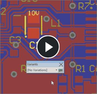
12 Design Variants, such as varied component parameters, will transfer to the PCB and be controlled by the Variant selector. Source URL:
Published on Online Documentation for Altium Products (
 Published on Online Documentation for Altium Products (https://www.altium.com/documentation) Home > Schematic Symbol Generation Tool Using Altium Documentation Modified by Jason Howie on Apr 11, 2017 Parent
Component Management in CircuitMaker
 Component Management in CircuitMaker Modified by Rob Evans on 14-Oct-2015 Related pages Driving a PCB Design through CircuitMaker Project Management Parent page: Exploring CircuitMaker A component is the
Class Structure in the PCB
 Class Structure in the PCB Old Content - visit altium.com/documentation Modified by on 13-Sep-2017 Related Videos Structured Classes in the PCB Editor Altium Designer already provided high-quality, robust
Libraries. Modified by Rob Evans on 15-Oct Related pages: Component Management in CircuitMaker
 Libraries Modified by Rob Evans on 15-Oct-2015 Related pages: Component Management in CircuitMaker From Idea to Manufacture - Driving a PCB Design through CircuitMaker Parent page: Panels Use the Libraries
Component Management in SOLIDWORKS PCB
 Component Management in SOLIDWORKS PCB Modified by Jason Howie on Oct 24, 2017 Parent page: Exploring SOLIDWORKS PCB A component is the general name given to a part that can be placed into an electronic
Published on Online Documentation for Altium Products (
 Published on Online Documentation for Altium Products (https://www.altium.com/documentation) Главная > Working with the Vaults Panel - Feature How-Tos Using Altium Documentation Modified by Jason Howie
Published on Online Documentation for Altium Products (
 Published on Online Documentation for Altium Products (https://www.altium.com/documentation) Главная > Working with the Explorer Panel - Feature How-Tos Using Altium Documentation Modified by Jason Howie
Fitted with modified component parameters, such as the component's value.
 Variants Modified by Susan Riege on Sep 4, 2018 Parent page: Exploring CircuitStudio The ability to create variations of the same base design is a real strength of CircuitStudio, and a tremendous productivity
Published on Online Documentation for Altium Products (
 Published on Online Documentation for Altium Products (https://www.altium.com/documentation) Home > Using Version Control Using Altium Documentation Modified by Rob Evans on Apr 11, 2017 RELATED INFORMATION
Altium Designer Viewer - Generating Output
 Altium Designer Viewer - Generating Output Old Content - visit altium.com/documentation Modified by on 6-Nov-2013 Altium Designer Viewer allows you to open, view, and generate output from, Output Job Configuration
Creating a Database Library from an Integrated Library
 Published on Online Documentation for Altium Products (https://www.altium.com/documentation) Home > Database Library Migration Tools Using Altium Documentation Modified by Jason Howie on Apr 11, 2017 Parent
Published on Online Documentation for Altium Products (
 Published on Online Documentation for Altium Products (https://www.altium.com/documentation) Home > Managed Schematic Symbols Using Altium Documentation Modified by Jason Howie on Jun 22, 2018 Parent page:
Published on Online Documentation for Altium Products (
 Published on Online Documentation for Altium Products (https://www.altium.com/documentation) Home > PCB - From-To Editor Using Altium Documentation Modified by Admin on Apr 11, 2017 Parent page: PCB Panels
Altium Designer Viewer - Viewing PCB Documents
 Altium Designer Viewer - Viewing PCB Documents Old Content - visit altium.com/documentation Modified by on 6-Nov-2013 In Altium Designer Viewer PCB documents are opened in the PCB Editor. The tools and
to be handled, tracked and verified, otherwise the components' designators and other design data can become out of sync.
 Understanding Design Annotation Old Content - visit altium.com/documentation Modified by Admin on Nov 6, 2013 This document explores the process of annotation in Altium Designer - from understanding Schematic,
Preparing the Board for Design Transfer. Creating and Modifying the Board Shape. Modified by Phil Loughhead on 15-Aug-2016
 Preparing the Board for Design Transfer Old Content - visit altium.com/documentation Modified by Phil Loughhead on 15-Aug-2016 This article describes how to prepare the new PCB file so that it is ready to
Defining Net Classes by Area on a Schematic. Creating a Net Class from a Blanket Directive. Modified by Admin on Sep 13, Blankets in Schematic
 Defining Net Classes by Area on a Schematic Old Content - visit altium.com/documentation Modified by Admin on Sep 13, 2017 Related Video Blankets in Schematic Altium Designer already allows you to create
Published on Online Documentation for Altium Products (
 Published on Online Documentation for Altium Products (https://www.altium.com/documentation) Home > PDN Analyzer Example Guide Using Altium Documentation Modified by Rob Evans on Dec 21, 2017 The PDN Analyzer
Releasing a Schematic Sheet to a Vault
 Releasing a Schematic Sheet to a Vault Old Content - see latest equivalent Modified by Jason Howie on 31-May-2017 Parent article: Design Content Management Being able to re-use design content is something
Published on Online Documentation for Altium Products (
 Published on Online Documentation for Altium Products (https://www.altium.com/documentation) Главная > Установка, лицензирование и управление системой Using Altium Documentation Modified by Jason Howie
Published on Online Documentation for Altium Products (
 Published on Online Documentation for Altium Products (https://www.altium.com/documentation) Home > Understanding Models, Components and Libraries Using Altium Documentation Modified by Phil Loughhead on
From Idea to Manufacture - Driving a PCB Design through SOLIDWORKS PCB
 From Idea to Manufacture - Driving a PCB Design through SOLIDWORKS PCB Modified by Jason Howie on 24-Oct-2017 Welcome to the world of electronic product development in Altium's world-class electronic design
Published on Online Documentation for Altium Products (
 Published on Online Documentation for Altium Products (https://www.altium.com/documentation) Home > Managed Simulation Models Using Altium Documentation Modified by Jason Howie on Jun 22, 2018 Parent page:
AltiumLive - Content Store
 AltiumLive - Content Store Frozen Content Modified by on 13-Sep-2017 Introducing the AltiumLive Content Store. The Content Store is an area in AltiumLive dedicated to content - content that is invaluable
Interactive 3D Measurement Tool
 Published on Online Documentation for Altium Products (https://www.altium.com/documentation) Home > 3D Measurements Using Altium Documentation Modified by Jason Howie on Apr 11, 2017 Interactive 3D Measurement
Schematic Libraries, Models and Integrated Libraries
 Published on Online Documentation for Altium Products (https://www.altium.com/documentation) Главная > A Look at Creating Library Components Using Altium Documentation Modified by Jason Howie on Apr 11,
PDN Analyzer Example Guide
 PDN Analyzer Example Guide Old Content - visit altium.com/documentation Modified by Admin on Nov 29, 2016 Related PDN Analyzer overview Overview video The PDN Analyzer application is relatively straightforward
PCB. Modified by Rob Evans on 28-May Parent page: PCB Panels
 PCB Modified by Rob Evans on 28-May-2015 Parent page: PCB Panels The PCB panel gives you full acces to board objects, items and classes via a filtered browser. Summary The PCB panel allows you to browse
From Idea to Manufacture - Driving a PCB Design through CircuitStudio
 From Idea to Manufacture - Driving a PCB Design through CircuitStudio Modified by Susan Riege on 13-Sep-2018 Welcome to the world of electronic product development in Altium's world-class electronic design
Tutorial - Getting Started with PCB Design
 Tutorial - Getting Started with PCB Design Old Content - visit altium.com/documentation Modified by Phil Loughhead on 3-Aug-2016 Welcome to the world of electronic product development environment in Altium
Attaching a Datasheet to a Component Item in the Vaults Panel
 Published on Online Documentation for Altium Products (https://www.altium.com/documentation) Home > Storing Component Datasheets in an Altium Vault Using Altium Documentation Modified by Jason Howie on
A Walk Through the Board Design Release Process
 A Walk Through the Board Design Release Process Frozen Content Modified by Jason Howie on 31-May-2017 Parent article: Board Design Release Altium's Design Data Management system includes a range of technologies
ActiveBOM - BOM Components
 ActiveBOM - BOM Components Old Content - visit altium.com/documentation Modified by on 13-Sep-2017 Parent article: ActiveBOM The BOM Components tab is a constituent part of the BOM document (*.BomDoc),
Releasing a Simulation Model to a Vault
 Releasing a Simulation Model to a Vault Old Content - see latest equivalent Modified by Jason Howie on May 31, 2017 Parent article: Vault-Based Domain Models From a designer's perspective, a vault-based
Editing Multiple Objects. Contents
 Editing Multiple Objects Contents Selecting Multiple Objects Inspecting the Objects Editing the Objects Editing Group Objects Step 1. Selecting the Capacitors Step 2. Changing the Comment String Step 3.
PCB. Summary. Modified by Rob Evans on 8-Oct Parent page: PCB Panels
 PCB Modified by Rob Evans on 8-Oct-2016 Parent page: PCB Panels The PCB panel gives you full access to board objects and items via a filtered browser. Summary The PCB panel allows you to browse the current
PCB Rules and Violations
 PCB Rules and Violations Old Content - visit altium.com/documentation Modified by on 6-Nov-2013 Parent page: Panels Browse, edit and interactively view design rules and their associated violations. Summary
magento_1:product-parts-finder
 magento_1:product-parts-finder https://amasty.com/docs/doku.php?id=magento_1:product-parts-finder For more details see the Product Parts Finder extension page. Product Parts Finder Setting up Finder step
Published on Online Documentation for Altium Products (http://www.altium.com/documentation)
") Published on Online Documentation for Altium Products (http://www.altium.com/documentation) Home > PCB Pad Via Templates A New Era for Documentation Modified on Apr 11, 2017 Parent page: PCB Panels The
Published on Online Documentation for Altium Products (http://www.altium.com/documentation) Home > PCB Pad Via Templates A New Era for Documentation Modified on Apr 11, 2017 Parent page: PCB Panels The
Generating Output for an Assembly Variant. Selecting the Variant. Modified by on 6-Nov-2013
 Generating Output for an Assembly Variant Old Content - visit altium.com/documentation Modified by on 6-Nov-2013 Assembly and/or report-based output for a variant is typically generated using an Output
Published on Online Documentation for Altium Products (
 Published on Online Documentation for Altium Products (https://www.altium.com/documentation) Home > Configuring PCB Printouts Using Altium Documentation Modified by Jason Howie on Apr 20, 2017 Print-based
Boot Camp-Special Ops Challenge Quiz
 1. What s the key difference between a panel and dialog window? a. There is none b. Panels must be closed in order to continue editing, whereas dialogs can be left open c. Dialogs must be closed in order
Published on Online Documentation for Altium Products (http://www.altium.com/documentation)
") Published on Online Documentation for Altium Products (http://www.altium.com/documentation) Home > Managed Projects Usability Improvements A New Era for Documentation Modified by Rob Evans on Apr 11, 2017
Published on Online Documentation for Altium Products (http://www.altium.com/documentation) Home > Managed Projects Usability Improvements A New Era for Documentation Modified by Rob Evans on Apr 11, 2017
Points Management. All user points in Locus Map are managed in Points manager. It can be accessed: from the main menu: from Functions panel:
 2018/11/17 11:22 1/30 All user points in Locus Map are managed in Points manager. It can be accessed: from the main menu: from Functions panel: Locus Map - knowledge base - http://docs.locusmap.eu/ Last
System Installation, Licensing & Management
 System Installation, Licensing & Management Old Content - visit altium.com/documentation Modified by on 13-Sep-2017 Installation of any software application should be straightforward, intuitive and, perhaps
Parameter. Parent page: Objects. Mod. ifi. Rob. Eva 25- Aug -20. Old Content - visit altium.com/documentation
 Parameter Old Content - visit altium.com/documentation Mod ifi ed by Rob Eva ns on 25- Aug -20 16 Parent page: Objects Parameters are used for components, documents and projects to add detail information
Generating Output for an Assembly Variant. Contents
 Generating Output for an Assembly Variant Contents Selecting the Variant Using an Output Job file Schematic prints Labeling the print with the variant name PCB assembly drawings Direct report generation
Installing SOLIDWORKS PCB
 Installing SOLIDWORKS PCB Modified by on 24-Oct-2017 Parent page: Installation Overview Installation of any software application should be straightforward, intuitive and, perhaps above all, fast. Furthermore,
PCB Layer Stack Management
 PCB Layer Stack Management Old Content - visit altium.com/documentation Modified by on 29-Nov-2016 Related Videos Define New Layer Stacks Layer Stack Regions A printed circuit board, or PCB, is used to mechanically
ActiveBOM - BOM Catalog
 ActiveBOM - BOM Catalog Old Content - visit altium.com/documentation Modified by Admin on Nov 29, 2016 Parent article: ActiveBOM The BOM Catalog tab is a constituent part of the BOM document (*.BomDoc),
Published on Online Documentation for Altium Products (https://www.altium.com/documentation)
") Published on Online Documentation for Altium Products (https://www.altium.com/documentation) Home > Defining the Layer Stack Using Altium Documentation Modified by Phil Loughhead on Apr 11, 2017 Related
Published on Online Documentation for Altium Products (https://www.altium.com/documentation) Home > Defining the Layer Stack Using Altium Documentation Modified by Phil Loughhead on Apr 11, 2017 Related
Using the PCB Component Wizard
 Published on Online Documentation for Altium Products (https://www.altium.com/documentation) Home > PCB Component Wizard Using Altium Documentation Modified by Phil Loughhead on Jun 19, 2017 The PCB Component
Building an Integrated Library
 Building an Integrated Library Old Content - visit altium.com/documentation Modified by on 6-Nov-2013 Integrated libraries combine schematic libraries with their related PCB footprints and/or SPICE and
Altium Designer Viewer. Contents
 Altium Designer Viewer Contents What You can do Key Features at-a-glance Supported Output Generation Viewer Environment Viewing Schematic Documents Viewing PCB Documents Searching Live Supplier Data Using
Working with the Board Insight System
 Working with the Board Insight System Old Content - visit altium.com/documentation Modified by on 29-Jul-2014 Board Insight is a configurable system of features that give you complete control over viewing
Published on Online Documentation for Altium Products (
 Published on Online Documentation for Altium Products (https://www.altium.com/documentation) Home > SnapSTEPModel Using Altium Documentation Modified by Jason Howie on Apr 11, 2017 Parent page: PCB Commands
Using Components Directly from Your Company Database
 Using Components Directly from Your Company Database Old Content - visit altium.com/documentation Modified by Phil Loughhead on 18-May-2016 This document provides detailed information on using components
Accessing the Interface
 Published on Online Documentation for Altium Products (https://www.altium.com/documentation) Главная > Browser-based Access & Management Using Altium Documentation Modified by Jason Howie on Jun 28, 2018
Libraries. Modified by Jason Howie on Oct 24, Parent page: IntegratedLibrary Panels
 Libraries Modified by Jason Howie on Oct 24, 2017 Parent page: IntegratedLibrary Panels Use the Libraries panel to access components in libraries currently available in SOLIDWORKS PCB. Summary The Libraries
Enhanced Polygon Editing and Management. Poured or Unpoured Polygons. Modified by Jason Howie on Nov 13, 2014
 Enhanced Polygon Editing and Management Old Content - visit altium.com/documentation Modified by Jason Howie on Nov 13, 2014 Most board designs today incorporate areas of copper, which are easily created
Accessing the Vault. Parent article: Altium Vault Technology. Mod. ifi. Adm. Sep 13,
 Frozen Content Mod ifi ed by Adm in on Sep 13, 201 7 Parent article: Altium Vault Technology This page contains information regarding browser-based access to the legacy Altium Vault Server. For browser-based
Specifying the PCB Design Rules and Resolving Violations
 Specifying the PCB Design Rules and Resolving Violations Summary This article introduces the PCB Design Rules System, in particular how rules are created and applied to objects in a design. It also describes
Figure 1. Output jobs are configured as an OutJob file, giving you full control over print-based output.
 PCB Printout Output Options Old Content - visit altium.com/documentation Modified by Admin on Sep 13, 2017 Print-based Output Print-based output for your PCB project in Altium Designer is available through
To learn more about a command, dialog, object or panel, press F1 when the cursor is over that item.
 Published on Online Documentation for Altium Products (https://www.altium.com/documentation) 主页 > 从理念到制造 通过Altium Designer推动PCB设计 Altium技术文档新纪元 Modified by Jun Chu on Apr 26, 2018 Welcome to the world
Published on Online Documentation for Altium Products (https://www.altium.com/documentation)
") Published on Online Documentation for Altium Products (https://www.altium.com/documentation) Главная > Local Version Control Service Using Altium Documentation Modified by Jason Howie on May 8, 2018 Parent
Published on Online Documentation for Altium Products (https://www.altium.com/documentation) Главная > Local Version Control Service Using Altium Documentation Modified by Jason Howie on May 8, 2018 Parent
A Suggested Methodology for Vault-Driven Electronics Design
 A Suggested Methodology for Vault-Driven Electronics Design Frozen Content Modified by Jason Howie on 31-May-2017 Additional Resources An Introduction to Vault-Driven Electronics Design Getting Started
For more detailed information on the differences between DelphiScript and Object Pascal, refer to the DelphiScript Reference document.
 Writing Scripts Old Content - visit altium.com/documentation Modified by on 13-Sep-2017 Related pages Script Editor Tools Scripting System Panels Parent page: Scripting Writing Scripts There a number of
IPC-7351B was released in 2010 and supersedes IPC-7351A (which was released in 2007).
.") IPC-7351B Compliance Old Content - visit altium.com/documentation Modified by Jason Howie on Nov 13, 2014 Altium Designer 14.3 incorporates a number of additions and enhancements to both the IPC Compliant
IPC-7351B Compliance Old Content - visit altium.com/documentation Modified by Jason Howie on Nov 13, 2014 Altium Designer 14.3 incorporates a number of additions and enhancements to both the IPC Compliant
Published on Online Documentation for Altium Products (
 Published on Online Documentation for Altium Products (https://www.altium.com/documentation) Home > Storage Manager Using Altium Documentation Modified by Jason Howie on Jun 16, 2017 Parent page: System
The following self-capacitance sensor types are available for use in your PCB designs:
 Support for Cypress Touch Controls Old Content - visit altium.com/documentation Modified by on 29-Nov-2016 Extending its support for the use of touch controls in designs, Altium Designer 15.1 provides
Moving to Altium Designer from Pads Logic and PADS Layout
 Moving to Altium Designer from Pads Logic and PADS Layout Old Content - visit altium.com/documentation Modified by on 13-Sep-2017 Translating complete PADS Logic and PADS Layout designs, including PCB,
Schematic Symbol Generation Tool
 Schematic Symbol Generation Tool Old Content - visit altium.com/documentation Modified by Rob Evans on May 4, 2015 The task of creating a component library symbol and its pin data has become an increasingly
Key Feature Summary: Altium Designer 14
 Altium Designer 14 Enhanced Layer Stack Manager The ability to define multiple, complex layer stacks in a single design. With different stack ups used in different regions of the PCB. With greater flexibility
An Insider's Guide to the Query Language
 An Insider's Guide to the Query Language Summary This article attempts to de-mystify what queries are, how and why they are used, and to provide insights into how these queries can be executed. An appendix
PCB. Parent page: Panels. Mod. ifi. 6Jan -20. Old Content - visit altium.com/documentation
 PCB Old Content - visit altium.com/documentation Mod ifi ed by on 6Jan -20 15 Parent page: Panels The PCB panel gives you full access to board objects, items and classes via a filtered browser. Summary
Flexslider v2.x Installation and User Manual
 2018/05/16 02:56 1/18 Latest version: 2.2.6 Compatibility: Magento 2.1.x, 2.2.x Disclaimer This is the installation and user manual for the Magento Flexslider v1.x extension created by Solide Webservices.
Summary. Parent Page: PCB Panels
 Published on Online Documentation for Altium Products (http://www.altium.com/documentation) 主页 > PCB - 3D Models Altium 技术文档新纪元 Modified by Annika Krilov on Apr 11, 2017 Parent Page: PCB Panels The 3D
Take Five and Update your Skills - Altium Designer Training Videos
 Whats New in Altium Designer 6.8 Frozen Content Modified by Admin on Sep 13, 2017 Summary {excerpt} Continuing to improve your productivity, Altium Designer 6.8 brings a new DxDesigner Importer as well
AltiumLive - Dashboard
 AltiumLive - Dashboard Frozen Content Modified by on 13-Sep-2017 Additional Resources FAQs Glossary When we purchase something, we like to (quite rightly) take ownership of, and control how, that something
PCB 3D Video. Making a PCB 3D Video. Modified by Admin on Sep 13, D PCB 'flyovers'
 PCB 3D Video Old Content - visit altium.com/documentation Modified by Admin on Sep 13, 2017 Related Videos 3D PCB 'flyovers' If a picture can 'tell a thousand words', it stands to reason that a series of
Published on Online Documentation for Altium Products (https://www.altium.com/documentation)
") Published on Online Documentation for Altium Products (https://www.altium.com/documentation) Главная > Офлайн-установка Altium Designer Using Altium Documentation Modified by Pavel Demidov on Apr 11, 2017
Published on Online Documentation for Altium Products (https://www.altium.com/documentation) Главная > Офлайн-установка Altium Designer Using Altium Documentation Modified by Pavel Demidov on Apr 11, 2017
Baseline dimension objects are available for placement in the PCB Editor only, by clicking Home
 Baseline Dimension Modified by Jason Howie on 24-Oct-2014 Parent page: Dimension A placed Baseline Dimension. Summary A baseline dimension is a group design object. It allows for the dimensioning of a
Moving to Altium Designer from Protel 99 SE
 Moving to Altium Designer from Protel 99 SE Summary This article outlines the process you go through to transfer a Protel 99 SE design into the Altium Designer environment. Protel 99 SE uses the design
How to Simplify PCB Design
 How to Simplify PCB Design 1. 2. 3. 4. HOW TO SIMPLIFY AND AUTOMATE YOUR PCB ECO WORKFLOW HOW TO SIMPLIFY ROUTING WITH PIN SWAPPING HOW TO SIMPLIFY OUTPUT GENERATION WORKFLOW HOW TO SIMPLIFY CIRCUIT REPLICATION
Creating a Multi-channel Design
 Creating a Multi-channel Design Summary This tutorial shows how to create a multichannel design in the Schematic Editor, including the use of subsheets, sheet symbols and the Repeat keyword. Setting room
An Insiders Guide to the Query Language. Understanding Queries. Data Filtering - facilitating editing tasks. Modified by on 6-Nov-2013
 An Insiders Guide to the Query Language Old Content - visit altium.com/documentation Modified by on 6-Nov-2013 This document attempts to de-mystify what queries are, how and why they are used, and to provide
1, 2, 4 and 8-Channel Very Low Capacitance ESD Protectors
 1, 2, 4 and 8-Channel Very Low Capacitance ESD Protectors CM1210 Features 1,2,4 and 8 channels of ESD protection Very low loading capacitance (1.0pF typical) ±6 kv ESD protection per channel (IEC 61000-4-2
Comments. Summary. Modified by Rob Evans on Jun 10, Parent page: Workspace Manager Panels
 Comments Modified by Rob Evans on Jun 10, 2015 Parent page: Workspace Manager Panels The Comments panel showing a collection of user comments for the currently active project. Summary The Comments panel
Information for IT Departments
 Information for IT Departments Frozen Content Modified by Admin on Sep 13, 2017 This page contains information regarding legacy Altium Vault Technologies - namely the Altium Vault Server and Altium Personal
Moving to Altium Designer from Protel 99 SE. Contents
 Moving to Altium Designer from Protel 99 SE Contents Design Database Become a Design Workspace & Projects Importing a 99 SE Design Database Creating the Altium Designer Project(s) Manually Adding and Removing
Published on Online Documentation for Altium Products (
 Published on Online Documentation for Altium Products (https://www.altium.com/documentation) Home > Simulation Profiles Using Altium Documentation Modified by Jason Howie on Dec 14, 2017 Along with other
Parent page: PCB Panel
 Published on Online Documentation for Altium Products (https://www.altium.com/documentation) 主页 > PCB Library Using Altium Documentation Modified by Annika Krilov on Apr 11, 2017 Parent page: PCB Panel
SEO Toolkit for Magento 2
 Last update: 2017/09/04 20:04 magento_2:seo_toolkit https://amasty.com/docs/doku.php?id=magento_2:seo_toolkit For more details see the SEO Toolkit for Magento 2 extension page. SEO Toolkit for Magento
Text strings are available for placement in both Schematic and Schematic Library Editors by:
 Text String Old Content - visit altium.com/documentation Modified by on 20-Nov-2013 Parent page: Objects A placed Text String. Summary A text string (also referred to as an annotation) is a non-electrical
This document provides detailed information on placing components from a database using Altium Designer's SVN Database Library feature.
 Old Content - visit altium.com/documentation Mod ifi ed by on 13- Sep -20 17 This document provides detailed information on placing components from a database using Altium Designer's SVN Database Library
Part. Summary. Modified by Susan Riege on Aug 5, Parent page: Objects
 Part Old Content - visit altium.com/documentation Modified by Susan Riege on Aug 5, 2016 Parent page: Objects Related Resources Net Ties and How to Use Them (PDF) The Part represents the actual physical
PCB Filter. Summary. Panel Access. Modified by Admin on Dec 12, PCB Inspector. Parent page: Panels
 PCB Filter Old Content - visit altium.com/documentation Modified by Admin on Dec 12, 2013 Related panels PCB Inspector Parent page: Panels Quickly locate and highlight objects using logical queries in
Configuration Starting the CoDaBix Compact Application General... 2 (1) CoDaBix CompactToolbar... 2 Licence Dialog... 3
 CoDaBix CompactToolbar... 2 Licence Dialog... 3") 1/2 Table of Contents... 1 Starting the CoDaBix Compact Application... 1 Configuration... 1 General... 2 (1) CoDaBix CompactToolbar... 2 Licence Dialog... 3 About... 3 (2) Working Area... 4 (3) Title Bar...
1/2 Table of Contents... 1 Starting the CoDaBix Compact Application... 1 Configuration... 1 General... 2 (1) CoDaBix CompactToolbar... 2 Licence Dialog... 3 About... 3 (2) Working Area... 4 (3) Title Bar...
Creating a Multi-board Assembly
 Published on Online Documentation for Altium Products (https://www.altium.com/documentation) 主页 > Creating the Physical Multi-board Assembly Using Altium Documentation Modified by Susan Riege on Mar 23,
250 Mbps Transceiver in LC FB2M5LVR
 250 Mbps Transceiver in LC FB2M5LVR DATA SHEET 650 nm 250 Mbps Fiber Optic Transceiver with LC Termination LVDS I/O IEC 61754-20 Compliant FEATURES LC click lock mechanism for confident connections Compatible