A Brief History of Atom Probe
|
|
|
- Mary Perry
- 5 years ago
- Views:
Transcription


1 A Brief History of Atom Probe Thomas F. Kelly and John A. Panitz Pre-meeting Congress, M&M 2016
2 Ancestry of the Modern Atom Probe 2

: Father")
3 Erwin Wilhelm Müller Photograph of Professor Erwin W. Müller ( ): Father of High Field Nanoscience 3

4 1935 Field Electron Emission Microscopy - electron E + Fluorescent Screen E. W. Müller, Z. Phys. 120 (1943) 270 4
5 Field Electron Emission Microscopy Field electron emission microscopy (FEEM) was developed as a point projection microscope FEEM patterns showed clear crystallographic information Ba atoms and phthalocyanine molecules were observed on W needles with FEEM Image resolution improved through the late 1940 s Müller sought to resolve atoms with FEEM Eventually it was concluded that FEEM would resolve no better than ~2 nm Field desorption (and evaporation?) was shown in
 had higher")
6 FEEM tips were routinely cleaned by reversing the bias Practitioners of FEEM noticed: Field ions were emitted during reverse bias Müller sought, and found, a way to increase the signal of field ions: H, He gas Intensity of field ion signal varied with gas pressure In early 1950s, this was pursued for imaging the tip surface Atoms at ledges were seen Early field ion images (FIM) had higher resolution than FEEM Field Ion Microscopy Erwin Müller at Penn State 6


7 1951 Field Ion Microscopy Gas supply + ion Fluorescent Screen + E First images ever of atoms (on ledges of tip surface): Summer 1951, Müller First atomically resolved lattice on surface: October 11, 1955, Bahadur and Müller 7

8 Surface atoms and defects are visible in FIM E.g. Self-interstitial atoms produce large image in FIM Imaging Crystal Defects in FIM 8

9 Vacancies imaged in FIM! Vacancies observed Knock-on damage cascades were mapped by cinematography of FIM 9


10 1960s FIM 10

11 40 K Tungsten Needle Helium Gas Phosphor Screen FIM & Field Evaporation Movie Best Imaging Voltage Slight Laser Heating Field Evaporation Adsorbed gas atoms field ion image Specimen atoms atom probe Movie Courtesy Baptiste Gault

12 3D FIM Comes to Life! 100% of atoms positioned High precision on atom locations Crystal structure and defects readily visible 12
, the bright dots are individual boron atoms that have segregated to a grain boundary (arrowed).")
13 Compositional Contrast in FIM In this field ion micrograph of boron-doped nickel aluminide (Ni 3 Al), the bright dots are individual boron atoms that have segregated to a grain boundary (arrowed). 13


14 Müller sought a way to identify atoms in the specimen Barofsky was asked to built a magnetic sector mass spectrometer He later suggested that they should try ToF Panitz was assigned the job How to detect single atoms? Never been done The Atom Probe John A. Panitz Mueller, Panitz, McLane, Rev. Sci. Instrum. (1968) vol. 39, p

15 Much of the following from Panitz th International Field Emission Symposium Atom Probe Tomography and Microscopy Stuttgart, Germany

16 The Müller Group ~ 1968 Names in bold are part of the atom probe effort 16

17 1967 Original Atom-Probe Field Ion Microscope 17

18 Single Atom Detection Was Invented Photograph of oscilloscope screen 18

19 Data File: Oscilloscope Trace Polaroid picture of oscilloscope screen Atom Hit 19

20 First Publication on Atom Probe 20

21 The Second Atom Probe

22 Muller and Panitz 22

23 Imaging Atom Probe: the Progenitor of Atom Probe Tomography MRP of 14 was achieved! Tip tilting not needed Flight distance cm to center Observe field ion image or field desorption image Mass analyze all atoms within a field of view 23

24 Imaging Atom Probe 2.0: Curved MCPs Tip at center of MCP curvature All parts of detector have same flight length High mass resolution over entire field of view Tomographic imaging possible Detector technology for recording each ion impact position was not yet invented 24


25 Field Desorption Images of Single Specie Time gate on MCPs 25

26 Pulsed Laser Atom Probe A laser was adapted to the Imaging atom probe at Sandia Laboratories First time non-metals were atom probed Laser pulsing has become the dominant pulsing mode in APT 26
27 PLAP data - Molybdenum Flight path was not optimized No correction for flight distance across detector Demonstrated laser pulsing for metals, insulators Correct isotopic abundances 27


28 New Groups Develop University of Oxford Professor George Smith Congratulations to George MSA Distinguished Scientist Award First atom probe expert Early atom probe at Oxford 28

29 1975 The Vacuum Generators APFIM 100 Developed in conjunction with Smith et al. at Oxford First commercial atom probe 29


30 1988 The Position-Sensitive Atom Probe Adapted a Wedge-and-Strip detector from astronomy to a VG APFIM Fall MRS presented by George Smith First operational 3DAP 30


31 The Position-Sensitive Atom Probe (PoSAP) 31
32 The Commercial PoSAP Manufactured by Kindbrisk (Oxford NanoScience) 32


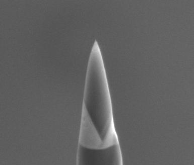
33 Tomographic Atom Probe D. Blavette, A. Bostel, J. M. Sarrau, B. Deconihout, and A. Menand: An atom-probe for three dimensional tomography. Nature 363: (1993). 33


34 TAP Detector 34
35 Electron-Beam-Pulsed Atom Probe Thermal pulsing can be route to high repetition rates Need to heat very small volumes for rapid cooling Needed for high mass resolving power Electron beams can be focused to very small diameter ~100 nm heated volume Specimen in atom probe is positive electrode Thermal pulsing with electron beam 35
36 Atom Probe and (S)TEM Electron beam pulsing and atom probe naturally suggest imaging during analysis There are many advantages of having a TEM image of the specimen Kelly, 1990 IFES meeting, Albuquerque 36
37 Electron-Beam-Pulsed Atom Probe Larson, Camus and Kelly, Applied Surface Science 67 (1993)

38 The Atom Probe Microscope 38


39 There were Challenges to overcome Vibration-free cooling Field emission from electrode With Cryopump on 39
40 Scanning Atom Probe Nishikawa, O., Kimoto, M., Applied Surface Science (1994) vol. 76, pp
41 Basic conundrum: Origins of Local Electrode Atom Probe 3DAP is superlative analytical tool but 3DAP of 1990 is too slow to be practical (1 atom/s) The field of view was limited to about 20 nm Scanning Atom Probe used an aperture electrode close to specimen Field emitter arrays had demonstrated field enhancement factors of 10 relative to remote electrode Lower voltage pulsers can achieve much higher repetition rates Two key results: Use local electrode to obtain high data rates Relative reduction in energy spread can be compensated by post A Brief History of Atom Probe acceleration => high mass resolution over full field of view July 24,

42 Local Electrode Specimen Local Electrode Enables: Analysis of microtips and needles High data collection rates Large field of view 42


43 Microtips in the LEAP 1 mm Local Electrode Microtip Array Sharp Flat Top 43

44 Solid Model of Alpha Prototype Cryopump Specimen and local electrode Detector 44

45 Alpha Prototype to LEAP 3000 Circa

46 The LEAP 4000 X
47 Near Full page on gradient background The LEAP
48 There Are Many LEAP Models Anticipated Quantum LEAP LEAP Frog LEAP of Faith Lambeau LEAP 48


49 EIKOS IS Atom Probe Tomography July 24, 2016


 1 a)")
 c) d )")
 David")


50 Focused Ion Beam: General Liftout Method a) b) 1 a) b) 3 2 c) d) c) d ) e) f) e) f) David Larson led the way on FIB preparation of specimens All scale bars are 5 μm All scale bars are 1 μm (except f which is 200nm) 50


 179.")
51 STEM+LEAP The ATOM Project Build objective lens assembly with atom probe inside Position Sensitive Detector O. Krivanek et al., Ultramicros. 108 (2008) 179. Side-entry liquid He sample stage 51


52 TEM+LEAP Project Tomo Build objective lens assembly with atom probe inside 52

53 Specimen Holder for Project TOMO Electron Beam Evaporated Ions 53


54 AST EELS Atomic Structure Electronic Structure Electronic Structure Atom Probe Diffraction ASAT STEM Computed Image Properties Structure-Properties Microscopy
55 In the History of Microscopy, We are at an Inflection Point Log (Length Scale of Knowledge) Mega Macro Micro Prehistory Human eye Telescopes Microscopes 1600 Today Time Inflection point 55
56 The History of Microscopy The history of microscopy is the pursuit of learning more and more about less and less We have reached the atomic scale This marks an inflection point The future of microscopy will be the pursuit of learning more and more about more and more 56

57 Ancestry of the Modern Atom Probe 57


58 We ve made progress: From Müller FEM FIM APFIM 58
59 To Commercial Atom Probes 1975 VG APFIM PoSAP 2016 LEAP 5000, EIKOS 59
60 D Atomic-Scale Tomography, an Achievable Vision January 26,
Delayline Detectors. Imaging Detection of Electrons, Ions & Photons with Picosecond Time Resolution. e - I +
 Delayline Detectors Imaging Detection of Electrons, Ions & Photons with Picosecond Time Resolution e - I + Delayline Readout of MCPs - The Technical Approach - Microchannel-Plate (MCP) detectors provide
Advanced materials research using the Real-Time 3D Analytical FIB-SEM 'NX9000'
 SCIENTIFIC INSTRUMENT NEWS 2017 Vol. 9 SEPTEMBER Technical magazine of Electron Microscope and Analytical Instruments. Technical Explanation Advanced materials research using the Real-Time 3D Analytical
Spherical Crystal X-ray Imaging for MTW, OMEGA, and OMEGA EP
 Spherical Crystal X-ray Imaging for MTW, OMEGA, and OMEGA EP C.STOECKL, G. FISKEL, R. K. JUNGQUIST, P. M. NILSON, AND W. THEOBALD University of Rochester, Laboratory for Laser Energetics Spherical Crystal
MATERIALS CHARACTERIZATION FACILITY
 MATERIALS CHARACTERIZATION FACILITY LOOK DEEPER AT THE GEORGIA TECH MATERIALS CHARACTERIZATION FACILITY Shared Imaging Facilities & Analytical Services Available to academic, industry, and government users,
Exam Microscopic Measurement Techniques 4T th of April, 2008
 Exam Microscopic Measurement Techniques 4T300 29 th of April, 2008 Name / Initials: Ident. #: Education: This exam consists of 5 questions. Questions and sub questions will be rewarded with the amount
Microscopy. Marc McGuigan North Quincy High School Thursday, May 11, 2006
 Microscopy Marc McGuigan North Quincy High School Thursday, May 11, 006 Outline Activity Introduction Electromagnetic Spectrum Visible Light Light Microscope AFM Scanning Electron Microscopy Near-Field
Field Evaporation Simulation of a Cross Section ABA Structure
 Field Evaporation Simulation of a Cross Section ABA Structure David J. Larson & Brian P. Geiser www.cameca.com Acknowledgements T. Kelly, T. Prosa, D. Reinhard, R. Ulfig, P. Clifton, E. Oltman etc. (Cameca)
TIME OF FLIGHT Components from:
 TIME OF FLIGHT Components from: JORDAN TOF PRODUCTS, INC. 990 Golden Gate Terrace Grass Valley, CA 95945 Phone: (530) 272-4580 Fax: (530) 272-2955 Web: www.rmjordan.com Email: info@rmjordan.com INSTRUCTION
CHEM-E5225 :Electron Microscopy Imaging I
 CHEM-E5225 :Electron Microscopy Imaging I 2018.11 Yanling Ge Outline Amplitude Contrast Phase Contrast Images Thickness and Bending Effects Amplitude Contrast Amplitude phase TEM STEM Incoherent elastic
diffraction patterns obtained with convergent electron beams yield more information than patterns obtained with parallel electron beams:
 CBED-Patterns Principle of CBED diffraction patterns obtained with convergent electron beams yield more information than patterns obtained with parallel electron beams: specimen thickness more precise
Confocal Microscopy Imaging of Single Emitter Fluorescence and Hanbury Brown, and Twiss Setup for Photon Antibunching. Abstract
 James Maslek 10/26/12 Confocal Microscopy Imaging of Single Emitter Fluorescence and Hanbury Brown, and Twiss Setup for Photon Antibunching Abstract The purpose of this experiment was to observe fluorescence
JSM-7900F. Scientific / Metrology Instruments. Schottky Field Emission Scanning Electron Microscope. Ultimate Analytical tool
 Scientific / Metrology Instruments Schottky Field Emission Scanning Electron Microscope Ultimate Analytical tool JSM-7900F High-Performance FE-SEM successfully combining ultrahigh resolution and unprecedented
The NEWSLETTER Autumn 2014
 Advanced Thermal Measurements and Modelling to Improve Polymer Process Simulations By J.Sweeney,M.Babenko, G.Gonzalez, H.Ugail and B.R.Whiteside, S.Bigot, F.Lacan, H.Hirshy, P.V.Petkov, Polymer IRC, School
CSCI 4974 / 6974 Hardware Reverse Engineering. Lecture 14: Invasive attacks
 CSCI 4974 / 6974 Hardware Reverse Engineering Lecture 14: Invasive attacks Attack types Semi-invasive Device is depackaged, but die isn't damaged Invasive Any attack involving physical damage to die Semi-invasive
Introduction of Hitachi SU1510
 Introduction of Hitachi SU1510 1 1. Main Features of the SU1510 SU1510 Same high-performance optics as S-3400N Variable Pressure mode as standard Large samples up to 153mm in diameter (observation range
Confocal Microscope Imaging of Single-Emitter Fluorescence and Hanbury Brown & Twiss Setup for Photon Antibunching. Edward Pei
 Confocal Microscope Imaging of Single-Emitter Fluorescence and Hanbury Brown & Twiss Setup for Photon Antibunching Edward Pei Abstract The purpose of these labs was to study single photon sources and measure
STEM electron tomography in the Scanning Electron Microscope
 Journal of Physics: Conference Series PAPER OPEN ACCESS STEM electron tomography in the Scanning Electron Microscope To cite this article: M Ferroni et al 2015 J. Phys.: Conf. Ser. 644 012012 Recent citations
Lecture 02 Microscopy, Staining, Classification (Ch3)
") Lecture 02 Microscopy, Staining, Classification (Ch3) Topics Methods of Culturing Microorganisms Microscope (History, Types, Definitions) Staining (Gram s) Dichotomous keys Micro for Health Sciences 1
Lecture 02 Microscopy, Staining, Classification (Ch3) Topics Methods of Culturing Microorganisms Microscope (History, Types, Definitions) Staining (Gram s) Dichotomous keys Micro for Health Sciences 1
specular diffuse reflection.
 Lesson 8 Light and Optics The Nature of Light Properties of Light: Reflection Refraction Interference Diffraction Polarization Dispersion and Prisms Total Internal Reflection Huygens s Principle The Nature
Two slit interference - Prelab questions
 Two slit interference - Prelab questions 1. Show that the intensity distribution given in equation 3 leads to bright and dark fringes at y = mλd/a and y = (m + 1/2) λd/a respectively, where m is an integer.
CHAPTER 2 MEDICAL IMAGING WITH NON-IONIZING RADIATION
 CHAPTER 2 MEDICAL IMAGING WITH NON-IONIZING RADIATION 1 Ultrasound Imaging 1.1 Ultrasound Production and Detection Ultrasound is frequency vibration. To produce and detect ultrasound, we use crystals which
Xuechang Ren a *, Canhui Wang, Yanshuang Li, Shaoxin Shen, Shou Liu
 Available online at www.sciencedirect.com Physics Procedia 22 (2011) 493 497 2011 International Conference on Physics Science and Technology (ICPST 2011) Optical Tweezers Array System Based on 2D Photonic
High-Accuracy LIBS with Nanosecond and Picosecond Time Resolution Enabled by Ultrasensitive emiccd Technology
 2015 Princeton Instruments, Inc. All rights reserved. High-Accuracy LIBS with Nanosecond and Picosecond Time Resolution Enabled by Ultrasensitive emiccd Technology The PI-MAX4:1024EMB emiccd camera seamlessly
3D Energy Dispersive Spectroscopy Elemental Tomography in the Scanning Transmission Electron Microscope
 3D Energy Dispersive Spectroscopy Elemental Tomography in the Scanning Transmission Electron Microscope Brian Van Devener Topics 1.Introduction to EDS in the STEM 2.Extending EDS into three dimensions
Chapter 24. Wave Optics
 Chapter 24 Wave Optics Wave Optics The wave nature of light is needed to explain various phenomena Interference Diffraction Polarization The particle nature of light was the basis for ray (geometric) optics
A SUPER-RESOLUTION MICROSCOPY WITH STANDING EVANESCENT LIGHT AND IMAGE RECONSTRUCTION METHOD
 A SUPER-RESOLUTION MICROSCOPY WITH STANDING EVANESCENT LIGHT AND IMAGE RECONSTRUCTION METHOD Hiroaki Nishioka, Satoru Takahashi Kiyoshi Takamasu Department of Precision Engineering, The University of Tokyo,
HKL Flamenco EBSD Data Acquisition Flow
 HKL Flamenco EBSD Data Acquisition Flow Basic steps for automatic data acquisition (e.g. orientation mapping) This is basic routine for the new operator. Feel free to experiment with different settings
Vision Based Metal Spectral Analysis using
 1/27 Vision Based Metal Spectral Analysis using Eranga Ukwatta Department of Electrical and Computer Engineering The University of Western Ontario May 25, 2009 2/27 Outline 1 Overview of Element Spectroscopy
Durham Magneto Optics Ltd. NanoMOKE3
 Durham Magneto Optics Ltd NanoMOKE3 Specifications Marketed by Quantum Design 1 1. Introduction NanoMOKE3 is a new generation of ultra-high sensitivity magnetooptical magnetometer and Kerr microscope.
2D-CMOS Detector ELECTRON DETECTOR WITH HIGH SPEED CMOS. Key Features
 ELECTRON DETECTOR WITH HIGH SPEED CMOS CAMERA AND Graphics PROCESSING UNIT Key Features MCP Chevron assembly with fast phosphorous screen High speed CMOS camera Parallel true pulse counting by Graphics
Scanned by CamScanner
 Scanned by CamScanner Scanned by CamScanner Annexure I Name of the equipment: Field Emission Scanning Electron Microscope (FE-SEM) along with Energy Dispersive Spectroscope (EDS) and accessories. Technical
Intermediate Physics PHYS102
 Intermediate Physics PHYS102 Dr Richard H. Cyburt Assistant Professor of Physics My office: 402c in the Science Building My phone: (304) 384-6006 My email: rcyburt@concord.edu My webpage: www.concord.edu/rcyburt
12/7/2012. Biomolecular structure. Diffraction, X-ray crystallography, light- and electron microscopy. CD spectroscopy, mass spectrometry
 phase difference at a given distance constructive/destructive interference Biomolecular structure. Diffraction, X-ray crystallography, light- and electron microscopy. CD spectroscopy, mass spectrometry
ENVISION A NEW WAY OF COMBINED COMPETENCIES
 Carl Zeiss SMT Nano Technology Systems Division ENVISION A NEW WAY OF COMBINED COMPETENCIES ZEISS NVision 40 The new 3D CrossBeam Workstation that combines FIB and GEMINI SEM columns to a unique system
Single-particle electron microscopy (cryo-electron microscopy) CS/CME/BioE/Biophys/BMI 279 Nov. 16 and 28, 2017 Ron Dror
 CS/CME/BioE/Biophys/BMI 279 Nov. 16 and 28, 2017 Ron Dror") Single-particle electron microscopy (cryo-electron microscopy) CS/CME/BioE/Biophys/BMI 279 Nov. 16 and 28, 2017 Ron Dror 1 Last month s Nobel Prize in Chemistry Awarded to Jacques Dubochet, Joachim Frank
Single-particle electron microscopy (cryo-electron microscopy) CS/CME/BioE/Biophys/BMI 279 Nov. 16 and 28, 2017 Ron Dror 1 Last month s Nobel Prize in Chemistry Awarded to Jacques Dubochet, Joachim Frank
Lecture: P1_Wk3_L5 Contact Mode Scans. Ron Reifenberger Birck Nanotechnology Center Purdue University 2012
 Lecture: Contact Mode Scans Ron Reifenberger Birck Nanotechnology Center Purdue University 2012 1 The Purpose of a Microscope is to Obtain an Image Reflected laser spot Laser Diode Four-Quadrant Photodetector
Reflections from a thin film
 Reflections from a thin film l Part of the wave reflects from the top surface and part from the bottom surface l The part that reflects from the top surface has a 180 o phase change while the part that
f. (5.3.1) So, the higher frequency means the lower wavelength. Visible part of light spectrum covers the range of wavelengths from
 So, the higher frequency means the lower wavelength. Visible part of light spectrum covers the range of wavelengths from") Lecture 5-3 Interference and Diffraction of EM Waves During our previous lectures we have been talking about electromagnetic (EM) waves. As we know, harmonic waves of any type represent periodic process
Lecture 5-3 Interference and Diffraction of EM Waves During our previous lectures we have been talking about electromagnetic (EM) waves. As we know, harmonic waves of any type represent periodic process
NDD FLIM Systems for Leica SP2 MP and SP5 MP Multiphoton Microscopes
 NDD FLIM Systems for Leica SP2 MP and SP5 MP Multiphoton Microscopes bh FLIM systems for the confocal and the multiphoton versions of the Leica SP2 and SP5 microscopes are available since 2002 [4]. These
Topic 02 Microscopy, Staining, Classification (Ch3)
") Topic 02 Microscopy, Staining, Classification (Ch3) Topics Dichotomous keys Methods of Culturing Microorganisms (9.6) Microscope (History, Types, Definitions) Staining (Gram s) (2.4) Micro for Health Sciences
Topic 02 Microscopy, Staining, Classification (Ch3) Topics Dichotomous keys Methods of Culturing Microorganisms (9.6) Microscope (History, Types, Definitions) Staining (Gram s) (2.4) Micro for Health Sciences
A CAMERA SHUTTER USED IN HIGH RESOLUTION BUBBLE CHAMBER PHOTOGRAPHY* J. D. Ferrie, R. C. Field and D. A. Talaska
 SLAC-PUB-2905 April 1982 (El A CAMERA SHUTTER USED IN HIGH RESOLUTION BUBBLE CHAMBER PHOTOGRAPHY* J. D. Ferrie, R. C. Field and D. A. Talaska Stanford Linear Accelerator Center Stanford University, Stanford,
Thread Mountable Cameo Laser Diode Module
 Thread Mountable Cameo Laser Diode Module Thread Mountable Cameo The Cameo is a unique, versatile, high quality industrial laser diode module widely used in alignment applications. Available in two models,
Modeling ion extraction from a free-plasma surface with a flexible conformal mesh
 Modeling ion extraction from a free-plasma surface with a flexible conformal mesh STANLEY HUMPHRIES JR. Field Precision, PO Box 13595, Albuquerque, New Mexico 87192 Abstract This paper describes a new
A Global Laser Brand. Versatile Module
 A Global Laser Brand Versatile Module The Versatile Module The VM (Versatile Module) from Imatronic provides a high quality and cost effect OEM solution to a wide range of applications including Machine
Scanning Capacitance Microscopy Investigations of Focused Ion Beam Damage in Silicon
 Scanning Capacitance Microscopy Investigations of Focused Ion Beam Damage in Silicon W. Brezna, H. Wanzenböck, A. Lugstein, E. Bertagnolli, E. Gornik, J. Smoliner Institute for Solid State Electronics,
Physics 625 Femtosecond laser Project
 Physics 625 Femtosecond laser Project The purpose of this project is for each person to gain experience in designing part of a femtosecond laser system for pump-probe experiments. The system diagram is
Cover Page. The handle holds various files of this Leiden University dissertation
 Cover Page The handle http://hdl.handle.net/1887/48877 holds various files of this Leiden University dissertation Author: Li, Y. Title: A new method to reconstruct the structure from crystal images Issue
A Global Laser Brand. Gated Cameo
 A Global Laser Brand The is a miniature laser diode module that has a threaded barrel for easy bulkhead mounting which ensures good thermal contact between module and heat sink. This new concept in laser
Hardware Update. John Jayne 5 th AMS User s Meeting 10/11/04
 Hardware Update John Jayne 5 th AMS User s Meeting 10/11/04 Hardware TOF AMS Light Scattering module Short chamber Beam Width Probe High pressure lens for larger size particles Rigid critical aperture
12 Feb 19. Images and text courtesy of John Bean, University of Virginia
 Here we take the covers off the atomic force microscope. Inside, there is a circuit board that controls and monitors the probe s movement. The probe, itself, is under the cover at the right. 1 2 The probe
Sample Introduction Systems SOLID LASER ABLATION
 Sample Introduction Systems SOLID LASER ABLATION Laser ablation Benefits: spatial resolution of < 10 um little to no sample preparation required Drawbacks: transient signal reduced precision/accuracy relative
Chapter 38. Diffraction Patterns and Polarization
 Chapter 38 Diffraction Patterns and Polarization Diffraction Light of wavelength comparable to or larger than the width of a slit spreads out in all forward directions upon passing through the slit This
Sonicator -Standard Operating Procedure [Updated September 10, 2014] Location of Machine: Composites Lab - Nanoparticle Containment Room, RFM 1218
![Sonicator -Standard Operating Procedure [Updated September 10, 2014] Location of Machine: Composites Lab - Nanoparticle Containment Room, RFM 1218](/thumbs/96/126856320.jpg "Sonicator -Standard Operating Procedure [Updated September 10, 2014] Location of Machine: Composites Lab - Nanoparticle Containment Room, RFM 1218") Sonicator Vibra-Cell Autotune Series 750 Watt Model Location of Machine: Composites Lab - Nanoparticle Containment Room, RFM 1218 Location of SOP and Machine Operating & Safety Manual: Composites Lab website
Sonicator Vibra-Cell Autotune Series 750 Watt Model Location of Machine: Composites Lab - Nanoparticle Containment Room, RFM 1218 Location of SOP and Machine Operating & Safety Manual: Composites Lab website
Condenser Optics for Dark Field X-Ray Microscopy
 Condenser Optics for Dark Field X-Ray Microscopy S. J. Pfauntsch, A. G. Michette, C. J. Buckley Centre for X-Ray Science, Department of Physics, King s College London, Strand, London WC2R 2LS, UK Abstract.
HIGH RESOLUTION COMPUTED TOMOGRAPHY FOR METROLOGY
 HIGH RESOLUTION COMPUTED TOMOGRAPHY FOR METROLOGY David K. Lehmann 1, Kathleen Brockdorf 1 and Dirk Neuber 2 1 phoenix x-ray Systems + Services Inc. St. Petersburg, FL, USA 2 phoenix x-ray Systems + Services
General Physics Experiment 11
 Physics Labs General Physics Experiment 11 Interference and Diffraction of Light Objectives: To measure the wavelength of light emitted by a Helium-Neon laser. To observe the character of single slit diffraction.
NanoScale Storage Systems Inc.
 NanoScale Storage Systems Inc. NanoTechnology for Hard Disk Drives Joe Straub 7100 Nanjemoy CT Falls Church VA 22046-3851 Phone: +1-703-241-0882 FAX: +1-703-241-0735 E-mail: joseph.straub@verizon.net Presented
Programming Characteristics on Three-Dimensional NAND Flash Structure Using Edge Fringing Field Effect
 JOURNAL OF SEMICONDUCTOR TECHNOLOGY AND SCIENCE, VOL.14, NO.5, OCTOBER, 2014 http://dx.doi.org/10.5573/jsts.2014.14.5.537 Programming Characteristics on Three-Dimensional NAND Flash Structure Using Edge
Diffraction and Interference
 Experiment #32 Diffraction and Interference Goals: Perform a quantitative investigation of two-slit interference Explore use of a photodiode to measure light intensity References 1. I. G. Main, Vibrations
Detector systems for light microscopy
 Detector systems for light microscopy The human eye the perfect detector? Resolution: 0.1-0.3mm @25cm object distance Spectral sensitivity ~400-700nm Has a dynamic range of 10 decades Two detectors: rods
Precise Eye High Mag Fixed Lenses
 Precise Eye High Mag Fixed Lenses High resolution, diffraction-limited f/4.5 optical quality for high precision measurement and inspection. Long working distance makes illumination and handling easier.
The diffraction pattern from a hexagonally-shaped hole. Note the six-fold symmetry of the pattern. Observation of such complex patterns can reveal
 The diffraction pattern from a hexagonally-shaped hole. Note the six-fold symmetry of the pattern. Observation of such complex patterns can reveal the underlying symmetry structure of the object that diffracts
Introduction of the Industry's Broadest Tunable Quantum Cascade Lasers. February Block Engineering 1
 Introduction of the Industry's Broadest Tunable Quantum Cascade Lasers February 2014 2014 Block Engineering 1 Widely-Tunable QCL Products LaserTune Mini-QCL Smallest widely-tunable QCL source Embedded
Polarization of Light
 From http://micro.magnet.fsu.edu/optics/lightandcolor/polarization.html by Mortimer Abramowitz, Shannon Neaves and Michael Davidson and http://technology.niagarac.on.ca/courses/tech238g/lasers.html by
Transmission Electron Microscopy 2. Scattering and Diffraction
 Transmission Electron Microscopy 2. Scattering and Diffraction EMA 6518 Spring 2007 01/07 Outline Why are we interested in electron scattering? Terminology of scattering The characteristics of electron
Sample Introduction Systems SOLID LASER ABLATION -II
 Sample Introduction Systems SOLID LASER ABLATION -II Laser ablation systems Variable power output control is an absolute must! This is required in order to achieve a suitable sampling rate, which is dependent
PHYS:1200 LECTURE 32 LIGHT AND OPTICS (4)
") 1 PHYS:1200 LECTURE 32 LIGHT AND OPTICS (4) The first three lectures in this unit dealt with what is for called geometric optics. Geometric optics, treats light as a collection of rays that travel in straight
1 PHYS:1200 LECTURE 32 LIGHT AND OPTICS (4) The first three lectures in this unit dealt with what is for called geometric optics. Geometric optics, treats light as a collection of rays that travel in straight
An Inspection and Measurement Technology Platform Leading the Way to More Advanced Manufacturing
 Hitachi Review Vol. 65 (2016), No. 7 277 Featured Articles An Inspection and Measurement Technology Platform Leading the Way to More Advanced Manufacturing Takenori Hirose Maki Tanaka Hiroyuki Nakano,
ION BEAM MILLING SYSTEM FOR TEM, SEM AND LM PREPARATION. Leica EM RES102
 ION BEAM MILLING SYSTEM FOR TEM, SEM AND LM PREPARATION Leica EM RES102 ION BEAM MILLING In recent years, ion milling has been developed into the most applicable method of sample preparation for the analysis
Atom Probe Tomography Spatial Reconstruction: Status and Directions
 Atom Probe Tomography Spatial Reconstruction: Status and Directions D. J. Larson 1,*, B. Gault 2, B. P. Geiser 1, F. De Geuser 3 and F. Vurpillot 4 1 CAMECA Instruments, Inc., 5500 Nobel Drive, Madison,
Text for the class, Pump and probe technique for picosecond time-resolved x-ray diffraction at the Cheiron School
 Yoshihito Tanaka, Kiminori Ito Oct. 3-4, 2011 Text for the class, Pump and probe technique for picosecond time-resolved x-ray diffraction at the Cheiron School 1. Introduction 1-1. Purpose The pulsed nature
Tomography. Introduction to Tomography TEM Tilt-Series Tomography in Life Science STEM Tomography in Materials Science
 Tomography Introduction to Tomography TEM Tilt-Series Tomography in Life Science STEM Tomography in Materials Science Introduction to Tomography Tomography is imaging by sections or sectioning. A device
Optics Vac Work MT 2008
 Optics Vac Work MT 2008 1. Explain what is meant by the Fraunhofer condition for diffraction. [4] An aperture lies in the plane z = 0 and has amplitude transmission function T(y) independent of x. It is
Independent Resolution Test of
 Independent Resolution Test of as conducted and published by Dr. Adam Puche, PhD University of Maryland June 2005 as presented by (formerly Thales Optem Inc.) www.qioptiqimaging.com Independent Resolution
SPECTRUM. The world s first fully automated Raman AFM. AFM - confocal Raman - SNOM - TERS AFM KPFM. Raman. AFM-Raman characterization of PS-PVAC
 Raman KPFM AFM AFM-Raman characterization of PS-PVAC polymer blend film SPECTRUM The world s first fully automated Raman AFM AFM - confocal Raman - SNOM - TERS The first fully integrated & automated AFM
Sample Introduction Systems SOLID LASER ABLATION -II
 Sample Introduction Systems SOLID LASER ABLATION -II Analyte 193 nm system Frames Cell The FRAME defines the gas volume, mixing and flow dynamics of the chamber as seen with the teardrop frame. The sample
ABM's High Resolution Mask Aligner Features:
 ABM's High Resolution Mask Aligner is a very versatile instrument with interchangeable light sources which allow Near-UV (405-365 nm) as well as Mid- and Deep-UV (254 nm, 220 nm) exposures in proximity
ZEISS Smartproof 5 Your Integrated Widefield Confocal Microscope for Surface Analysis in Quality Assurance and Quality Control
 Product Information Version 1.0 ZEISS Smartproof 5 Your Integrated Widefield Confocal Microscope for Surface Analysis in Quality Assurance and Quality Control Dedicated Design. Guided Workflow. Trusted
Advances in the power, brightness, weight and efficiency of fibercoupled diode lasers for pumping and direct diode applications
 Advances in the power, brightness, weight and efficiency of fibercoupled diode lasers for pumping and direct diode applications Chris Ebert*, Tina Guiney, Joe Braker, Dean Stapleton, Kim Alegria, David
Ion Beam Profiling Using a Novel Electronic Imaging Detector
 Ion Beam Profiling Using a Novel Electronic Imaging Detector *Bruce N Laprade and Richard A Prunier BURLE Electro-Optics Sturbridge MA Paper 1700-2400 Presented at The 2004 Pittsburgh Conference March
Michelson Interferometer
 Michelson Interferometer The Michelson interferometer uses the interference of two reflected waves The third, beamsplitting, mirror is partially reflecting ( half silvered, except it s a thin Aluminum
Chapter 36. Diffraction. Dr. Armen Kocharian
 Chapter 36 Diffraction Dr. Armen Kocharian Diffraction Light of wavelength comparable to or larger than the width of a slit spreads out in all forward directions upon passing through the slit This phenomena
FLUOSTAR Rhodamine B- encapsulating microspheres are seeding particles optimized for Particle Image Velocimetry. Technical handbook ver.
 www.ebm.vc FLUOSTAR Rhodamine B- encapsulating microspheres are seeding particles optimized for Particle Image Velocimetry Technical handbook ver.1, Feb, 2010 CONTENTS 1) Introduction of fluorescent PIV
Focused Ion Beam Micro Machining and Micro Assembly
 Focused Ion Beam Micro Machining and Micro Assembly Hongyi Yang, Svetan Rachev To cite this version: Hongyi Yang, Svetan Rachev. Focused Ion Beam Micro Machining and Micro Assembly. Svetan Ratchev. 5th
The Anfatec Level AFM a short description. Atomic Force Microscopy - approved devices for affordable prices
 The Anfatec Level AFM a short description Atomic Force Microscopy - approved devices for affordable prices Our system is complete for almost all typical applications. It provides all basic modes as: contact
Versatile laser Raman Spectrometer. RMP-500 series
 Versatile laser Raman Spectrometer RMP-500 series About RMP-500 RMP-500 series is a compact and versatile laser Raman spectrometer consisting of a micro Raman probe connected through fiber optics to the
HIGH-PERFORMANCE TOMOGRAPHIC IMAGING AND APPLICATIONS
 HIGH-PERFORMANCE TOMOGRAPHIC IMAGING AND APPLICATIONS Hua Lee and Yuan-Fang Wang Department of Electrical and Computer Engineering University of California, Santa Barbara ABSTRACT Tomographic imaging systems
PICOSECOND TRANSIENT THERMAL IMAGING USING A CCD BASED THERMOREFLECTANCE SYSTEM
 Proceedings of the 14th International Heat Transfer Conference IHTC14 August 8-13, 21, Washington, DC, USA IHTC14- PICOSECOND TRANSIENT THERMAL IMAGING USING A CCD BASED THERMOREFLECTANCE SYSTEM James
Nicholas J. Giordano. Chapter 24. Geometrical Optics. Marilyn Akins, PhD Broome Community College
 Nicholas J. Giordano www.cengage.com/physics/giordano Chapter 24 Geometrical Optics Marilyn Akins, PhD Broome Community College Optics The study of light is called optics Some highlights in the history
VibroFlex Compact Compactness meets versatility Preliminary datasheet. VibroFlex Compact
 VibroFlex Compact The Polytec VibroFlex laser Doppler vibrometer is a modular high-performance solution for non-contact vibration mea sure ment. It offers unrivalled measurement performance and versatility
Lecture 16 Diffraction Ch. 36
 Lecture 16 Diffraction Ch. 36 Topics Newtons Rings Diffraction and the wave theory Single slit diffraction Intensity of single slit diffraction Double slit diffraction Diffraction grating Dispersion and
X-Ray fluorescence and Raman spectroscopy
 X-Ray fluorescence and Raman spectroscopy Advanced physics laboratory (nd part) 4CFU Catalini Letizia, De Angelis Giulia Vittoria, Piselli Verdiana Abstract In this paper we report about two different
Sample Analysis Design
 Sample Analysis Design PART III Spectroscopic interferences Matrix effects Matrix Effects Physical physical effects from dissolved or undissolved solids present in solution Chemical Ionization suppression
Successful read/write of digital data in fused silica glass with a recording density equivalent to Blu-ray Disc TM
 FOR IMMEDIATE RELEASE Contacts: Japan: Tatsuya Moriki U.K.: Yuki Maeda Hitachi, Ltd. Hitachi Europe Ltd. +81-3-5208-9325 +44-1628-585-714 tatsuya.moriki.cs@hitachi.com yuki.maeda@hitachi-eu.com Successful
CORRELATION BETWEEN SCANNING TUNNELING MICROSCOPY (STM)-INDUCED PHOTON MAP AND THE STM TOPOGRAPHY OF NANOMETER-SIZE METAL PARTICLES
-INDUCED PHOTON MAP AND THE STM TOPOGRAPHY OF NANOMETER-SIZE METAL PARTICLES") Scanning Microscopy Vol. 12, No. 1, 1998 (Pages 113-118) 0891-7035/98$5.00+.25 Scanning Microscopy International, Chicago (AMF Nanometer-size O Hare), IL 60666 metal USA particles CORRELATION BETWEEN SCANNING
Scanning Microscopy Vol. 12, No. 1, 1998 (Pages 113-118) 0891-7035/98$5.00+.25 Scanning Microscopy International, Chicago (AMF Nanometer-size O Hare), IL 60666 metal USA particles CORRELATION BETWEEN SCANNING
Characterization of MEMS Devices
 MEMS: Characterization Characterization of MEMS Devices Prasanna S. Gandhi Assistant Professor, Department of Mechanical Engineering, Indian Institute of Technology, Bombay, Recap Fabrication of MEMS Conventional
P recise Eye. High resolution, diffraction-limited f/4.5 optical quality for high precision measurement and inspection.
 High resolution, diffraction-limited f/4.5 optical quality for high precision measurement and inspection. Long working distance makes lighting and handling easier. Compact size. Coaxial lighting available
Diffraction. Single-slit diffraction. Diffraction by a circular aperture. Chapter 38. In the forward direction, the intensity is maximal.
 Diffraction Chapter 38 Huygens construction may be used to find the wave observed on the downstream side of an aperture of any shape. Diffraction The interference pattern encodes the shape as a Fourier
dq dt I = Irradiance or Light Intensity is Flux Φ per area A (W/m 2 ) Φ =
 Φ =") Radiometry (From Intro to Optics, Pedrotti -4) Radiometry is measurement of Emag radiation (light) Consider a small spherical source Total energy radiating from the body over some time is Q total Radiant
Radiometry (From Intro to Optics, Pedrotti -4) Radiometry is measurement of Emag radiation (light) Consider a small spherical source Total energy radiating from the body over some time is Q total Radiant
Chapter 36. Diffraction. Copyright 2014 John Wiley & Sons, Inc. All rights reserved.
 Chapter 36 Diffraction Copyright 36-1 Single-Slit Diffraction Learning Objectives 36.01 Describe the diffraction of light waves by a narrow opening and an edge, and also describe the resulting interference