Altium I (Circuit Design & Simulation)
|
|
|
- Griffin Dalton
- 5 years ago
- Views:
Transcription
")
1 Altium I (Circuit Design & Simulation) ELEC391
2 PCB Design support for ELEC391: Altium 2014, 150 licenses Lecture talks: Jan 22 Altium I (Circuit Design + Simulation) Feb 1 Altium II (PCB Layout) TBA Guest Lecture PCB Production Support & submission instructions posted here Mechanical and PCB design support available 2hrs per lab session MCLD315,306 Mon: 16:00-18:00 Tue : 09:00-11:00 / 14:00-16:00 / 16:00-18:00 Wed: 09:00-11:00 / 16:00-18:00 Thu : 09:00-11:00 / 14:00-16:00 / 16:00-18:00 Fri : 09:00-11:00
3 Contents How to install Altium Designer 2014 Understanding Altium Designer Walk-through Tutorial Schematic Capture Mixed signal simulations SPICE basic concepts Credits: Unless explicitly stated all source material is from the Altium website and Altium training documents.

4 Typical PCB Design flow Front-end design and capture

5 Typical PCB Design flow Front-end design and capture

6 Altium Designer A complete product development system System requirements (MS WXP, W7, W8, problems with W10) Front-end design and capture Physical PCB design FPGA hardware design FPGA system implementation and debugging Embedded software development Mixed-signal circuit simulation Signal integrity analysis PCB manufacturing
7 How to install Altium 2014 Link to our download site: Useful links: Create an account at Altium Live: (slow) (fast)


8 Install 2014v 2 1 3


9 To set license server 1 2 3
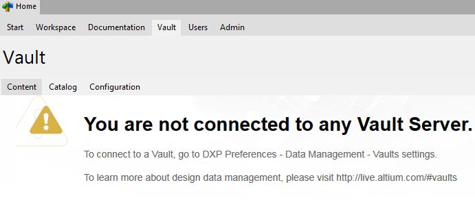
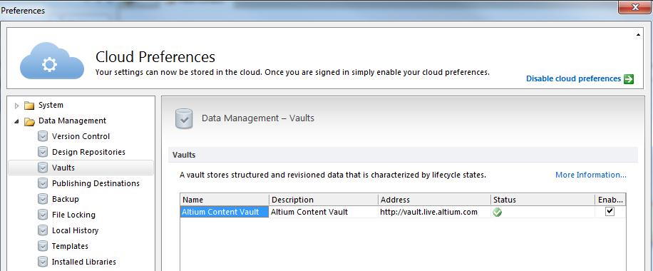
10 Connecting to the Altium Vault
11 Understanding Altium DXP (Design explorer): Unified platform Collaborative environment (corporate tool): Multiple users, some with dedicated tasks Design team incremental changes day-by-day Built-in version control (SVN subversion or CVS concurrent versions system Design repositories / Vaults (accessible by multiple users with different credentials Cloud oriented: Save preferences (forum, design content, blog)

12 Altium Design Environment

13 Recommended basic panels Projects Libraries Messages

14 Understanding Altium (Basics for the single user) Use Keyboard shortcuts <Shift + F1> while running a command <Esc> or Right Click to exit a command Save documents to see some changes take effect
15 Understanding Altium (Basics for the single user) Projects (project panel, active project) Workspace Panels (system-wide, editor-specific) Editors: Schematic Symbol editor PCB layout Footprint editor CAM files (CAMtastic panel) Components and Libraries
16 Altium Projects Project: collection of design documents 1 Project = 1 implementation It stores links to all source documents relative reference: same drive absolute reference: different drive It creates links to all output documents Saves project options Create a PCB_Project, Save as: new name (does not move the file creates a copy) The active project is highlighted Add/Remove documents to/from a project
17 Altium Projects: types PCB Project (*.PrjPcb) Schematic, libraries, PCB layout FPGA Project (*.PrjFpg) Embedded Project (*.PrjEmb) Core Project (*.PrjCor) Integrated Library (*.LibPkg) & (*.IntLib) Scritpt Project (*.PrjScr)
18 Component, Model and Library Concepts Domains = Different phases of design Schematic capture PCB layout (2D / 3D) SPICE simulation Signal integrity analysis Different component representations A unified component is a container with links to all domain models + parametric information


19 Component, Model and Library Concepts Component representations: Schematic symbol PCB footprint SPICE model definitions Signal integrity description 3D graphical description

20 Component, Model and Library Concepts The built-in capability to create component visual representations, assign parameters, and create links between representations is very sophisticated
21 Libraries = collection of components Collection of components, models or both Model Libraries (*.MDL, *.CKT, *.PCBLib) Simulation models are one file per model Schematic Libraries (*SchLib) Symbol and a link to a model library Integrated Libraries (*.IntLib) Symbol, footprint and other models are compiled into a single portable file

22 Project: part of and available only to the active project and its documents You have to keep track of where these are if you move the project files Installed: All installed libraries. Components are available to all open projects and list is persistent across design sessions Search Path: Additional Libraries accessible via a search path and subfolders The search paths are valid for the active project

23 Libraries Panel: All libraries available to the active project Project + Installed + Search Path When placing component: <spacebar> to rotate <x> or <y> to flip <Tab> open properties dialog <L> for PCB footprints to flip component side To search across libraries: Search
24 Obtaining integrated libraries 1. Frozen libraries: from here you can install anywhere but it is a good idea to make a subfolder under: C:\Users\Public\Documents\Altium\AD14\Library or a cloud storage service if you use more than one PC 2. AltiumLive website: Resources / Design Content This is useful to preview component This downloads a.zip file for the complete library
25 Altium Vault Altium is a unified development environment Philosophy: Design for reuse Vault is a cloud repository of models, components, schematics, design modules etc. Vault-driven electronic design: release to and source from Vault Vault-based components not only include all models, but also include real-time supply chain information.


26 Learning how to use Altium Until recently: best training guides were for Altium 2009 (pdf lesson files organized in chapters) But DXP menus have changed since The same information is now updated in the Altium_wiki
27 Demo: Schematic entry and Simulation Miscellaneous Devices.IntLib NSC Amplifier.IntLib Amplitude =5V Frequency=50KHz C:\Users\Public\Documents\Altium\AD14\Library\Simulation\Simulation Sources.IntLib

28 Set simulation parameters
29 Wiring Tips Left-click or <Enter> to anchor the wire at the cursor position. <Backspace> ( ) to remove the last anchor point. <Spacebar> to toggle the direction of the corner. <Shift+Spacebar> to cycle through all possible corner modes. Right-click or <Esc> to exit wire placement mode. To graphically edit the shape of a wire, Click once to select it first, then Click and hold on a segment or vertex to move it. Whenever a wire crosses the connection point of a component, or is terminated on another wire, a junction will automatically be created. A wire that crosses the end of a pin will connect to that pin, even if you delete the junction. To move a placed component and drag connected wires with it, hold down the Ctrl key while moving the component, or select Move» Drag.

30 How to save results How to export a file Plugin for printing (Altium Live account)
31 About SPICE U.S DOD, CANCER Computer Analysis of Nonlinear Circuits Excluding Radiation Berkley, Simulation Program with Integrated Circuit Emphasis SPICE 1972 FORTRAN SPICE , SPICE 2G SPICE C, SPICE 3F SPICE (RF) Proprietary versions of SPICE SPICE-like simulators or Alphabet SPICE HSpice, XSPICE (Georgia Tech), PSPICE, etc
32 Altium and SPICE Altium Designer is compatible with: SPICE3f5 (Berkley SPICE) XSPICE (Georgia Tech) PSPICE (Micro/Sim/Orcad/Cadence) You may need to change the file extension to.mdl or.ckt SUBCKT /.ENDS Other models need to be manually converted!
33 SPICE Models and Subcircuits
34 SPICE Netlist Subcircuits, models + analysis command + graphical output settings Asterisks (*) = Comments, Plus (+) = Line continuation, Period (.) = Command Letters (A to Z) are used to represent elements, D= Diode, R = Resistor etc.
35 SPICE Syntax Reference (1/2)
36 SPICE Syntax Reference (2/2)
37 SPICE Unit multipliers
Altium I. (Circuit Design + Layout) ELEC391 Spring PCB Design support for ELEC391:
 ELEC391 Spring PCB Design support for ELEC391:") Altium I (Circuit Design + Layout) ELEC391 Spring 2018 PCB Design support for ELEC391: Altium 2016, 150 licenses Lecture talks: Jan 22 Altium I (Circuit Design + Layout) Mar 12 Guest Lecture PCB Production
Altium I (Circuit Design + Layout) ELEC391 Spring 2018 PCB Design support for ELEC391: Altium 2016, 150 licenses Lecture talks: Jan 22 Altium I (Circuit Design + Layout) Mar 12 Guest Lecture PCB Production
Building an Integrated Library
 Building an Integrated Library Old Content - visit altium.com/documentation Modified by on 6-Nov-2013 Integrated libraries combine schematic libraries with their related PCB footprints and/or SPICE and
To learn more about a command, dialog, object or panel, press F1 when the cursor is over that item.
 Published on Online Documentation for Altium Products (https://www.altium.com/documentation) 主页 > 从理念到制造 通过Altium Designer推动PCB设计 Altium技术文档新纪元 Modified by Jun Chu on Apr 26, 2018 Welcome to the world
Libraries. Modified by Jason Howie on Oct 24, Parent page: IntegratedLibrary Panels
 Libraries Modified by Jason Howie on Oct 24, 2017 Parent page: IntegratedLibrary Panels Use the Libraries panel to access components in libraries currently available in SOLIDWORKS PCB. Summary The Libraries
Defining & Running Circuit Simulation Analyses
 Defining & Running Circuit Simulation Analyses Summary Tutorial TU0106 (v1.6) April 20, 2008 This tutorial looks at creating a schematic of an analog filter design that is set up for circuit simulation.
From Idea to Manufacture - Driving a PCB Design through SOLIDWORKS PCB
 From Idea to Manufacture - Driving a PCB Design through SOLIDWORKS PCB Modified by Jason Howie on 24-Oct-2017 Welcome to the world of electronic product development in Altium's world-class electronic design
From Idea to Manufacture - Driving a PCB Design through CircuitStudio
 From Idea to Manufacture - Driving a PCB Design through CircuitStudio Modified by Susan Riege on 13-Sep-2018 Welcome to the world of electronic product development in Altium's world-class electronic design
Component, Model and Library Concepts
 Component, Model and Library Concepts Old Content - visit altium.com/documentation Modified by Susan Riege on 6-Aug-2016 Related Resources Net Ties and How to Use Them (PDF) This article explains Altium
Schematic Editing Essentials
 Summary Application Note AP0109 (v2.0) March 24, 2005 This application note looks at the placement and editing of schematic objects in Altium Designer. This application note provides a general overview
Linking a Simulation Model to a Schematic Component. Contents
 Linking a Simulation Model to a Schematic Component Contents Model Conversion Creating the Schematic Component Adding the Link Configuring the Link Specifying Model Type Linking to a SPICE 3f5 Model The
Moving to Altium Designer From P-CAD
 Summary Application Note AP0130 (v3.0) September 10, 2008 This application note highlights the key differences you need to be aware of when moving from P-CAD to Altium Designer. It will help you ramp up
Linking a Simulation Model to a Schematic Component
 Linking a Simulation Model to a Schematic Component Old Content - visit altium.com/documentation Modified by on 13-Sep-2017 Altium Designer provides a powerful mixed-signal circuit simulator, enabling
Moving to Altium Designer From P-CAD. Contents
 Moving to Altium Designer From P-CAD Contents File Translation Translation Overview Using the Import Wizard for P-CAD Files Working with Documents The Schematic Symbol Is the Component... P-CAD Components
Component Management in SOLIDWORKS PCB
 Component Management in SOLIDWORKS PCB Modified by Jason Howie on Oct 24, 2017 Parent page: Exploring SOLIDWORKS PCB A component is the general name given to a part that can be placed into an electronic
Editing Multiple Objects. Contents
 Editing Multiple Objects Contents Selecting Multiple Objects Inspecting the Objects Editing the Objects Editing Group Objects Step 1. Selecting the Capacitors Step 2. Changing the Comment String Step 3.
Tutorial - Getting Started with PCB Design
 Tutorial - Getting Started with PCB Design Old Content - visit altium.com/documentation Modified by Phil Loughhead on 3-Aug-2016 Welcome to the world of electronic product development environment in Altium
A Bus is a polyline object that is used, in conjunction with other objects, to define the connection of multiple nets.
 Bus Old Content - visit altium.com/documentation Modified by Admin on Sep 13, 2017 Parent page: Objects A Bus is a polyline object that is used, in conjunction with other objects, to define the connection
Published on Online Documentation for Altium Products (
 Published on Online Documentation for Altium Products (https://www.altium.com/documentation) Home > Understanding Models, Components and Libraries Using Altium Documentation Modified by Phil Loughhead on
Getting Started with PCB Design
 Getting Started with PCB Design Summary Tutorial TU0117 (v1.2) April 13, 2005 This introductory tutorial is designed to give you an overview of how to create a schematic, update the design information
Tutorial : First board in CircuitMaker.
 Tutorial : First board in CircuitMaker. Objectives 1. Create a new project in CircuitMaker. 2. Design electronic circuit in CircuitMaker schematic editor. 3. Design a pcb board for your circuit in CircuitMaker
Schematic Libraries, Models and Integrated Libraries
 Published on Online Documentation for Altium Products (https://www.altium.com/documentation) Главная > A Look at Creating Library Components Using Altium Documentation Modified by Jason Howie on Apr 11,
Introduction to PSpice
 Introduction to PSpice Simulation Software 1 The Origins of SPICE In the 1960 s, simulation software begins CANCER Computer Analysis of Nonlinear Circuits, Excluding Radiation Developed at the University
Altium Designer Panels. Contents
 Altium Designer s Contents CAM Editor Design Compiler s Embedded s Instrument-Rack s Other Instrument s PCB Editor and PCB Library Editor s Schematic Editor and Schematic Library Editor s Scripting s Signal
Using the SVN Database Library Conversion Wizard
 Published on Online Documentation for Altium Products (https://www.altium.com/documentation) 主页 > SVN Database Library Conversion Wizard Using Altium Documentation Modified by Rob Evans on Jun 19, 2017
Published on Online Documentation for Altium Products (https://www.altium.com/documentation)
") Published on Online Documentation for Altium Products (https://www.altium.com/documentation) Home > Sheet Symbol Using Altium Documentation Modified by Susan Riege on Apr 11, 2017 Parent page: Schematic
Published on Online Documentation for Altium Products (https://www.altium.com/documentation) Home > Sheet Symbol Using Altium Documentation Modified by Susan Riege on Apr 11, 2017 Parent page: Schematic
Moving to Altium Designer from Pads Logic and PADS Layout
 Moving to Altium Designer from Pads Logic and PADS Layout Old Content - visit altium.com/documentation Modified by on 13-Sep-2017 Translating complete PADS Logic and PADS Layout designs, including PCB,
Moving to Altium Designer from Protel 99 SE. Contents
 Moving to Altium Designer from Protel 99 SE Contents Design Database Become a Design Workspace & Projects Importing a 99 SE Design Database Creating the Altium Designer Project(s) Manually Adding and Removing
Probes are available for placement in the Schematic Editor only, by choosing Place» Directives» Instrument Probe [P, V, I] from the main menus.
![Probes are available for placement in the Schematic Editor only, by choosing Place» Directives» Instrument Probe [P, V, I] from the main menus.](/thumbs/88/116292734.jpg "Probes are available for placement in the Schematic Editor only, by choosing Place» Directives» Instrument Probe [P, V, I] from the main menus.") Instrument Probe Old Content - visit altium.com/documentation Modified by Admin on Nov 18, 2013 Parent Page: Objects An Instrument Probe. Summary An instrument probe is a design directive. It instructs
Instrument Probe Old Content - visit altium.com/documentation Modified by Admin on Nov 18, 2013 Parent Page: Objects An Instrument Probe. Summary An instrument probe is a design directive. It instructs
NEW USER S GUIDE TO DEFINING A LIBRARY METHODOLOGY
 When choosing a PCB library methodology, there is no one universal solution for all users. While some small business users may require only a bare essential yet the extremely flexible representation of
Design capture, simulation and layout - an introduction Tutorial
 Design capture, simulation and layout - an introduction Tutorial A step-by-step introduction to Altium s complete board-level design system 1 Software, documentation and related materials: Copyright 2002
Shortcut Keys. Access Choose Document to Open dialog. Cycle through open documents (to the left) Hide/display all floating panels
 Hide/display all floating panels") Summary Guide GU0104 (v1.9) February 11, 2008 This guide provides a list of shortcut keys available for use within Altium Designer, ranging from those used at the environment level, through to those associated
Summary Guide GU0104 (v1.9) February 11, 2008 This guide provides a list of shortcut keys available for use within Altium Designer, ranging from those used at the environment level, through to those associated
Lesson 18: Creating a Hierarchical Block
 Lesson 18: Creating a Hierarchical Block Lesson Objectives After you complete this lesson you will be able to: Create hierarchical blocks Copying Schematics between Projects You can copy and paste between
Welcome to the Altium Designer Environment
 Welcome to the Altium Designer Environment Summary Guide GU0112 (v1.0) April 29, 2005 Altium Designer brings a complete electronic product development environment to your PC s Desktop, providing multi-document
Lesson 1: Getting Started with OrCAD Capture
 1 Lesson 1: Getting Started with OrCAD Capture Lesson Objectives Discuss design flow using OrCAD Capture Learn how to start OrCAD Capture The OrCAD Capture Start Page Open an existing Project Explore the
TUTORIAL SESSION Technical Group Hoda Najafi & Sunita Bhide
 TUTORIAL SESSION 2014 Technical Group Hoda Najafi & Sunita Bhide SETUP PROCEDURE Start the Altium Designer Software. (Figure 1) Ensure that the Files and Projects tabs are located somewhere on the screen.
Published on Online Documentation for Altium Products (
 Published on Online Documentation for Altium Products (https://www.altium.com/documentation) Home > Coverlay Polygon Using Altium Documentation Modified by Phil Loughhead on Oct 24, 2018 Parent Page: PCB
Baseline dimension objects are available for placement in the PCB Editor only, by clicking Home
 Baseline Dimension Modified by Jason Howie on 24-Oct-2014 Parent page: Dimension A placed Baseline Dimension. Summary A baseline dimension is a group design object. It allows for the dimensioning of a
Published on Online Documentation for Altium Products (
 Published on Online Documentation for Altium Products (https://www.altium.com/documentation) Home > SnapSTEPModel Using Altium Documentation Modified by Jason Howie on Apr 11, 2017 Parent page: PCB Commands
Collaborate, Compare and Merge Panel. Contents
 Collaborate, Compare and Merge Panel Contents Panel Access Terminology and Status Messages Actions section Work in Progress Regions Version Control Status Difference Map section Cell Differences See Also
Database Library Migration Tools. Contents
 Database Library Migration Tools Contents Creating a Database Library from an Integrated Library Converting to a DBLib Specifying the Target Database Specifying the Target Database Library Choosing the
Folder Type. Parent page: Managed Domain Models
 Published on Online Documentation for Altium Products (https://www.altium.com/documentation) 主页 > Managed Simulation Models Using Altium Documentation Modified by Jason Howie on Jun 22, 2018 Parent page:
Switch between open apps Close the active item, or exit the active app
 Ctrl + X Ctrl + C (or Ctrl + Insert) Ctrl + V (or Shift + Insert) Ctrl + Z Alt + Tab Alt + F4 L D F2 F3 F4 F5 F6 F10 Alt + F8 Alt + Esc Alt + underlined letter Alt + Enter Alt + Spacebar Alt + Left arrow
OrCad & Spice Tutorial By, Ronak Gandhi Syracuse University
 OrCad & Spice Tutorial By, Ronak Gandhi Syracuse University Brief overview: OrCad is a suite of tools from Cadence for the design and layout of circuit design and PCB design. We are currently using version
Moving to Altium Designer from Protel 99 SE
 Moving to Altium Designer from Protel 99 SE Summary This article outlines the process you go through to transfer a Protel 99 SE design into the Altium Designer environment. Protel 99 SE uses the design
3D Body. Summary. Modified by Admin on Sep 13, Parent page: Objects
 3D Body Old Content - visit altium.com/documentation Modified by Admin on Sep 13, 2017 Parent page: Objects A sphere, a cylinder and 4 extruded rectangles have been used to create the 3D body for an LED.
Moving to Altium Designer from PADS Layout and OrCAD capture. Contents
 Moving to Altium Designer from PADS Layout and OrCAD capture Contents Getting Started - Transferring Your PADS Layout Designs Using the Import Wizard for PADS Layout Files Layer Mapping for PADS PCB ASCII
Radial Diameter Dimension. Contents
 Radial Diameter Dimension Contents Description Availability Placement Editing via an Associated Properties Dialog Editing via the PCB Inspector Panel Editing via the PCB List Panel Graphical Editing Notes
Exercise 1. Section 2. Working in Capture
 Exercise 1 Section 1. Introduction In this exercise, a simple circuit will be drawn in OrCAD Capture and a netlist file will be generated. Then the netlist file will be read into OrCAD Layout. In Layout,
Adding a Simulation Model to a Component Definition
 Adding a Simulation Model to a Component Definition Old Content - see latest equivalent Modified by on 13-Sep-2017 Parent article: Releasing a Component Definition to a Vault On the design side, each design
1 Ctrl + X Cut the selected item. 2 Ctrl + C (or Ctrl + Insert) Copy the selected item. 3 Ctrl + V (or Shift + Insert) Paste the selected item
 Copy the selected item. 3 Ctrl + V (or Shift + Insert) Paste the selected item") Tips and Tricks Recorder Actions Library XPath Syntax Hotkeys Windows Hotkeys General Keyboard Shortcuts Windows Explorer Shortcuts Command Prompt Shortcuts Dialog Box Keyboard Shortcuts Excel Hotkeys
Tips and Tricks Recorder Actions Library XPath Syntax Hotkeys Windows Hotkeys General Keyboard Shortcuts Windows Explorer Shortcuts Command Prompt Shortcuts Dialog Box Keyboard Shortcuts Excel Hotkeys
Component. Modified by Jason Howie on Feb 13, Parent page: PCB Dialogs. Other Related Resources Component (Object) The Component Dialog.
 The Component Dialog.") Component Modified by Jason Howie on Feb 13, 2015 Other Related Resources Component (Object) Parent page: PCB Dialogs The Component Dialog. Summary The Component dialog is used to edit the properties of
Component Modified by Jason Howie on Feb 13, 2015 Other Related Resources Component (Object) Parent page: PCB Dialogs The Component Dialog. Summary The Component dialog is used to edit the properties of
The three sections in this manual include training notes and related exercises for the following one-day training sessions:
 Training Manual DXP2004 Training Welcome to the DXP 2004 training manual. The three sections in this manual include training notes and related exercises for the following one-day training sessions: Design
Altium Designer Functional Areas
 Altium Designer Functional Areas Why Data Management The Idea behind Altium Designer Copyright 2013 Altium Limited Functional units of AD JK, v 2.3 2 ONE Tool for each Electronic Design Engineer What exactly
Generating a Custom Bill of Materials
 Generating a Custom Bill of Materials Old Content - visit altium.com/documentation Modified by on 6-Nov-2013 This tutorial describes how to use the Report Manager to set up a Bill of Materials (BOM) report.
Baseline dimension objects are available for placement in the PCB Editor only. Use one of the following methods to access a placement command:
 Baseline Dimension Old Content - visit altium.com/documentation Modified by on 19-Nov-2013 Parent page: Objects A placed Baseline Dimension. Summary A baseline dimension is a group design object. It allows
Moving to Altium Designer From OrCAD. Contents
 Moving to Altium Designer From OrCAD Contents File Translation OrCAD Capture 10.x *.DSN Files and the Unrecognized Project File Version Error Default Layer Mapping for PCB Using the Import Wizard for OrCAD
Getting Started with FPGA Design
 Getting Started with FPGA Design Summary Tutorial TU0116 (v1.3) April 13, 2005 This tutorial gives an overview of how to create an FPGA design. It outlines how to create a schematic and then compile, synthesize,
Published on Online Documentation for Altium Products (
 Published on Online Documentation for Altium Products (https://www.altium.com/documentation) Главная > Working with the Explorer Panel - Feature How-Tos Using Altium Documentation Modified by Jason Howie
Using the Import Wizard
 Published on Online Documentation for Altium Products (https://www.altium.com/documentation) 主页 > Import Wizard Using Altium Documentation Modified by Phil Loughhead on Jun 18, 2017 The Import Wizard will
Working with Version-Controlled Database Libraries. Contents
 Working with Version-Controlled Database Libraries Contents Librarian or Designer? Working as a Librarian The Source Control Repository Using the Library Splitter Wizard Creating the SVN Database Library
Altium Designer Viewer. Contents
 Altium Designer Viewer Contents What You can do Key Features at-a-glance Supported Output Generation Viewer Environment Viewing Schematic Documents Viewing PCB Documents Searching Live Supplier Data Using
Part. Summary. Modified by Susan Riege on Aug 5, Parent page: Objects
 Part Old Content - visit altium.com/documentation Modified by Susan Riege on Aug 5, 2016 Parent page: Objects Related Resources Net Ties and How to Use Them (PDF) The Part represents the actual physical
This document provides detailed information on placing components from a database using Altium Designer's SVN Database Library feature.
 Old Content - visit altium.com/documentation Mod ifi ed by on 13- Sep -20 17 This document provides detailed information on placing components from a database using Altium Designer's SVN Database Library
Published on Online Documentation for Altium Products (
 Published on Online Documentation for Altium Products (https://www.altium.com/documentation) Home > Managed Simulation Models Using Altium Documentation Modified by Jason Howie on Jun 22, 2018 Parent page:
How to Get Started. Figure 3
 Tutorial PSpice How to Get Started To start a simulation, begin by going to the Start button on the Windows toolbar, then select Engineering Tools, then OrCAD Demo. From now on the document menu selection
Comments. Summary. Modified by Rob Evans on Jun 10, Parent page: Workspace Manager Panels
 Comments Modified by Rob Evans on Jun 10, 2015 Parent page: Workspace Manager Panels The Comments panel showing a collection of user comments for the currently active project. Summary The Comments panel
Schematic Symbol Generation Tool
 Schematic Symbol Generation Tool Old Content - visit altium.com/documentation Modified by Rob Evans on May 4, 2015 The task of creating a component library symbol and its pin data has become an increasingly
A Tour of the Scripting System. Contents
 A Tour of the Scripting System Contents Features of the Scripting System Script Projects and Scripts Scripting Editor Scripting Panels Scripting Debugger Several Scripting Languages Application Programming
OutputJob Editor Reference
 OutputJob Editor Reference Summary This reference provides information on the OutputJob Editor which is used to configure various output types including Assembly Outputs, BOMs, Gerber, NC Drill, Netlists,
Complete Tutorial (Includes Schematic & Layout)
") Complete Tutorial (Includes Schematic & Layout) Download 1. Go to the "Download Free PCB123 Software" button or click here. 2. Enter your e-mail address and for your primary interest in the product. (Your
Complete Tutorial (Includes Schematic & Layout) Download 1. Go to the "Download Free PCB123 Software" button or click here. 2. Enter your e-mail address and for your primary interest in the product. (Your
Releasing a Simulation Model to a Vault
 Releasing a Simulation Model to a Vault Old Content - see latest equivalent Modified by Jason Howie on May 31, 2017 Parent article: Vault-Based Domain Models From a designer's perspective, a vault-based
Storage Manager. Summary. Panel access. Modified by on 10-Jan-2014
 Storage Manager Old Content - visit altium.com/documentation Modified by on 10-Jan-2014 Related panel: Differences Panel Related documents: Version Control and Altium Designer Version Control Terminology
Parent page: PCB Panel
 Published on Online Documentation for Altium Products (https://www.altium.com/documentation) 主页 > PCB Library Using Altium Documentation Modified by Annika Krilov on Apr 11, 2017 Parent page: PCB Panel
Using Components Directly from Your Company Database
 Using Components Directly from Your Company Database Old Content - visit altium.com/documentation Modified by Phil Loughhead on 18-May-2016 This document provides detailed information on using components
Published on Online Documentation for Altium Products (
 Published on Online Documentation for Altium Products (https://www.altium.com/documentation) Home > Creating the PCB Footprint Using Altium Documentation Modified by Annika Krilov on Apr 11, 2017 Concept
Cycle through three routing modes (ignore, avoid or push obstacle) Toggle electrical grid on/off
 Toggle electrical grid on/off") PCB Editor Shortcuts Old Content - visit altium.com/documentation Modified by on 13-Sep-2017 Parent article: Shortcut Keys PCB Editor Shortcuts + E + B + PAGE UP + PAGE DOWN Cycle through three routing
PCB Editor Shortcuts Old Content - visit altium.com/documentation Modified by on 13-Sep-2017 Parent article: Shortcut Keys PCB Editor Shortcuts + E + B + PAGE UP + PAGE DOWN Cycle through three routing
Polygon Pours and Copper Regions. Fills and Solid Regions. Modified by Admin on Nov 18, 2013
 Polygon Pours and Copper Regions Old Content - visit altium.com/documentation Modified by Admin on Nov 18, 2013 A common requirement on a printed circuit board is large areas of copper. It could be a hatched
Tutorial on Quartus II Introduction Using Verilog Code
 Tutorial on Quartus II Introduction Using Verilog Code (Version 15) 1 Introduction This tutorial presents an introduction to the Quartus II CAD system. It gives a general overview of a typical CAD flow
Schematic/Design Creation
 Schematic/Design Creation D A T A S H E E T MAJOR BENEFITS: Xpedition xdx Designer is a complete solution for design creation, definition, and reuse. Overview Creating competitive products is about more
Lesson 17: Building a Hierarchical Design
 Lesson 17: Building a Hierarchical Design Lesson Objectives After you complete this lesson you will be able to: Explore the structure of a hierarchical design Editing the Training Root Schematic Making
Published on Online Documentation for Altium Products (
 Published on Online Documentation for Altium Products (https://www.altium.com/documentation) Home > Storage Manager Using Altium Documentation Modified by Jason Howie on Jun 16, 2017 Parent page: System
TUTORIAL How to Use the SPICE Module
 TUTORIAL How to Use the SPICE Module February 2018 1 1. Overview The SPICE Module is an add-on option in PSIM. Powered by CoolSPICE developed by CoolCAD Electronics LLC., the SPICE Module provides a SPICE
Interactively Routing a Net
 Interactively Routing a Net Old Content - visit altium.com/documentation Modified by on 18-Nov-2013 Interactive Routing is more than placing down track objects to join the dots (pads). Altium Designer
One possible window configuration preferences for debug cycles
 NEW USER S TUTORIAL Welcome to ICAP/4, Intusoft s suite of analog and mixed-signal simulation products. There is also a New User s Tutorial 2 as follow-on to this tutorial for non-icap/4rx products. Let
Introduction Creating a Project Footprint Design
 EEC 134 Application Note Introduction to PCB Design Cameron Vossoughi Introduction Being fluent in PCB design is essential for electrical engineers regardless of their discipline focus. This application
Ansys Designer RF Training Lecture 2: Introduction to the Designer GUI
 Ansys Designer RF Solutions for RF/Microwave Component and System Design 7. 0 Release Ansys Designer RF Training Lecture 2: Introduction to the Designer GUI Ansoft Designer Desktop Menu bar Toolbars Schematic
Revision: February 27, E Main Suite D Pullman, WA (509) Voice and Fax
 Voice and Fax") Xilinx ISE WebPACK Schematic Capture Tutorial Revision: February 27, 2010 215 E Main Suite D Pullman, WA 99163 (509) 334 6306 Voice and Fax Overview This tutorial provides instruction for using the Xilinx
Xilinx ISE WebPACK Schematic Capture Tutorial Revision: February 27, 2010 215 E Main Suite D Pullman, WA 99163 (509) 334 6306 Voice and Fax Overview This tutorial provides instruction for using the Xilinx
Lab 1: Analysis of DC and AC circuits using PSPICE
 Lab 1: Analysis of DC and AC circuits using PSPICE 1. Objectives. 1) Familiarize yourself with PSPICE simulation software environment. 2) Obtain confidence in performing DC and AC circuit simulation. 2.
Drill Table. Summary. Modified by Phil Loughhead on 16-Jun Parent page: PCB Dialogs
 Drill Table Old Content - visit altium.com/documentation Modified by Phil Loughhead on 16-Jun-2015 Parent page: PCB Dialogs The Drill Table Dialog. Summary A standard element required for manufacture of
PSpice with Orcad 10
 PSpice with Orcad 10 1. Creating Circuits Using PSpice Tutorial 2. AC Analysis 3. Step Response 4. Dependent Sources 5. Variable Phase VSin Source Page 1 of 29 Creating Circuits using PSpice Start Orcad
CadSoft EAGLE Importer
 CadSoft EAGLE Importer Old Content - visit altium.com/documentation Modified by on 31-Jan-2014 Related Videos EAGLE Importer Not all design work is done in Altium Designer. If you are new to Altium Designer,
Published on Online Documentation for Altium Products (
 Published on Online Documentation for Altium Products (https://www.altium.com/documentation) Главная > Working with the Vaults Panel - Feature How-Tos Using Altium Documentation Modified by Jason Howie
Component Management in CircuitMaker
 Component Management in CircuitMaker Modified by Rob Evans on 14-Oct-2015 Related pages Driving a PCB Design through CircuitMaker Project Management Parent page: Exploring CircuitMaker A component is the
EE 210 Lab Assignment #2: Intro to PSPICE
 EE 210 Lab Assignment #2: Intro to PSPICE ITEMS REQUIRED None Non-formal Report due at the ASSIGNMENT beginning of the next lab no conclusion required Answers and results from all of the numbered, bolded
Defining Net Classes by Area on a Schematic. Creating a Net Class from a Blanket Directive. Modified by Admin on Sep 13, Blankets in Schematic
 Defining Net Classes by Area on a Schematic Old Content - visit altium.com/documentation Modified by Admin on Sep 13, 2017 Related Video Blankets in Schematic Altium Designer already allows you to create
A Walk Through...the Board Design Release Process. Contents
 A Walk Through...the Board Design Release Process Contents Design Project - Initial Preparation Create a New Design Repository Add Your Project to the Design Repository Connect to an Altium Vault Define
Copy of A Walk Through...the Board Design Release Process
 Copy of A Walk Through...the Board Design Release Process Language Japanese Contents Design Project - Initial Preparation Create a New Design Repository Add Your Project to the Design Repository Connect
PSpice Tutorial. Physics 160 Spring 2006
 PSpice Tutorial This is a tutorial designed to guide you through the simulation assignment included in the first homework set. You may either use the program as installed in the lab, or you may install
Pads are used to provide both mechanical mounting and electrical connections to the component pins.
 Pad Old Content - visit altium.com/documentation Modified by Jason Howie on 19-Aug-2015 Parent page: Objects Pads are used to provide both mechanical mounting and electrical connections to the component
Creating a Database Library from an Integrated Library
 Published on Online Documentation for Altium Products (https://www.altium.com/documentation) Home > Database Library Migration Tools Using Altium Documentation Modified by Jason Howie on Apr 11, 2017 Parent