Complete Tutorial (Includes Schematic & Layout)
|
|
|
- Gervais Harry Pitts
- 5 years ago
- Views:
Transcription
1 Complete Tutorial (Includes Schematic & Layout) Download 1. Go to the "Download Free PCB123 Software" button or click here. 2. Enter your address and for your primary interest in the product. (Your information is kept private.) 3. After you submit this information, we will send a link to your for you to download the free software. Typical download time is: 10-to-15 minutes for a modem >30 seconds for DSL or cable modem Want to know who else is using PCB123? Click here. Installing Software 1. Click on the software link in your and the downloading process will begin. 2. A dialog box will then ask you where you would like to install the software. 3. Go through the quick installing procedure, which includes a standard EULA (end user licensing agreement) 4. You are now ready to begin designing your printed circuit board!! PCB123 Testing Tutorial There are two applications included in our product that we will be using in our tutorial. PCB123Schematic: You can create an easy to read, one dimensional schematic diagram of a functional circuit and from this diagram a netlist can be generated. This netlist is basically a description of all the parts in your diagram and describes how these parts are connected to make your circuit. The netlist is useful for PCB123Layout to start with. PCB123Layout: You can layout and design physical characteristics of your schematic with PCB123Layout. Although you can design circuit boards without a schematic diagram, it is needed to run the batch routing routines in the PCB123Layout application. It is also a good idea to start with a schematic diagram to aid in the verification that all your circuits are connected properly on your final printed circuit board layout. If you see problems or omissions from this document please let us know ASAP support@pcb123.com
2 PCB123Schematic - "Creating the Schematic Drawing" This tutorial will show you how to design the schematic drawing in Figure 1. You can look at this sample file in the following directory: Examples/Decade.epc. Figure 1: Example Finished Tutorial Project: Analog-to-Digital Converter Interface Schematic Design Schematic Diagram: A schematic diagram is a visual representation of an electronic circuit. PCB123 Schematic is a computer-aided design environment used to help the user in the designing of an electronic circuit. This process, called schematic capture, is not just a simple drawing of a circuit. It provides information about the connectivity of all the parts that make up this circuit. This computer-based information is then used to create a netlist program. This netlist is then used in performing electrical design checks and to transfer the circuit connections and its component packages to the in the next step of the process of laying out the circuits as a printed circuit board (PCB). This process of capturing a design of an electronic circuit involves the placing and arranging of schematic symbols, which fully or partially represent the electronic components that will make up the circuit, and then placing connecting lines to describe the continuity of the circuit.
3 Connectivity of Schematic Objects Connectivity is the electrical links between objects in the schematic design area. Objects with electrical properties and their own functionalities are: Schematic symbols Wires Junctions Net labels Schematic symbol parts: A schematic symbol is a representation of an electronic component. These objects usually have multiple connection points or terminals that describe a pin location on the actual component. Each terminal has a pin number corresponding to the pin of the physical component and may have a label to describe this pin. A connection can be made to a terminal by drawing a wire to the terminal end or anywhere along its length. If a connection is made along its length a junction will be placed at the intersection. Note: There are also special schematic symbols that will let you easily connect a network to ground. Note: Hidden terminals are another way to show connectivity through a schematic symbol. This method connects hidden terminals to special net identifiers VCC, +v, -v, and gnd automatically through the design of the symbol part. Wire Object: Wires are the main object used to define connectivity in a diagram. They can be arranged end-to-end creating a path from terminal to terminal. The main connection points of a wire are at its ends, but connections can also be made anywhere along its length. Junctions are used at these intersections to show they are connected. Junctions: Junctions are used to show connectivity at intersections of wires or terminals. These are automatic. If a wire ends on another wire there will be a junction. If two wires cross but do not terminate at their intersection, there will not be a junction and therefore will not connect. Net labels: Net labels are used to assign net names to electrical nets. They show connectivity not by physically joining networks, but by assigning common net names to different networks on the schematic. The netlister will interpret these networks and combine them into one network.


4 Starting a new Schematic Diagram 1. Open up the PCB123 chematic application. Figure 2: Initial Sreen of the PCB123Schematic Application 2. Save the new diagram by clicking File Save As and name it 'TestTutorial.epc'. 3. Notice that the Title in the title block, located at the bottom right of the page frame, will also change to reflect new file name 'Title: TestTutorial.epc'. Figure 3: Title Block

5 4. You can edit the information in the title block by going to Settings Page Setup Schematic Page Setup. Figure 4: Changing Project Information When you are designing, the snap-to-grid is always on.

6 Inserting and Editing Schematic Parts There are 3 different ways of adding parts to your schematic diagram. Library Parts Dialog Using the Parts Bin Duplicating Existing Parts Library Parts Dialog 1. Select Edit Insert Object Library Part from the menu or click the button from the Edit toolbar to open the Library Parts dialog: Figure 5: Library Parts Dialogue 2. Select genxxx.con from the Library list. 3. Select then D74192 from the Part list. 4. Click the Load Part button. Position the cursor inside the drawing border. (Note: You may have to zoom out to see the drawing border with the title block in the lower right hand corner.) Left-click on the work area to place the part. (Note: By pressing the left-mouse button and holding it down you can drag the mouse to precisely place your part.) 5. Place these additional parts using this method: Quantity Library Part Name 4 GENXX.con D DEVICE Push_button

7 Using the Parts Bin Common and frequently used parts can be accessed quickly from the Parts Bin. To display the Parts Bin, click on the from the Main toolbar. Figure 6: Part Bin Dialog You will see a collection of 12 commonly used parts which can be modified to hold your favorite parts. To insert a part, simply select and drag the part onto your diagram. Using the Parts Bin method, insert the following parts (if you can t find the parts in the Parts Bin, look in the Library Parts dialog). Quantity Type Library Part Name 2 GND (ground) 1 resistor DEVICE resistor 1 LED DEVICE LED
. When you release the mouse, a copy of the part will appear at the location of the cursor.")
8 Duplicating Existing Parts The Duplicate Existing Parts method consists of holding down the SHIFT key while holding down the left-mouse button and dragging a part (you have to be in Select Mode, which takes you out of the other modes). When you release the mouse, a copy of the part will appear at the location of the cursor. Now use the Duplicate Existing Parts method to create duplicates from existing items on the diagram: Quantity Type Library Part Name 5 resistor DEVICE resistor 3 LED DEVICE LED Assigning Unique Reference Numbers Once all parts are placed in the design, all reference designators for the resistors and LED s need to be reset (renumbered). 1. To reset the reference numbers click Design Reset Ref Designators...and a dialog box will appear. Figure 7: Reset Reference Numbers 2. Clicking OK will renumber all reference numbers starting with To reset only one type of item, enter its initial in the Enter Type (a-z) field. Example: to reset only resistors, type R, then OK.

9 Arrange Objects to Match Example Arrange all the objects in the diagram to match the example in Figure 1. Refer to the section Editing Objects for help in arranging them. (The LED s were mirrored to achieve their appearance.) Figure 8: Objects Before Schematic Wiring Editing Objects Select Mode: To select an object, you must first be in Select mode, which is the default mode. Select objects by clicking on the icon in the toolbar, or use the Escape-key to get to Select mode, then left-mouse clicking on the object. You can select multiple objects by holding down the control-key while selecting objects. Deleting: To delete a part, go into Select mode, select the object and hit the delete key. Escape-key: To escape from other modes, hit the Escape-key. Mirroring: The button flips the object horizontally on the diagram. Moving: To move parts once they have been placed, simply select the part by holding down the left-mouse button and then drag to a new position. Rotation: You can rotate most objects as needed with the button. If parts of the object do not rotate correctly, try mirroring. Rubberband Mode: When Rubberband Mode is enabled, connectivity of the schematic is maintained when parts or wire ends are moved. Wires will stretch to maintain their connection to terminals of part when they are dragged to new positions in the drawing area.
10 Wiring the Schematic To wire the schematic you will need to make simple terminal-to-terminal connections using the wire object. Each connection is a series of wire objects, segments, that are independently selectable and editable. Note: A general rule is to stick to only horizontal and vertical wire layouts. The following steps describe how to insert a wire segment. 1. Select Edit Insert Object Wire from the menu or from the Edit toolbar. 2. Position the cursor where you want the wire segment to begin. 3. Push and hold down the left-mouse button. 4. Drag the mouse to the position where you want to end the wire segment. 5. Release the left-mouse button. Wiring Information Junctions: automatically inserted by the program where a wire segment is started or ended in the middle of another wire (see Figure 9). A junction will not be placed if: A: two wires cross each other without terminating at the intersection C: two wires connect at their ends only, such as turning a corner A junction will be placed if: B: there is an accidental termination in one of the wires, at an intersection, but it is hard to see unless you click on the wire. D: there is a termination at an intersection. Figure 9: Junction Examples and Troubleshooting Segments: segments can be a selectable part of a connection. Connections: Connections are a collection of segments between objects.

11 Adding/Modifying Net Names The netlister will assign each net a unique net name. However, you can manually name nets so that their functions within the associated circuit are easier to understand or remember over long periods of time. For example, you may want to call a clock wire "CLOCK", and a set of memory address lines "A0"-"A11". If you assign two separate nodes to the same net name, they will effectively be connected electrically in the netlist. In our schematic diagram there are seven nets that have been manually assigned. For this design, the only net that is required by the netlist to be assigned is the VCC. (See Note below) Use the Text object to add net names to the network. You should be in snap-to-grid mode, with the cross-hairs cursor showing. Place the cursor on any vertical, or horizontal line, or device terminal, which belongs to the net. Click, and type the name; push the "Esc" key to end the name. Follow these steps to assign new net names: 1. Go to the menu, and select Edit Insert Object Text or click from the Edit toolbar. 2. Locate the cursor on one of the wire segments of the net to be assigned and left-click your mouse. 3. Enter the new net name. 4. In the project, you need to enter VCC and Reset in the locations similar to Figure 10. Editing the VCC in this design will effect 3 locations. Figure 10: Entering Net Names NOTE: VCC is a standard net name, which refers to the digital IC +5 volt power. Although these terminal pins are not displayed in the schematic for each IC component, they are taken in account by the netlister. When the netlist extracts the netlist it connects any terminals connected to a net named VCC to the IC +5 volt power. The same is true for signals attached to the ground symbol (GND part). They are automatically connected to the IC ground terminals by the netlister.
 Caution: Do not end the net name with a dash character -.")

12 It is not necessary to have net names on all nets in a schematic; the netlister will add default names. The Text object location must be within five screen pixels of the wire being assigned. Net names are limited to 8 or less characters and cannot contain the space character. (For example, do not use CLK IN, instead use CLK_IN) Caution: Do not end the net name with a dash character -. format when it is read into the Layout application. It will cause problems with the netlist Finishing the Schematic All essential parts have been done to generate a netlist at this point. To save the schematic diagram select File Save from the menu. Convert To Layout Creating a Netlist and Auto Place Parts While still in PCB123Schematic you can go to the PCB123Layout application in one simple step by going to the menu and selecting Design Convert to Layout. You will see the following dialog: 1. Click Convert. 2. Click Yes 3. Click OK. 4. A new netlist will be generated in PCB123Layout. 5. The PCB123Layout application launches 6. All components in your design will be placed in Layout application.


13 7. A Layout information dialog will be displayed, Click Done 8. You will see this report or you will see an errors report. 9. This is your circuit in PCB123Layout, save it, then proceed.

14 Board Configuration To edit the Board Configuration: 1. Go to the Standard Menu 2. Select Design Board Configuration The Board Configuration dialog will be displayed. Select the board configuration you need, then click OK. Figure 11: Configuring Your Board
15 PCB123Layout - "Laying Out Your Board Design" Before you continue, you may want to edit your grid s visibility, which can aid you when it comes time to route your board. Figure 12: Modifying the Grid

16 Rearranging the Components The goal in rearranging components on the board is to move and orient the components in such a way as to insure the shortest possible routing of each net. 1. Make the Ratsnest invisible to make it easier to rearrange components. Since we are getting ready to place the board, we don t care about selecting text or doing any routing. 2. Turn these off by toggling the button and the button on the right-hand toolbar. Figure 13: Making the Ratsnest Invisible 1. As a general rule, you should place the component with the most connections in the center of the board. 2. Next, select the component with the next greatest connections and place it. You may have to rotate the component to get the right fit. Continue this process until all components are placed.

17 Editing the Board Outline The Board outline describes the general shape of your board. Board Outlines can be generated, or modified with these three tools: Polygon, Arc and Circle. To edit the shape of your board, doubleclick anywhere on the board outline, and drag it to the desired position. re 14: Rearranged Components and Board Outline Figu Route the Board Routing is the process of determining the path of routes that electrically connect components together. In our tutorial these connections are determined by the netlist generated by the schematic drawing supplied by the tutorial. By displaying the Ratsnest you can view these connections. Manual Routing vs. Autorouting The process of manually routing connections is to route the path of each connection one by one. These paths may go from one layer to another through vias. The goal here is to route all connections required by the netlist using the shortest path possible, while using a minimal amount of vias. Depending on your design this could be a very time consuming process. Fortunately this process can be made shorter and easier by using the integrated autorouter. The autorouter automatically routes all connections in the netlist. Autorouting This section demonstrates autorouting the board, or creating connections between components the easy way. 1. First, press the G key on your keyboard to invoke the Grid dialog. Enter a value of to establish your routing grid. 2. Go to the menu and select Design Autoroute and watch it start generating routes.
18 Figure 15: Autorouting Your Routes At the end of autorouting, if there are any connections the autorouter was not able to route they can be routed manually. To do this you may have to move traces and vias. The following are some common operations for inserting and modifying routes and vias.


19 Manual Routing As you mouseover the route, the cursor will dynamically change, and the route will highlight. Figure 16: Cursor Modes: Routing Mode Click on the route to re-arrange it. Figure 17: Cursor Modes: Re-Route Mode A spacing violation is when you drag a route too close to another one. Figure 18: Cursor Modes: Spacing Violation Mode

20 Manual Routing Tips Move corners: Just click on a corner of an object and drag it to where you want. You can fold consecutive corners over each other to optimize segments of routes away, giving the required clearance around an object. Move segment: Press the left-mouse button down and drag a segment to where you want it. Release the left-mouse button to drop the segment. Reroute segment: By single-clicking on the middle ¾ of a segment, you can dynamically ripup and reroute that segment. The benefits of this operation will soon become apparent as it lets you dynamically create in free form mode, including adding vias by simply changing layers as you go. A via is always inserted at the last corner clicked, not necessarily under the cursor. Rerouting also allows you to walk a route backwards, removing segments as you go. It is a very quick way to edit and modify routing. Routing: clicking on an unrouted (ratline, connection, airline, etc.) you simply create a connection by clicking corners. If you change layers in the midst of creating a connection, using the Z-key, a via (a connection between layers) will be inserted at the last corner made. Quick-Complete: Doubleclicking on a board outline or route will cause it to complete the connection, or complete the board enclosure. Segments: Segments snap to 45 degree increments unless you hold down the Ctrl-key. The Ctrl-key is an override and will allow you to route at any angle as long as it is held down. Changing Pad/ Hole Sizes of a Placed Part You may need to change the pad and/ or hole sizes of parts placed in your design. In our example design we will change the pad and hole sizes for all the resistors. 1. Select R1. 2. Right-click on R1 to bring up the Properties dialog. 3. Click the Pins tab. 4. Select the Pad shape: Round 5. Set the Pad Width and Pad Height to:.060", and the Drill size to.040"

21 Changing Trace Widths of VCC and Ground Next, we will change the trace widths of our VCC and Ground nets. Follow these steps: 1. Scroll through the Project Panel and note how any object selected highlights on the screen. You can edit their properties from the Project Panel. 2. Select the Ground, right-click and select Properties. 3. Change the trace width to 0.25". 4. Now repeat the steps and select the VCC net instead of the Ground.

22 Design Checks The design checks are used to point out any possible manufacturing problems in your design. If any errors are flagged they will need to be fixed before boards can be ordered. To run Design checks on your layout, select Design Run DRC from the menu. After you edit the errors, you can perform a Design Clear DRC Errors, then repeat the process. Saving The Board and Giving It a Name After completing the board, select File Save from the menu. For new artwork, as in this case, you will be prompted for a file name. Enter the file name, the.123 extension will be added. Order Information Pricing As you are designing your circuit board, a pricing toolbar is always on your screen. You will instantly see if any changes you have made will affect the board price. Board Cost Factors are:

23 size of the board (the smaller the board, the lower the cost) soldermask backside silkscreen quantity You can modify your pricing by changing your menu options: Design Board Configuration. Product Quantity Adjustment Once you select Order, you will see the screen below: On this screen you may change the quantity. If you modify quantities you will be able to see the price change immediately. If you need to change the rest of the board configuration, go to the menu and select Design Board Configuration. We offer the following: 2 and 4 layer boards, with or without soldermask. Silkscreen legend is available only with soldermask. Top silkscreen is included with soldermask, back silkscreen is an additional charge. 2 ounce OR.031 material are also available for 2 layer boards with soldermask. These options are run every Wednesday at no extra charge. Login Screen Below are the screens you will be taken through to process your order. Fill in your information and you will be on your way. Once your info is entered, the majority will be populated automatically. You will need to enter your payment information each time, as we do not store this information for your security.

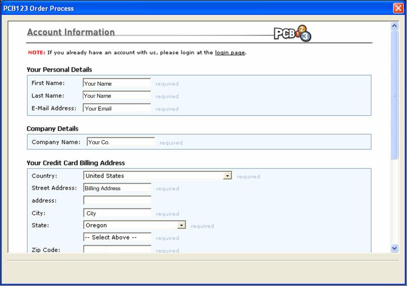
24 Account Screen


25 Shipping Address Information Payment Information


26 Confirm Order Checkout Confirmation

27 File Transfer Screen Shipping Methods As you fill out your information you will be asked for your choice of ship method. Once your order is completed your boards will be shipped. UPS orders will have the tracking number sent to the supplied address the evening the boards ship. You will have the convenience of checking the status of your order online. During the build process your order will show as "Processing". Once the order is completed and shipped, the status will change to "Shipped".
Exercise 1. Section 2. Working in Capture
 Exercise 1 Section 1. Introduction In this exercise, a simple circuit will be drawn in OrCAD Capture and a netlist file will be generated. Then the netlist file will be read into OrCAD Layout. In Layout,
- create new schematic to the new project, PCB design begins with a schematic diagram, which present how components are connected
 Eagle 8.x tutorial - create a new project, Eagle designs are organized as projects - create new schematic to the new project, PCB design begins with a schematic diagram, which present how components are
Schematic Editing Essentials
 Summary Application Note AP0109 (v2.0) March 24, 2005 This application note looks at the placement and editing of schematic objects in Altium Designer. This application note provides a general overview
CADSOFT EAGLE TUTORIAL
 CADSOFT EAGLE TUTORIAL IEEE OPS 2013-2014 By Shubham Gandhi, Kamal Kajouke 1 Table of Contents 1. Introduction 1.1 Getting Started 1.2 Eagle Schematic Editor 1.3 The Toolbar and Command Bar 1.4 Importing
TUTORIAL SESSION Technical Group Hoda Najafi & Sunita Bhide
 TUTORIAL SESSION 2014 Technical Group Hoda Najafi & Sunita Bhide SETUP PROCEDURE Start the Altium Designer Software. (Figure 1) Ensure that the Files and Projects tabs are located somewhere on the screen.
Orcad Layout Plus Tutorial
 Orcad Layout Plus Tutorial Layout Plus is a circuit board layout tool that accepts a layout-compatible circuit netlist (ex. from Capture CIS) and generates an output layout files that suitable for PCB
Introduction to PCB Design with EAGLE. Jianan Li
 Introduction to PCB Design with EAGLE Jianan Li Install EAGLE Download EAGLE: http://www.cadsoftusa.com/download-eagle/ Choose Run as Freeware during installation Create a New Project Launch EAGLE and
Instructions for designing the HelloWorld circuit board using Autodesk Eagle 8.6.0
 Instructions for designing the HelloWorld circuit board using Autodesk Eagle 8.6.0 FABLAB BRIGHTON 2018 These instructions take you through step-by-step the process of creating the full circuit board design
VLSI Lab Tutorial 3. Virtuoso Layout Editing Introduction
 VLSI Lab Tutorial 3 Virtuoso Layout Editing Introduction 1.0 Introduction The purpose of this lab tutorial is to guide you through the design process in creating a custom IC layout for your CMOS inverter
Osmond Tutorial. First Page / J C Chavez / / Osmond Tutorial
 Osmond Tutorial Draft Version corresponding to Osmond PCB Design Version 1.0b2 November 30, 2002 J C Chavez http://www.swcp.com/~jchavez/osmond.html jchavez@swcp.com First Page / J C Chavez / jchavez@swcp.com
Lesson 11: Interactive Routing and Glossing
 11 Lesson 11: Interactive Routing and Glossing Learning Objectives In this lesson you will: Define and display etch grids used for routing Create via fanouts Add and delete connect lines (clines) and vias
Creating a PCB Design with OrCAD PCB Editor
 Creating a PCB Design with OrCAD PCB Editor This guide is focused on learning how to create a PCB (Printed Circuit board) design. The guide will make use of the PCB Flow menu that is part of this workshop
GraphWorX64 Productivity Tips
 Description: Overview of the most important productivity tools in GraphWorX64 General Requirement: Basic knowledge of GraphWorX64. Introduction GraphWorX64 has a very powerful development environment in
Tutorial 3: Using the Waveform Viewer Introduces the basics of using the waveform viewer. Read Tutorial SIMPLIS Tutorials SIMPLIS provide a range of t
 Tutorials Introductory Tutorials These tutorials are designed to give new users a basic understanding of how to use SIMetrix and SIMetrix/SIMPLIS. Tutorial 1: Getting Started Guides you through getting
Autodesk Inventor Design Exercise 2: F1 Team Challenge Car Developed by Tim Varner Synergis Technologies
 Autodesk Inventor Design Exercise 2: F1 Team Challenge Car Developed by Tim Varner Synergis Technologies Tim Varner - 2004 The Inventor User Interface Command Panel Lists the commands that are currently
Lesson 5: Board Design Files
 5 Lesson 5: Board Design Files Learning Objectives In this lesson you will: Use the Mechanical Symbol Editor to create a mechanical board symbol Use the PCB Design Editor to create a master board design
EAGLE 6.x.x. University of Applied Sciences Ravensburg-Weingarten. EAGLE Tutorial. Author: Christian Schmid
 University of Applied Sciences Ravensburg-Weingarten EAGLE Tutorial EAGLE 6.x.x Author: Christian Schmid christian.schmid@hsweingarten.de Author: Martin Meier martin.meier@hs-weingarten.de September 30,
Lesson 9: Advanced Placement Techniques
 9 Lesson 9: Advanced Placement Techniques Learning Objectives In this lesson you will: Turn ratsnests on and off to selectively place components Use interactive swapping for pins and gates Apply advanced
VLSI Lab Tutorial 1. Cadence Virtuoso Schematic Composer Introduction
 VLSI Lab Tutorial 1 Cadence Virtuoso Schematic Composer Introduction 1.0 Introduction The purpose of the first lab tutorial is to help you become familiar with the schematic editor, Virtuoso Schematic
Tutorial : First board in CircuitMaker.
 Tutorial : First board in CircuitMaker. Objectives 1. Create a new project in CircuitMaker. 2. Design electronic circuit in CircuitMaker schematic editor. 3. Design a pcb board for your circuit in CircuitMaker
Design rule illustrations for the AMI C5N process can be found at:
 Cadence Tutorial B: Layout, DRC, Extraction, and LVS Created for the MSU VLSI program by Professor A. Mason and the AMSaC lab group. Revised by C Young & Waqar A Qureshi -FS08 Document Contents Introduction
Lesson 11: Routing and Glossing
 11 Lesson 11: Routing and Glossing Learning Objectives In this lesson you will: Define and display etch grids used for routing Create via fanouts Add and delete connect lines (clines) and vias Use Slide
StickFont Editor v1.01 User Manual. Copyright 2012 NCPlot Software LLC
 StickFont Editor v1.01 User Manual Copyright 2012 NCPlot Software LLC StickFont Editor Manual Table of Contents Welcome... 1 Registering StickFont Editor... 3 Getting Started... 5 Getting Started...
Procedure for PCBoard Layout
 Procedure for PCBoard Layout Introduction The following 6 pages of instructions will take you step by step through the creation of your PCB using Orcad Layout. If you are planning to manually lay out your
Introduction to NI Multisim & Ultiboard
 George Washington University School of Engineering and Applied Science Electrical and Computer Engineering Department Introduction to NI Multisim & Ultiboard Dr. Amir Aslani 8/20/2017 2 Outline Design
Experiment 1 Electrical Circuits Simulation using Multisim Electronics Workbench: An Introduction
 Experiment 1 Electrical Circuits Simulation using Multisim Electronics Workbench: An Introduction Simulation is a mathematical way of emulating the behavior of a circuit. With simulation, you can determine
Designing a PCB using EagleCAD
 Designing a PCB using EagleCAD Atlanta Hobby Robot Club Yes, you can design your own custom PCB and this tutorial will show you how. It is easier than ever to design your own PCB and having it manufactured
Getting started in the PCB Editor
 Getting started in the PCB Editor by Lori Zukerman of the EE/CAD group 01/07/04 Page 1 of 21 1. Initial Setup... 3 1.1 Copying Drawing Formats... 3 2. Starting your PCB... 3 2.1 Open a setup drawing...
Construction of Industrial Electronic Equipments
 VSB-Technical university of Ostrava Faculty of Electrical Engineering and Computer Science Department of electronics Construction of Industrial Electronic Equipments Syllabus Part 2 PCB Design and Fabrication
PADS-PowerPCB 4 Tutorial (with Blazeroute)
") PADS-PowerPCB 4 Tutorial (with Blazeroute) PADS-PowerPCB is the ultimate design environment for complex, high-speed printed circuit boards. PROCEDURE FOR SIMULATION IN SCHEMATICS 1. Importing Design Data
PADS-PowerPCB 4 Tutorial (with Blazeroute) PADS-PowerPCB is the ultimate design environment for complex, high-speed printed circuit boards. PROCEDURE FOR SIMULATION IN SCHEMATICS 1. Importing Design Data
Controlling the Drawing Display
 Controlling the Drawing Display In This Chapter 8 AutoCAD provides many ways to display views of your drawing. As you edit your drawing, you can control the drawing display and move quickly to different
How to Get Started. Figure 3
 Tutorial PSpice How to Get Started To start a simulation, begin by going to the Start button on the Windows toolbar, then select Engineering Tools, then OrCAD Demo. From now on the document menu selection
4 TRANSFORMING OBJECTS
 4 TRANSFORMING OBJECTS Lesson overview In this lesson, you ll learn how to do the following: Add, edit, rename, and reorder artboards in an existing document. Navigate artboards. Select individual objects,
EAGLE 3.5 Schematic - Layout - Autorouter Tutorial Copyright 1999 CadSoft Computer, Inc.
 EAGLE 3.5 Schematic - Layout - Autorouter Tutorial Copyright 1999 CadSoft Computer, Inc. www.cadsoftusa.com Windows is a registered trademark of Microsoft Corporation 1 What to expect from this Manual
ELEC451 Integrated Circuit Engineering Using Cadence's Virtuoso Layout Editing Tool
 ELEC451 Integrated Circuit Engineering Using Cadence's Virtuoso Layout Editing Tool Contents Contents 1. General 2. Creating and Working On a Layout o 2.1 Undoing/Re-doing an Action o 2.2 Display Options
MET 107 Drawing Tool (Shapes) Notes Day 3
 Notes Day 3") MET 107 Drawing Tool (Shapes) Notes Day 3 Shapes: (Insert Tab Shapes) Example: Select on the rounded rectangle Then use the mouse to position the upper left corner and produce the size by dragging out
MET 107 Drawing Tool (Shapes) Notes Day 3 Shapes: (Insert Tab Shapes) Example: Select on the rounded rectangle Then use the mouse to position the upper left corner and produce the size by dragging out
Editing Multiple Objects. Contents
 Editing Multiple Objects Contents Selecting Multiple Objects Inspecting the Objects Editing the Objects Editing Group Objects Step 1. Selecting the Capacitors Step 2. Changing the Comment String Step 3.
Using OrCAD Layout Plus A Simple Guide
 Using OrCAD Layout Plus A Simple Guide Written by Jose Cabral September 2006 Revised by Nithin Raghunathan 1 SKETCH THE CIRCUIT YOU WISH TO LAYOUT SKETCH THE LAYOUT COM J1 OUTPUT +12 COM -12 COM INPUT
Welcome to MicroStation
 Welcome to MicroStation Module Overview This module will help a new user become familiar with the tools and features found in the MicroStation design environment. Module Prerequisites Fundamental knowledge
Department of Electrical and Electronics Engineering SSN College of Engineering
 1 Department of Electrical and Electronics Engineering SSN College of Engineering 2 TABLE OF CONTENTS EAGLE CADSOFT Professional 2 Getting Started 3 Toolbar quick reference 5 Creating the Schematic 6 Creating
EE 210 Lab Assignment #2: Intro to PSPICE
 EE 210 Lab Assignment #2: Intro to PSPICE ITEMS REQUIRED None Non-formal Report due at the ASSIGNMENT beginning of the next lab no conclusion required Answers and results from all of the numbered, bolded
Prototype PCBs design session
 Prototype PCBs design session By: Dr. Ahmed ElShafee ١ Dr. Ahmed ElShafee, ACU : Spring 2018, EEP04 Practical Applications in Electrical Before start You will be making a schematic (astable.sch) file which
UNIVERSITY OF CALIFORNIA, DAVIS Department of Electrical and Computer Engineering. EEC180A DIGITAL SYSTEMS I Winter 2015
 UNIVERSITY OF CALIFORNIA, DAVIS Department of Electrical and Computer Engineering EEC180A DIGITAL SYSTEMS I Winter 2015 LAB 1: Introduction to Quartus II Schematic Capture and ModelSim Simulation This
3ds Max Cottage Step 1. Always start out by setting up units: We re going with this setup as we will round everything off to one inch.
 3ds Max Cottage Step 1 Always start out by setting up units: We re going with this setup as we will round everything off to one inch. File/Import the CAD drawing Be sure Files of Type is set to all formats
Netscape Composer: Working with Tables
 Why tables? Netscape Composer: Working with Tables Tables on the Web can be divided into two categories: data display and page layout. Although the method for making both kinds of tables is the same, it
Lesson 1: Getting Started with OrCAD Capture
 1 Lesson 1: Getting Started with OrCAD Capture Lesson Objectives Discuss design flow using OrCAD Capture Learn how to start OrCAD Capture The OrCAD Capture Start Page Open an existing Project Explore the
Getting Started with PCB Design
 Getting Started with PCB Design Summary Tutorial TU0117 (v1.2) April 13, 2005 This introductory tutorial is designed to give you an overview of how to create a schematic, update the design information
2008 년안산일대디지털정보통신학과 CAD 강의용자료 PADS 2007
 2008 년안산일대디지털정보통신학과 CAD 강의용자료 PADS 2007 1 Learning the PADS User Interface What you will learn: Modeless Commands Panning & Zooming Object Selection Methods Note: This tutorial will use PADS Layout to
Lesson 17: Building a Hierarchical Design
 Lesson 17: Building a Hierarchical Design Lesson Objectives After you complete this lesson you will be able to: Explore the structure of a hierarchical design Editing the Training Root Schematic Making
Verifying the Multiplexer Layout
 4 This chapter introduces you to interactive verification. You will perform two different tests in the Virtuoso layout editor while using Assura interactive verification products. One test uses the Design
Table of Contents. Part I Introduction. Part II Creating a simple Schematic and PCB. Part III Creating Libraries.
 TUTORIAL 2 DipTrace Tutorial Table of Contents Part I Introduction 4 Part II Creating a simple Schematic and PCB 4 1 Establishing a... schematic size and placing titles 5 2 Configuring libraries... 8 3
Beginning Tutorial the Lego
 Beginning Tutorial the Lego In this tutorial, you will construct a simple hollowed-out block with a hole in it (looks like a Lego). You will learn the basics of creating and modifying sketches and features.
Introduction to Electronics Workbench
 Introduction to Electronics Workbench Electronics Workbench (EWB) is a design tool that provides you with all the components and instruments to create board-level designs on your PC. The user interface
Constructing and Producing a Printed Circuit Board
 Constructing and Producing a Printed Circuit Board Craig Zofchak Design Team 8 11/07/2008 Abstract When a circuit in its development phase is finished and working correctly, it is then necessary to take
Learning to use the drawing tools
 Create a blank slide This module was developed for Office 2000 and 2001, but although there are cosmetic changes in the appearance of some of the tools, the basic functionality is the same in Powerpoint
SILVACO. An Intuitive Front-End to Effective and Efficient Schematic Capture Design INSIDE. Introduction. Concepts of Scholar Schematic Capture
 TCAD Driven CAD A Journal for CAD/CAE Engineers Introduction In our previous publication ("Scholar: An Enhanced Multi-Platform Schematic Capture", Simulation Standard, Vol.10, Number 9, September 1999)
Piping Design. Site Map Preface Getting Started Basic Tasks Advanced Tasks Customizing Workbench Description Index
 Piping Design Site Map Preface Getting Started Basic Tasks Advanced Tasks Customizing Workbench Description Index Dassault Systèmes 1994-2001. All rights reserved. Site Map Piping Design member member
Polygon Pour. Summary. Availability. Modified by on 19-Nov Parent page: Objects
 Polygon Pour Old Content - visit altium.com/documentation Modified by on 19-Nov-2013 Parent page: Objects A Polygon Pour (brighter red) being used to create a large GND area on a board. Summary A polygon
Electronics Design - Eagle
 Back to tutorial index Electronics Design - Eagle This week's assignment is to: add a button and LED to the echo hello-world board, check the design rules, and make it. Review Neil's class page: http://academy.cba.mit.edu/classes/electronics_design/index.html
Tutorial 01 Quick Start Tutorial
 Tutorial 01 Quick Start Tutorial Homogeneous single material slope No water pressure (dry) Circular slip surface search (Grid Search) Intro to multi scenario modeling Introduction Model This quick start
What is Publisher, anyway?
 What is Publisher, anyway? Microsoft Publisher designed for users who need to create and personalize publications such as marketing materials, business stationery, signage, newsletters and other items
OpenForms360 Validation User Guide Notable Solutions Inc.
 OpenForms360 Validation User Guide 2011 Notable Solutions Inc. 1 T A B L E O F C O N T EN T S Introduction...5 What is OpenForms360 Validation?... 5 Using OpenForms360 Validation... 5 Features at a glance...
DipTrace Tutorial Table of Contents Part I Introduction Part II Creating a simple Schematic and PCB
 TUTORIAL 2 DipTrace Tutorial Table of Contents Part I Introduction 4 Part II Creating a simple Schematic and PCB 4 1 Establishing... schematic size and placing titles 5 2 Configuring... libraries 9 3 Designing...
Placement & Routing. Lab 8. Placing Parts
 Placement & Routing Lab 8 Placing Parts 121 Placement and Routing Lab 8: Placing Parts This lesson will show you how to place parts in PADS Layout. Placement can be driven from the schematic or directly
Introduction to SolidWorks Basics Materials Tech. Wood
 Introduction to SolidWorks Basics Materials Tech. Wood Table of Contents Table of Contents... 1 Book End... 2 Introduction... 2 Learning Intentions... 2 Modelling the Base... 3 Modelling the Front... 10
CHAPTER 1 COPYRIGHTED MATERIAL. Getting to Know AutoCAD. Opening a new drawing. Getting familiar with the AutoCAD and AutoCAD LT Graphics windows
 CHAPTER 1 Getting to Know AutoCAD Opening a new drawing Getting familiar with the AutoCAD and AutoCAD LT Graphics windows Modifying the display Displaying and arranging toolbars COPYRIGHTED MATERIAL 2
University of Kansas EECS Circuit Board Fabrication Tutorial for 212 Lab
 University of Kansas EECS Circuit Board Fabrication Tutorial for 212 Lab Preparing For Export... 1 Assigning Footprints... 1 Recommended Footprints... 2 No Connects... 3 Design Rules Check... 3 Create
Basic Modeling 1 Tekla Structures 12.0 Basic Training September 19, 2006
 Tekla Structures 12.0 Basic Training September 19, 2006 Copyright 2006 Tekla Corporation Contents Contents 3 1 5 1.1 Start Tekla Structures 6 1.2 Create a New Model BasicModel1 7 1.3 Create Grids 10 1.4
EDITING SHAPES. Lesson overview
 3 CREATING AND EDITING SHAPES Lesson overview In this lesson, you ll learn how to do the following: Create a document with multiple artboards. Use tools and commands to create basic shapes. Work with drawing
Autodesk Inventor - Basics Tutorial Exercise 1
 Autodesk Inventor - Basics Tutorial Exercise 1 Launch Inventor Professional 2015 1. Start a New part. Depending on how Inventor was installed, using this icon may get you an Inch or Metric file. To be
Apex Sketch v7. Define First
 Apex Sketch v7 Legacy Draw First Drawing Method Define First Apex Sketch Version 7 Define First Apex Sketch Version 7 uses the same keystrokes as you would use traditionally in any other Apex program.
HW #2 - Eagle Tutorial
 HW #2 - Eagle Tutorial The goal of this homework is to teach the user the basic steps of producing a switching power supply schematic and a printed circuit board using the Eagle Application. While tutorial
3D Body. Summary. Modified by Admin on Sep 13, Parent page: Objects
 3D Body Old Content - visit altium.com/documentation Modified by Admin on Sep 13, 2017 Parent page: Objects A sphere, a cylinder and 4 extruded rectangles have been used to create the 3D body for an LED.
Technique or Feature Where Introduced
 Part 6: Keypad 4 Mirrored features Patterned features First extrusion Rounded corners In the earpiece part, you defined a radial pattern, one that created new instances of a feature at intervals around
SIMPLE TEXT LAYOUT FOR COREL DRAW. When you start Corel Draw, you will see the following welcome screen.
 SIMPLE TEXT LAYOUT FOR COREL DRAW When you start Corel Draw, you will see the following welcome screen. A. Start a new job by left clicking New Graphic. B. Place your mouse cursor over the page width box.
Quick Crash Scene Tutorial
 Quick Crash Scene Tutorial With Crash Zone or Crime Zone, even new users can create a quick crash scene diagram in less than 10 minutes! In this tutorial we ll show how to use Crash Zone s unique features
Using Adobe Photoshop
 Using Adobe Photoshop 2 In this section we ll look at some essential things you need to know in order to use Photoshop effectively. First of all, we ll take a look at customising Photoshop s settings and
Working with PDF s. To open a recent file on the Start screen, double click on the file name.
 Working with PDF s Acrobat DC Start Screen (Home Tab) When Acrobat opens, the Acrobat Start screen (Home Tab) populates displaying a list of recently opened files. The search feature on the top of the
Lesson 8: Component Placement
 8 Lesson 8: Component Placement Learning Objectives In this lesson you will: Using floorplanning to organize the placement of components with the same ROOM property Assign reference designators to preplaced
Design capture, simulation and layout - an introduction Tutorial
 Design capture, simulation and layout - an introduction Tutorial A step-by-step introduction to Altium s complete board-level design system 1 Software, documentation and related materials: Copyright 2002
Status Bar: Right click on the Status Bar to add or remove features.
 Excel 2013 Quick Start Guide The Excel Window File Tab: Click to access actions like Print, Save As, etc. Also to set Excel options. Ribbon: Logically organizes actions onto Tabs, Groups, and Buttons to
PCB Design utilizing Cadence Software. Application Note
 PCB Design utilizing Cadence Software Application Note Kyle Schultz 11-9-11 ECE 480 Design Team 5 Keywords: Schematic, PCB, Fabrication, Cadence, Design Entry CIS, Allegro Table of Contents Abstract 1
EE115C Digital Electronic Circuits. Tutorial 4: Schematic-driven Layout (Virtuoso XL)
") EE115C Digital Electronic Circuits Tutorial 4: Schematic-driven Layout (Virtuoso XL) This tutorial will demonstrate schematic-driven layout on the example of a 2-input NAND gate. Simple Layout (that won
EE115C Digital Electronic Circuits Tutorial 4: Schematic-driven Layout (Virtuoso XL) This tutorial will demonstrate schematic-driven layout on the example of a 2-input NAND gate. Simple Layout (that won
1 General Principles. General Principles. In this chapter 1-1
 1 General Principles In this chapter 1 General Principles 1.1 User Interface 1.2 Title bar 1.3 Menu bar 1.4 Standard Toolbar 1.5 The drawing area 1.6 Component tabs 1.7 Status Bar 1.8 Manipulating Components
Adobe Acrobat Reader 4.05
 Adobe Acrobat Reader 4.05 1. Installing Adobe Acrobat Reader 4.05 If you already have Adobe Acrobat Reader installed on your computer, please ensure that it is version 4.05 and that it is Adobe Acrobat
A Quick EAGLE PCB Tutorial
 A Quick EAGLE PCB Tutorial Tim Steffes Mark Brehob 9/17/11 Introduction So, you ve finished your circuit prototype and you re ready to make it permanent? Tired of those messy wires and loose components,
Fusion. CBR Fusion MLS Level 1 Core Functions. Class Handout
 Fusion 1 CBR Fusion MLS Level 1 Core Functions Class Handout GETTING STARTED IN FUSION Logging On and Off To log on to Fusion MLS: 1. Type your user name in the User ID box. 2. Type your password in the
ECSE-323 Digital System Design. Lab #1 Using the Altera Quartus II Software Fall 2008
 1 ECSE-323 Digital System Design Lab #1 Using the Altera Quartus II Software Fall 2008 2 Introduction. In this lab you will learn the basics of the Altera Quartus II FPGA design software through following
PLAY VIDEO. Fences can be any shape from a simple rectangle to a multisided polygon, even a circle.
 Chapter Eight Groups PLAY VIDEO INTRODUCTION There will be times when you need to perform the same operation on several elements. Although this can be done by repeating the operation for each individual
ILLUSTRATOR. Introduction to Adobe Illustrator. You will;
 ILLUSTRATOR You will; 1. Learn Basic Navigation. 2. Learn about Paths. 3. Learn about the Line Tools. 4. Learn about the Shape Tools. 5. Learn about Strokes and Fills. 6. Learn about Transformations. 7.
Virtuoso Layout Editor
 This tutorial will cover the basic steps involved in using the Cadence layout editor called Virtuoso, extracting layout, and running simulation on the layout. The inverter layout is used as an example
Press the Plus + key to zoom in. Press the Minus - key to zoom out. Scroll the mouse wheel away from you to zoom in; towards you to zoom out.
 Navigate Around the Map Interactive maps provide many choices for displaying information, searching for more details, and moving around the map. Most navigation uses the mouse, but at times you may also
Cadence Tutorial A: Schematic Entry and Functional Simulation Created for the MSU VLSI program by Andrew Mason and the AMSaC lab group.
 Cadence Tutorial A: Schematic Entry and Functional Simulation Created for the MSU VLSI program by Andrew Mason and the AMSaC lab group. Revision Notes: Aug. 2003 update and edit A. Mason add intro/revision/contents
Lesson 18: Creating a Hierarchical Block
 Lesson 18: Creating a Hierarchical Block Lesson Objectives After you complete this lesson you will be able to: Create hierarchical blocks Copying Schematics between Projects You can copy and paste between
Revision Notes: July2004 Generate tutorial for single transistor analysis. Based on existing schematic entry tutorial developed for ECE410
 Cadence Analog Tutorial 1: Schematic Entry and Transistor Characterization Created for the MSU VLSI program by Professor A. Mason and the AMSaC lab group. Revision Notes: July2004 Generate tutorial for
Chapter 4 Determining Cell Size
 Chapter 4 Determining Cell Size Chapter 4 Determining Cell Size The third tutorial is designed to give you a demonstration in using the Cell Size Calculator to obtain the optimal cell size for your circuit
KiCad Example Schematic ( ) Wien Bridge Oscillator
 Wien Bridge Oscillator") KiCad Example Schematic (2010-05-05) Wien Bridge Oscillator University of Hartford College of Engineering, Technology, and Architecture The following tutorial in that it walks you through steps to use
KiCad Example Schematic (2010-05-05) Wien Bridge Oscillator University of Hartford College of Engineering, Technology, and Architecture The following tutorial in that it walks you through steps to use
Word 2013 Quick Start Guide
 Getting Started File Tab: Click to access actions like Print, Save As, and Word Options. Ribbon: Logically organize actions onto Tabs, Groups, and Buttons to facilitate finding commands. Active Document
Getting Started. In This Chapter
 Getting Started In This Chapter 2 This chapter introduces concepts and procedures that help you get started with AutoCAD. You learn how to open, close, and manage your drawings. You also learn about the
Lesson 5: Creating Heterogeneous Parts
 Lesson 5: Creating Heterogeneous Parts Lesson Objectives After you complete this lesson you will be able to: Create a Heterogeneous part Annotate a Heterogeneous part (Optional) Heterogeneous Parts A heterogeneous