MICROPROCESSOR QUESTION BANK. Unit 1
|
|
|
- Louise Warren
- 5 years ago
- Views:
Transcription
1 QUESTION BANK Unit 1 1. Explain the term Microprocessor. ( CO1-K2) A microprocessor is a multipurpose, programmable logic device that receives binary instructions from a storage device called memory accepts binary data as input and processes data according to those instructions and provides result as output. 2. Classify the BUS. ( CO1-K2) Bus: Group of wires carrying information. Address bus: An address bus is a computer bus that is used to specify a physical address. Data bus: It provides transportation for data. Control bus: It carries signals that report the status of various devices. 3. Compare CMP and SUB instruction of 8086.( CO1-K2) After execution of an instruction, CMP It affects the flag SUB- It doesn t affect the flag 4. What is an Assembler Directive? (CO1-K1) Assembler directives help the assembler to correctly understand the assembly language programs to prepare the codes. There are some instructions in the assembly language program which are not part of processor instruction set. These instructions are instructions to the assembler, linker and loader. These are called as Pseudo operations or as Assembler directives. 5. Outline about operand and opcode. ( CO1-K2) Operand It specifies the type of operation to be performed. Op code data needs for completing the task 6. Compare Maskable and Nonmaskable interrupts.(co1-k2) The interrupts whose request can be either accepted or rejected by the processor are called maskable interrupts. The interrupts whose request has to be definitely accepted (or cannot be rejected) by the processor are called non-maskable interrupts. 7. What is Procedure?(CO1-K1) The procedure is a group of instructions stored as a separate program in the memory and it is called from the main program whenever required. The type of procedure depends on where 1
2 the procedure is stored in the memory. If it is in the same code segment where the main program is stored then it is called near procedure otherwise it is referred to as far procedure. 8. What is Recursive procedure? (CO1-K1) Recursive procedure is a procedure which calls itself. If the procedure is called 4 times, then it is decremented by one after each procedure CALL and the procedure is called again and again until it reaches zero. 9. Tell the different ways of interrupting processor. (CO1-K1) The processor can be interrupted in the following ways: i) by an external signal generated by a peripheral, ii) by an internal signal generated b y a special instruction in the program, iii) by an internal signal generated due to an exceptional condition which occurs while executing an instruction. (For example, in 8086 processor, divide by zero is an exceptional condition which initiates type 0 interrupt and such an interrupt is also called execution). 2
3 10. Draw the diagram for pipeline operation.(co1-k1) UNIT 2 1. Explain the term Multiprocessor. (CO2-K2) Multiprocessor Systems refer to the use of multiple processors that execute instructions Simultaneously and communicate. 2. Classify the bus arbitration mechanism. (CO2- K2) Bus Arbitration: The mechanism which decided the selection of current master to access bus is known as Bus arbitration. Three mechanisms are normally used: 1. Daisy chaining. 2. Polling. 3. Independent requesting 3. Show the interaction between 8086 and 8087 in diagrammatic format.( CO2-K2) 3
4 4. Outline about single step Interrupt. (CO2-K2) As in 8086, this is an internal interrupt that comes into action, if trap flag (TF) of is set. The CPU stops the execution after each instruction cycle. So, that the register contents (including flag register), the program status word and memory, etc. may be examined at the end of each instruction execution. This interrupt is useful for troubleshooting the software. An interrupt vector type 01 is reserved for this interrupt. 5. Summarize the functions of the following signals in PEREG, PEACK. (CO2-K2) PEREG and PEACK (Processor Extension Request and Acknowledgement) Processor extension refers to coprocessor. This pair of pins extends the memory management and protection capabilities of to the processor extension The PEREQ input requests the to perform a data operand transfer for a processor extension. The PEACK active-low output indicates to the processor extension that the requested operand is being transferred. 6. Summarize the functions of the following signals in HOLD and HLDA. (CO2-K2) HOLD and HLDA: This pair of pins is used by external bus masters to request for the control of the system bus (HOLD) and to check whether the main processor has granted the control (HLDA) or not, in the same way as it was in Outline about single step Interrupt. (CO2-K2) As in 8086, this is an internal interrupt that comes into action, if trap flag (TF) of is set. 4
5 The CPU stops the execution after each instruction cycle. So, that the register contents (including flag register), the program status word and memory, etc. may be examined at the end of each instruction execution. This interrupt is useful for troubleshooting the software. An interrupt vector type 01 is reserved for this interrupt. 8. Short notes on Transcendental Instructions of (CO2-K2) FPTAN - Compute the values for a ration of Y/X for an angle in ST. The angle must be expressed in radians. F2XM1 Compute the function Y=2 x 1 for an X value in ST. Result will be stored in ST by replacing X value. 9. What is the importance of IOPL signal in 80286? (CO2-K2) IOPL Input Output Privilege Level flags (bit D12 and D13) IOPL is used in protected mode operation to select the privilege level for I/O devices. 10. What is the necessity of Memory Management unit?( CO2-K2) The part of main memory in which the operating system and other system programs are stored is not accessible to the users. In view of this, an appropriate management of the memory system is required to ensure the smooth execution of the running process and also to ensure their protection. The memory management which is an important task of the operating system is supported by a hardware unit called memory management unit. 1. What is the purpose of 8255? (CO3-K1) Unit 3 The 8255 is a widely used, programmable parallel I/O device. It can be programmed to transfer data under various conditions. It is flexible, versatile and economical (when multiple I/O ports are required). It is an important general purpose I/O device that can be used with almost any microprocessor. 2. What is the purpose of 8251? (CO3-K1) 8251 is a Universal Synchronous and Asynchronous Receiver and Transmitter compatible with Intel s processors. This chip converts the parallel data into a serial stream of bits suitable for serial transmission. It is also able to receive a serial stream of bits and convert it into parallel data bytes to be read by a microprocessor. 5
6 3. Compare Linear and Absolute decoding. (CO3-K2) In the absolute decoding technique the memory chip is selected only for the specified logic level on the address lines: no other logic levels can select the chip. This address technique is normally used in large memory systems. In small system hardware for the decoding logic can be eliminated by using only required number of addressing lines (not all). Other lines are simply ignored. This technique reduces the cost of decoding circuit, but it has drawback of multiple addresses. 4. Summarize input and output port. (CO3-K2) Input port: It is used to get the data from the input device such as keyboard and send it to the microprocessor. The simplest form of the input port is a buffer. 5. Summarize about Left entry and right entry mode. (CO3-K2) 1. Left Entry Mode In the Left entry mode, the data is entered from the left side of the display unit. Address 0 of the display RAM contains the leftmost display character and address 15 of the RAM contains the rightmost display character. 2. Right Entry Mode In the right entry mode, the first entry to be displayed is entered on the rightmost display. The next entry is also placed in the right most display but after the previous display is shifted left by one display position. 6. Outline about Mode 0 of (CO3-K2) Mode 1: Input or Output with handshake In mode 1, handshake signals are exchanged between the microprocessor and peripherals prior to data transfer. The ports (A and B) function as 8-bit I/O ports. They can be configured either as input or output ports. 6
7 Each port (Port A and Port B) uses 3 lines from port C as handshake signals. The remaining two lines of port C can be used for simple I/O functions. Input and output data are latched and Interrupt logic is supported. 7. What is cycle stealing? (CO3-K1) During any given bus cycle, one of the system components connected to the system bus is given control of the bus. This component is said to be the master during that cycle and the component it is communicating with is said to be the slave. The CPU with its bus control logic is normally the master, but other specially designed components can gain control of the bus by sending a bus request to the CPU. After the current bus cycle is completed the CPU will return a bus grant signal and the component sending the request will become the master. Taking control of the bus for a bus cycle is called cycle stealing. 8. How DMA operations are performed? (CO3-K1) Following is the sequence of operations performed by a DMA. Initially, when any device has to send data between the device and the memory, the device has to send DMA request (DRQ) to DMA controller. The DMA controller sends Hold request (HRQ) to the CPU and waits for the CPU to assert the HLDA. Then the microprocessor tri-states all the data bus, address bus, and control bus. The CPU leaves the control over bus and acknowledges the HOLD request through HLDA signal. Now the CPU is in HOLD state and the DMA controller has to manage the operations over buses between the CPU, memory, and I/O devices. The chip support four DMA channels, i.e. four peripheral devices can independently request for DMA data transfer through these channels at a time. 9. Compare Burst transfer and Hidden DMA. (CO3-K2) Burst Transfer: To achieve block transfers, some DMAC's incorporate an automatic sequencing of the value presented on the address bus. A register is used as a byte count, being decremented for each byte transfer, and upon the byte count reaching zero, the DMAC will release the bus. When the DMAC operates in burst mode, the CPU is halted for the duration of the data transfer. Hidden DMA: 7

8 It is possible to perform hidden DMA, which is transparent to the normal operation of the CPU. In other words, the bus is grabbed by the DMAC when the processor is not using it. The DMAC monitors the execution of the processor, and when it recognises the processor executing an instruction which has sufficient empty clock cycles to perform a byte transfer; it waits till the processor is decoding the op code, then grabs the bus during this time. 10. How does the master slave concept work? (CO3-K1) Unit 4 1. Compare Microprocessor and Microcontroller. (K2-CO4) 8
 3. Summarize about CISC of 8051.")
9 2. List out the application of (K1-CO4) 3. Summarize about CISC of (K2-CO4) 9

10 Memory in those days was expensive. Bigger programs required more storage which included more money. There was a need to reduce the number of instructions per program. This was achieved by having multiple operations within single instruction. Multiple operations lead to many different kinds of instructions. Access to memory in turn makes the instruction length variable and fetch-decode execute time unpredictable making it more complex. Thus hardware was made to understand the complexity of instruction set. The computer having such instruction set was named as Complex Instruction Set Computer (CISC). Intel 8051 is an example for CISC architecture. 4. Compare Von Neumann and Harward architecture. (K2-CO4) 5. What is an instruction cycle of 8051? (CO4-K1) The time taken to complete any instruction is called as machine cycle or instruction cycle. In 8051 one instruction cycle consists of 6 states or 12 clock cycles, instruction cycle is also referred as Machine cycle. 10
11 6. What is Microcontroller? A single chip computer or a CPU with all the peripherals like AM,ROM, I/O, Timers, ADCs, etc on the same chip. 7. Show the internal RAM structure of What are the use oftimer/ Counter? (CO4-K1) Timers/Counters are used generally for Time reference Creating delay Wave form properties measurement Periodic interrupt generation Waveform generation 11
12 9. Define an Instruction cycle Instruction cycle is defined as the time required for completing the execution of an instruction. The 8051 instruction cycle consists of one to four machine cycles. 10. What is an addressing mode? Short notes on Bit inherent addressing mode of Various methods of accessing the data are called addressing modes. Bit Inherent addressing mode In this addressing, the address of the flag which contains the operand, is implied in the opcode of the instruction. Eg. CLR C ; Clears the carry flag to 0 Unit 5 1. Summarize about interfacing of keyboard to the ( CO5 K2) Keyboards are organized in a matrix of rows and columns. The CPU accesses both rows and columns through ports; therefore, with two 8-bit ports, an 8 x 8 matrix of keys can be connected to a microprocessor. When a key is pressed, a row and a column make a contact; otherwise, there is no connection between rows and columns. 2. Show the diagram of matrix keyboard connection to ports. (CO5-K2) 3. What are the steps have been taken while processing an interrupt? (CO5-K1) 1. It completes the execution of the current instruction. 2. PSW is pushed to stack. 3. PC content is pushed to stack. 4. Interrupt flag is reset. 12
13 5. PC is loaded with ISR address. 4. Show the structure of Interrupt Enable register of Show the structure of Interrupt Priority register of Summarize about modes of timer in (CO5-K2) Mode 0: This is a 13-bit mode that means the timer operation completes with 8192 pulses. Mode 1: This is a16-bit mode, which means the timer operation completes with maximum clock pulses that
14 Mode 2: This mode is an 8-bit auto reload mode, which means the timer operation completes with only 256 clock pulses. Mode 3: This mode is a split-timer mode, which means the loading values in T0 and automatically starts the T1. 7. Write the steps for programming timers in mode 1 (8051). (CO5-K1) Load the TMOD value register indicating which timer (0 or 1) is to be used and which timer mode is selected. Load registers TL and TH with initial count values. Start the timer by the instruction SETB TR0 for timer 0 and SETB TR1 for timer 1. Keep monitoring the timer flag (TF) with the JNB TFx, target instruction to see if it is raised. Get out of the loop when TF becomes high. Stop the timer with the instructions CLR TR0 or CLR TR1, for timer 0 and timer 1, respectively. Clear the TF flag for the next round with the instruction CLR TF0 or CLR TF1, for timer 0 and timer 1, respectively. Go back to step 2 to load TH and TL again. 8. Define A/D and D/A converters. (CO5-K1) D/A converters transform a digital signal to an equivalent analog signal, and A/D converters transform an analog signal to an equivalent digital signal. 9. Define serial to parallel conversion? (CO5-K1) In serial reception, the MPU receives a stream of eight bits and it is converted in to 8-bit parallel word. This is known as serial to parallel conversion. 10. Explain the 16-bit registers DPTR and SP of (CO5-K2) DPTR: DPTR stands for data pointer. DPTR consists of a high byte (DPH) and a low byte (DPL). Its function is to hold a 16-bit address. It may be manipulated as a 16-bitdata register or as two independent 8-bit registers. It serves as a base register in indirect jumps, lookup table instructions and external data transfer. Descriptive Questions (13 Marks) Unit 1 1. Explain about the internal architecture of (CO1-K2) ARCHITECTURE OF
 Arithmetic and logic unit (ALU): performs math and logical operations on command by the EU. 3) Internal storage (sometime called registers): is used for internal data storage.")
15 The 8086 microprocessor consists of four functional units. 1) Execution unit (EU): decodes and executes machine instructions. 2) Arithmetic and logic unit (ALU): performs math and logical operations on command by the EU. 3) Internal storage (sometime called registers): is used for internal data storage. 4) Bus interface unit (BIU): handles all communications with the I/O via the system bus and maintains instruction queue. BUS INTERFACE UNIT: BIU is a circuitry to response memory access and communicate with I/O devices.biu avoids idle time and hold an instruction queue such that instructions can be executed in a pipeline fashion. The bus interface unit is responsible for performing all external bus operations, as listed below: Functions of BIU: It sends address of the memory or I/O It fetches instruction from memory It reads data from port/memory 15
16 It writes data into port/memory Instruction Queue: To speed up program execution, the BIU fetches six instruction bytes ahead of time from the memory. These prefetched instruction bytes are held for the execution unit in a group of registers called Queue. By queue, it is possible to fetch next instruction when current instruction in an execution. During execution time of an instruction BIU fetches the next instruction or instructions from memory into the instruction queue instead of remaining idle. The BIU continues this process as long as the queue is not full. Due to this execution unit gets ready instruction in the queue and instruction fetch time is eliminated. This is illustrated in figure. The queue operates on principles first in first out (FIFO). So that the execution unit gets the instructions for execution in the order they are fetched. Incase JUMP and CALL instructions, 16
17 instructions already fetched in queue are of no use. Feature of fetching the next instruction while the current instruction is executing is called Pipelining. Execution unit: It contains the general, pointers and Index Registers, Arithmetic and Logic Unit, Control Unit and flags tells the BIU where to fetch instructions or data from, decodes instructions and executes instruction. The EU contains control circuitry which directs internal operations. A decoder in the EU translates instructions fetched from memory into a series of actions which the EU carries out. The EU is has a 16-bit ALU which can add, subtract, AND, OR, XOR, increment, decrement, complement or shift binary numbers. Flag Register: X X X X 0F DF IF TF SF ZF X AC X PF X CY Flags Register determines the current state of the processor. They are modified automatically by CPU after mathematical operations, this allows to determine the type of the result, and to determine conditions to transfer control to other parts of the program. The 8086 flag register as shown in the fig has 9 active flags and they are divided into two categories: 1. Conditional Flags 2. Control Flags 1. Conditional Flags 1. Carry Flag (CY): This flag is set if there is a carry out of the MSB during addition. The carry flag also serves as a borrow flag for subtraction. In case of subtraction it is set when borrow is needed. 2. Auxiliary Flag (AC): If an operation performed in ALU generates a carry/borrow from lower nibble (i.e. D0 - D3) to upper nibble (i.e. D4 - D7), the AC flag is set i.e. carry given by D3 bit to D4 is AC flag. This is not a general-purpose flag, it is used internally by the Processor to perform Binary to BCD conversion. 3. Parity Flag (PF): This flag is used to indicate the parity of result. If lower order 8- bits of the result contains even number of 1's, the Parity Flag is set and for odd number of 1's, the Parity flag is reset. 4. Zero Flag (ZF): It is set; if the result of arithmetic or logical operation is zero else it is reset. 5. Sign Flag (SF): In sign magnitude format the sign of number is indicated by MSB bit. If the result of operation is negative, sign flag is set. 17
18 Word Read: Each of 1 MB memory address of 8086 represents a byte wide location.16-bits words will be stored in two consecutive memory locations. If first byte of the data is stored at an even address, 8086 can read the entire word in one operation. For example if the 16 bit data is stored at even address 00520H is 9634H MOV BX, [00520H] 8086 reads the first byte and stores the data in BL and reads the 2nd byte and stores the data in BH BL= (00520H) i.e. BL=34H BH= (00521H) BH=96H If the first byte of the data is stored at an odd address, 8086 needs two operations to read the 16 bit data. For example if the 16 bit data is stored at odd address 00521H is 3897H MOV BX, [00521H] In first operation, 8086 reads the 16 bit data from the 00520H location and stores the data of 00521H location in register BL and discards the data of 00520H location. In 2nd operation, 8086 reads the 16 bit data from the 00522H location and stores the data of 00522H location in register BH and discards the data of 00523H location. BL= (00521H) i.e. BL=97H BH= (00522H) BH=38H Byte Read: MOV BH, [Addr] For Even Address: Example: MOV BH, [00520H] 8086 reads the first byte from location and stores the data in BH and reads the 2 nd byte from the 00521H location and ignores it. BH =[ 00520H] For Odd Address MOV BH, [Addr] Example: MOV BH, [00521H] 8086 reads the first byte from 00520H location and ignores it and reads the 2nd byte from the location and stores the data in BH. BH = [00521H] Register organization of 8086: All the registers of 8086 are 16-bit registers. The general purpose registers, can be used either 8-bit registers or 16-bit registers used for holding the data, variables and intermediate results temporarily or for other purpose like counter or for storing offset address for some 18

19 particular addressing modes etc. The special purpose registers are used as segment registers, pointers, index registers or as offset storage registers for particular addressing modes. AX Register: Accumulator register consists of two 8-bit registers AL and AH, which can be combined together and used as a 16- bit register AX. AL in this case contains the low-order byte of the word, and AH contains the high-order byte. Accumulator can be used for I/O operations, rotate and string manipulation. BX Register: This register is mainly used as a base register. It holds the starting base location of a memory region within a data segment. It is used as offset storage for forming physical address in case of certain addressing mode. CX Register: It is used as default counter - count register in case of string and loop instructions. DX Register: Data register can be used as a port number in I/O operations and implicit operand or destination in case of few instructions. In integer 32-bit multiply and divide instruction the DX register contains high-order word of the initial resulting number. Segment registers: Two types of memory organizations are commonly used. These are linear addressing and segmented addressing. In linear addressing the entire memory space is available to the processor in one linear array. In segmented addressing, the available memory space is divided into chunks called segments. Such a memory is called a segmented memory. In 8086 the available memory space is 1Mbytes. The memory is divided into number of logical segments. Each segment contains 64Kbyte of memory. There are four segment registers: Code segment, stack segment, Data segment and Extra segment. The 16-bit contents of the segment register gives the starting / base address of a particular segment as shown in figure. To address a specific memory location within a segment we need an offset address. The offset address is also 16-bit word and it is provided by one of the associated pointer or index register. 19
20 ***** 2. Explain the following addressing modes of (CO1-K2) 1. Addressing Modes for Accessing Immediate and Register Data 2. Addressing Modes for Accessing I/O Ports (I/O Modes) 3. Inter Segment and Intra Segment An instruction is divided into groups of bits or fields, with one field called the operation code (op code), indicating what the computer is to do, and the other fields, called the operands, indicating the information needed by the instruction in carrying out its task. An operand may contain a datum or part of the address of a datum. The addressing modes describe the types of operand and the way they are accessed for executing an instruction. Here, we will present the addressing modes of the instructions depending upon their types. According to the flow of instruction execution, the instructions may be categorized as (i) Sequential control flow instructions and (ii) Control transfer instructions. Sequential control flow instructions are the instructions, which after execution, transfer control to the next instruction appearing immediately after it (in the sequence) in the program. For example, the arithmetic, logical, data transfer and processor control instructions are sequential control flow instructions. The control transfer instructions, on the other hand, transfer 20
21 control to some predefined address somehow specified in the instruction after their execution. For example, INT, CALL, RET and JUMP instructions fall under this category. 1. Addressing Modes for Accessing Immediate and Register Data A. Immediate Addressing Mode: In this type of addressing, immediate data is a part of instruction, and appears in the form of successive byte or bytes. Example: MOV AX, 0005H MOV AL, 20 H In the above example, 0005H is the immediate data. The immediate data may be 8-bit or 16-bit in size. B. Register Addressing Mode: In register addressing mode, the data is stored in a register and it is referred using the particular register. This mode specifies the source operand, destination operand, or both to be contained in an 8080 register. All the registers, except IP, may be used in this mode. Example: MOV BX, AX. Copies the 16-bit contents of AX into BX MOV CL, BL Copies the 8-bit contents of BL into CL 2. Addressing Modes for Accessing I/O Ports (I/O Modes) A standard I/O device uses port addressing modes. Example: OUT 05H, AL Sends the contents of AL to 8-bit port 05 H IN AX, 80H - Copies 16-bit contents of port 80 H. IN AL, DX - IF [DX]= 7890H, then it copies 8-bit content of port 7890 H into AL. IN AX, DX - Copies the 8-bit contents of ports 7890 H and 7891 H into AL and AH, respectively. For the control transfer instructions, the addressing modes depend upon whether the destination location is within the same segment or a different one. It also depends upon the method of passing the destination address to the processor. Basically, there are two addressing modes for the control transfer instructions, viz. inter-segment and intra-segment addressing modes. 3. Inter Segment and Intra Segment If the location to which the control is to be transferred lies in a different segment other than the current one, the mode is called inter-segment mode. If the destination location lies in the same segment, the mode is called intra-segment. Intra-segment direct mode: In this mode, the address to which the control is to be transferred lies in the same segment in which the controls transfer instruction lies and appears directly in the instruction as an 21
22 immediate displacement value. In this addressing mode, the displacement is computed relative to the content of the instruction pointer IP. The effective address to which the control will be transferred is given by the sum of 8 or 16 bit displacement and current content of IP. In case of jump instruction, if the signed displacement (d) is of 8 bits (i.e. 128<d<+128), we term it as short jump and if it is of 16 bits (i.e <+32768), it is termed as long jump. Intra-segment Indirect Mode: In this mode, the displacement to which the control is to be transferred, is in the same segment in which the control transfer instruction lies, but it is passed to the instruction indirectly. Here, the branch address is found as the content of a register or a memory location. This addressing mode may be used in unconditional branch instructions. Inter-segment Direct Mode: In this mode, the address to which the control is to be transferred is in a different segment. This addressing mode provides a means of branching from one code segment to another code segment. Here, the CS and IP of the destination address are specified directly in the instruction. Inter-segment Indirect Mode: In this mode, the address to which the control is to be transferred lies in a different segment and it is passed to the instruction indirectly, i.e. contents of a memory block containing four bytes, i.e. IP (LSB), IP (MSB), CS (LSB) and CS (MSB) sequentially. The starting address of the memory block may be referred using any of the addressing modes, except immediate mode. ***** 3. Explain the following addressing modes of (CO1-K2) Addressing Modes for Accessing Data in Memory Addressing Modes for Accessing Data in Memory The Execution Unit (EU) has direct access to all registers and data for register and immediate operands. However, the EU cannot directly access the memory operands. It must use the BIU segment registers to access memory operands. When EU needs to access a memory location, it sends an offset value (off set value is also called the Effective address ) to the BIU. Effective address is displacement of the desired location from the segment base. BIU generates 20-bit physical address after shifting the contents of the desired segment registers four bits to the left and then adding the 16-bit EA to it. There are different ways to specify effective address (EA) in the instruction. a. Direct Addressing Mode: 22
23 In the direct addressing mode, a 16-bit memory address (offset) is directly specified in the instruction as a part of it. Example: MOV AL, [3000H] Here, data resides in a memory location in the data segment, whose effective address may be computed using 3000H as the offset address and content of DS as segment address. The effective address, here, is 10H*DS+3000H. Example: MOV [3000 H], CX b. Register Indirect addressing Mode: Sometimes, the address of the memory location, which contains data or operand, is determined in an indirect way, using the offset registers. This mode of addressing is known as register indirect mode. In this addressing mode, the offset address of data is in either BX or SI or DI registers. The default segment is either DS or ES. The data is supposed to be available at the address pointed to by the content of any of the above registers in the default data segment. Example: MOV BX, [CX] 23
24 The effective address of the data is given as 10H*DS+ [CX]. Example: MOV [DI], BX The instruction copies the 16-bit contents of BX into a memory location offset by the value of EA specified in DI from the current location contents in DS. If DS = 8205 H, [DI] = 0030 H and [BX]= 1020 H, then after MOV instruction content of BX ( 1020 H) is copied to memory locations H and H. C. Base plus Index Addressing Mode: The effective address of data is formed, in this addressing mode, by adding content of a base register (any one of BX or BP) to the content of an index register (any one of SI or DI). The default segment register may be ES or DS. Example: MOV AX, [BX] [SI] Here, BX is the base register and SI is the index register. The effective address is computed as 10H*DS+ [BX] + [SI]. Example: MOV CX, [BX+DI] 24
25 d. Register Relative Addressing Mode: In this addressing mode, the data is available at an effective address formed by adding an 8-bit or 16-bit displacement with the content of any one of the registers BX, BP, SI and DI in the default (either DS or ES) segment. The example given before explains this mode. Example: MOV CX, [BX+0003H] 25
26 e. Indexed: In this addressing mode, offset of the operand is stored in one of the index registers. DS and ES are the default segments for index registers SI and DI respectively. This mode is a special case of the above discussed register indirect addressing mode. Base Relative plus Index Addressing Mode: The effective address is formed by adding an 8-bit or 16-bit displacement with the sum of contents of any one of the bases registers (BX or BP) and any one of the index registers, in a default segment. Example: MOV AX, 10H [BX] [SI] Here, 10H is an immediate displacement, BX is a base register and SI is an index register. The effective address of data is computed as 10H*DS+ [BX] + [SI] + 10H. Example: MOV AL, [BX+SI+10 H] f. String Addressing Mode: This mode used index registers. The string instructions automatically assume SI to point to the first byte or word of the source operand and DI to point to the first byte or word of the destination operand. The contents of SI and DI are automatically incremented (by clearing DF to 0 by CLD instruction) or decremented (by setting DF to 1 BY STD instruction) to point to the next byte or word. The segment register for the source is DS. The segment register for the destination must be ES. 26
27 Example: MOVS BYTE If [DF] = 0, [DS] = 3000 H, [SI] = 0600 H, [ES] = 5000 H, [DI] = H, [30600 H] = 39 H and [50400 H] = 40 H Then after the execution of this instruction [50400 H] = 39H, [SI] = 0601 H and [DI]= 0401 H. ***** 4. Demonstrate in detail about Procedure. (CO1-K2) PROCEDURE The procedure is a group of instructions stored as a separate program in the memory and it is called from the main program whenever required. The type of procedure depends on where the procedure is stored in the memory. If it is in the same code segment where the main program is stored then it is called near procedure otherwise it is referred to as far procedure. For near procedure CALL instruction pushes only the IP register contents on the stack, since CS register contents remains unchanged for main program and procedure. But for far procedures CALL instruction pushes both IP and CS on the stack. CALL INSTRUCTION The CALL instruction is used to transfer execution to a subprogram or procedure. A near CALL is a call to a procedure which is in the same code segment as the CALL instruction. When the 8086 executes a near CALL instruction it decrements the stack pointer by two and copies the offset of the next instruction after the CALL on the stack. It loads IP with the offset of the first instruction of the procedure in same segment. A far CALL is a call to a procedure which is in a different segment from that which contains the CALL instruction. When the 8086 executes a far CALL it decrements the stack pointer by two and copies the contents of the CS register to the stack. It then decrements the stack pointer by two again and copies the offset of the instruction after the CALL to the stack. Finally, it loads CS with the segment base of the segment which contains the procedure and IP with the offset of the first instruction of the procedure in that segment. Examples: Direct within segment (near) CALL PRO PRO is the name of the procedure - The assembler determines displacement of pro from the instruction after the CALL and codes Indirect within- segment (near) CALL CX CX contains the offset of the firs instruction of the procedure. Replaces contents of IP with contents of register CX. 27
28 RET INSTRUCTION The RET instruction will return execution from a procedure to the next instruction after the CALL instruction in the calling program. If the procedure is a near procedure, then the return will be done by replacing the instruction pointer with a word from the top of the stack. If the procedure is a far procedure, then the instruction pointer will be replaced by the word at the top of the stack. The stack pointer will then be incremented by two. The code segment register is then replaced with a word from the new top of the stack. After the code segment word is popped off the stack, the SP is again incremented by two. These words are the offset of the next instruction after the CALL. So 8086 will fetch the next instruction after the CALL. A RET instruction can be followed by a number, for example RET 4. In this case the SP will be incremented by an additional four addresses after the IP or the IP and CS are popped off the stack. REENTRANT PROCEDURE Sometimes the procedure 1 is called from the main program, procedure 2 is called form procedure 1 and procedure 1 is again called form procedure 2. In this scenario the program execution flow reenters in the procedure 1. This type of procedure are called reentrant procedures. Flow of program execution for reentrant procedure RECURSIVE PROCEDURE Recursive procedure is a procedure which calls itself. If the procedure is called 4 times, then it is decremented by one after each procedure CALL and the procedure is called again and again until it reaches zero. 28
29 Flow of program execution for recursive procedure ***** Unit 2 1. Explain the system design of 8086 in minimum mode configuration. (CO2-K2) Minimum Mode 8086 System In a minimum mode 8086 system, the microprocessor 8086 is operated in minimum mode by strapping its MN/MX* pin to logic1. In this mode, all the control signals are given out by the microprocessor chip itself. There is a single microprocessor in the minimum mode system. The remaining components in the system are latches, transceivers, clock generator, memory and I/O devices. The figure shows the typical minimum mode 8086 system. Interacting of memory and I/O devices are shown with the basic minimum mode 8086 configuration. Odd and even memory banks are needed to interface with This is implemented using two EPROM and two RAMs. Data lines D15-D8 are connected to odd bank of EPROM and RAM, and data lines D7-D0 are connected to even bank of EPROM and RAM. Address lines are connected to EPROM and RAM. RD* signal is connected to the output enable (OE*) signals of EPROMs and RAMs. WR* signal is connected to WR* signal of RAMs. Two separate decoders are used to generate chip select signals for memory and I/O devices. These chip select signals are logically ORed with either BHE* or A0 to generate final chip select signals. For generating final chip select signal for odd bank decoder outputs are logically ORed with BHE* signal and for even bank decoder outputs are logically ORed with A0 signal. 29
30 The 16-bit I/O interface RD* and WR* signals are connected to the RD* and WR* signals of I/O devics. Data lines D15-D0 are connected to the data lines of I/O device. The chip select signal for I/O device is generated using separate decoder whose output is enabled, when M/IO* signal is low. Bus Timing for Minimum Mode- Read operation 30
31 Read cycle timing diagram for minimum mode Figure shows the read cycle timing diagram. The read cycle begins in T1 with the assertion of the address latch enable (ALE) signal and also M/IO* signal. During the negative going edge of this signal, the valid address is latched on the local bus. The BHE* and A0 signals address low, high or both bytes. From Tl to T4, the M/IO* signal indicates a memory or I/O operation. At T2 the address is removed from the local bus and is sent to the output. The bus is then tristated. The read (RD*) control signal is also activated in T2. The read (RD) signal causes the addressed device to enable its data bus drivers. After RD* goes low, the valid data is available on the data bus. The addressed device will drive the READY line high, when the processor returns the read signal to high level, the addressed device will again tristate its bus drivers. Bus Timing for Minimum Mode- Write operation Write cycle timing diagram for minimum mode Figure shows the write cycle timing diagram. The write cycle begins in T1 with the assertion of the address latch enable (ALE) signal and also M/IO* signal. In T2 after sending the address in Tl the processor sends the data to be written to the addressed location. The data remains on the bus until middle of T4 state. The WR* becomes active at the beginning of T2 The BHE* and A0 signals are used to select the proper byte or bytes of memory or I/O word to be read or written. The M/IO*, RD* and WR* signals indicate the types of data transfer as specified in table. 31

32 HOLD Response System The figure shows the HOLD and HLDA signal timings in minimum mode system. The HOLD pin is sampled at leading edge of each clock pulse. If it is sampled by the 8086 before T4 of the previous cycle or during T1 of the current cycle, the 8086 activates HLDA in the next clock cycle. It relinquishes the control of all buses and theand it is handed over to the requesting master. The control of the bus is not regained by the 8086 until the requesting master does not inactivate the HOLD pin. After that 8086 regains the control of buses and inactivate the HLDA signal. 2. Explain the system design of 8086 in maximum mode configuration. (CO2-K2) Maximum mode 8086 system In the maximum mode, the 8086 is operated by strapping the MN/MX* pin to ground. In this mode, the processor derives the status signals S2*, S1* and S0*. In this mode, additional circuitry is required to translate the control signals. Th e additional circuitry is required to converts the status signal into the I/0 and memory transfer signals. The bus controller chip has input lines S2*, S1* and S0* and CLK. The basic functions of the bus controller chip IC8288, is to derive control signals like RD* and WR* (for memory and I/O devices), DEN*, DT/R*, ALE, etc. using the information made available by the processor on the status lines. These inputs to 8288 are driven by the CPU. It derives the outputs ALE, DEN*, DT/R*, MWTC*, AMWC*, IORC*, IOWC* and AIOWC*. 32
33 MRDC*: Memory read command it instructs the memory to put the contents of the address location on the data bus. MWTC*: Memory Write Command It instructs the memory accepts the data on the data bus and load the data into the addressed memory location. IORC*: I/0 Read Command it instructs an I/O device to put the data contained in the addressed port on the data bus. IOWC*- I/O Write Command It instructs an I/O device to accept the data on the data bus and load the data into the addressed port. MCE/PDEN*: Master Cascade Enable/ Peripheral Data Enable It controls the mode of operation of 8259 ( Interrupt controller). It selects cascade operation of interrupt controller and I/O bus transceiver. AIOWC*/AMWC*: Advance I/O Write Command/Advance Memory Write Command These signals are similar IOWC and MWTC. They will be activated one clock pulse earlier. Its useful for the slow interfaces to prepare the input data. The maximum mode system timing diagrams are also divided in two portions as read (input) and write (output) timing diagrams. The address/data and address/status timings are similar to the minimum mode. ALE is asserted in T1, just like minimum mode. The only difference lies in the status signals used and the available control and advanced command signals. The figures show the maximum mode timings for the read operation and for the write operation. 33
34 Memory Read cycle Memory Write Cycle ***** 34
35 3. Explain in detail about loosely and closely coupled multiprocessor system. (CO2-K2) Closely Coupled System using 8086 In CCS the processors or supporting processors share clock generators, bus control logic, entire memory and I/O system. These systems communicate through a shard main memory. The figure shows the simplest form of closely coupled configuration. In this c8086 (CPU) is the master and the supporting processor is the slave. The CPU provides bus control logic. The bus request signal from the supporting processor is connected to the CPU. In a closely coupled system no special instruction such as WAIT or Esc is used. The communication between processor and independent processor is done through memory space. The host wake up independent processor by sending command to one of its port by setting message in host memory. The independent processor access the memory to execute the task in parallel with the host. The completion of work is indicated by interrupt request or status bit of independent processor to the host processor. 35
36 LOOSELY COUPLED MUTIPROCESSOR In loosely coupled multiprocessor systems, each processor has a set of input-output devices and a large local memory and CAS (used to interface to the other module). The processor, its memory and its input-output interfaces are together called Computer Module. Different modules communicate each other by exchanging message through a Message Transfer System (MTS). If more than one request comes, the channel and arbiter switch is responsible for choosing one. It s also responsible for delaying other requests until the servicing of the selected request is completed. 36
37 The channel within the CAS consists of a high speed communication memory which is used for buffering block transfers of messages. The message-transfer systems for a LCS are divided into two categories: 1. Simple time shared bus Common communication path connecting all functional units. Performance is based on the arrival rate of message on the bus, message length and bus capacity ( in bits/sec ). 2. Shared memory system it consists of a set of memory modules and a processormemory interconnection network or a multiport memory. Here the performance is affected by memory conflict problem due to the processor memory interconnection network. Advantages of Loosely Coupled System 1.High system throughput can be achieved by having more than one CPU. 2. The system can be expanded in a modular form. Each bus master module is an independent unit and normally resides on a separate PC board. Therefore, a bus master module can be added or removed without affecting the other modules in the system. 3. A failure in one module normally does not cause a breakdown of the entire system and the faulty module can be easily detected and replaced. 4. Each bus master may have a local bus to access dedicated memory or I/O devices so that a greater degree of parallel processing can be achieved. More than one bus master module may have access to the shared system bus. ***** 4. Classify the Bus Arbitration. (CO2-K2) Bus Arbitration: The mechanism which decided the selection of current master to access bus is known as Bus arbitration. Three mechanisms are normally used: 1. Daisy chaining. 2. Polling. 3. Independent requesting Daisy Chaining: All the masters uses the same line for bus request. Bus controller sends a bus grant if the bus is free. The bus grant signal serially propagates through each master until it encounters the one which requesting the access to the bus. Then the master blocks the propagation of the bus grant signal, activates the busy line and gains the control of the bus. After that no other module will not receive the grant signal and hence cannot get the bus access. 37
38 Advantages: It is a simple and cheaper method It requires least number of lines and it is independent of the number of masters in the system. Disadvantages: The propagation delay of bus grant signal is proportional to the number of masters in the system. Priority is fixed by the physical location of the system. Failure of any one master causes the whole system to fail. Polling Method: In this method controller generates the address for the master needs bus access. Number of address lines required depends on the number of masters connected in the system. ( 2 address lines are needed to recognize 4 masters ). In response to a bus request controller generates a sequence of master addresses. When the requesting master recognizes its address, it activates the busy line and begins to use the bus. 38
39 Advantages: If the one system fails, entire system does not affected. Priority can be changed by altering the polling sequence stored in the controller. Independent Priority: In this scheme each master has a separate pair of bus request and bus grant lines and each pair has a priority assigned to it. The built in priority decoder within the controller selects the highest priority request and assigns the corresponding bus grant signal. 39
40 Advantages: Bus arbitration is fast and it is independent of the number of masters in the system. Disadvantages: It requires more bus request and grant signals. ***** Unit 3 1. Explain in detail about Memory interfacing with decoding technique. (CO3-K2) Memory Interfacing Memory is made up of registers. Each register in the memory is one storage location. Each location is identified by an address. Each register consists of storage elements (flip flops) and element stores one bit of data. A storage element is called cell. The data stored in a memory by a process is called writing and are retrieved from the memory by a process is called reading. Memory structure and its requirements The read / write memories consist of an array of registers in which each register has unique address. The size of memory is N * M as shown in figures. Where N is number of register and M is the word length, in number of bits. As shown in Figure (a) memory chip has 11 address lines Ao A10, one chip select (CS), and two control lines, Read (RD) to enable output buffer and Write (WR) to enable the input buffer. The internal decoder is used to decoder the address lines. Figure (b) shows the logic diagram of a typical EPROM (Erasable Programmable Read-Only Memory) with 4096 (4K) register. It has 12 address lines Ao A11, one chip select (CS), one read control signal. Since EPROM does not require the (WR) signal. EPROM (or EPROMs) is used as a program memory and RAM (or RAMs) as a data memory. When both, EPROM and RAM are used, the total address space 1 Mbytes is 40
41 shared by them. The following table summarize the memory capacity and address lines required for memory interfacing Memory Capacity Address Lines Required 1 K = 1024 Memory locations 10 2 K = 2048 Memory locations 11 4 K = 4096 Memory locations 12 8 K = 8192 Memory locations 13 Basic concepts in Memory Interfacing access 64 Kbytes memory since its address bus is 16-bit. It s not compulsory to use full 64 Kbytes address space. The total memory depends upon the applications. 2. Usually EPROM is used as a program memory and RAM used as a data memory. 3. Number of EPROM and RAM is depends on requirement of applications. Microprocessor can communicate (read / write) with only one device at a time. Since the data, address and control buses are common for all the devices. Decoding is necessary to communicate with devices (Memory / I/O). The common address decoding techniques are: Absolute decoding Linear decoding Absolute Decoding In the absolute decoding technique the memory chip is selected only for the specified logic level on the address lines: no other logic levels can select the chip. The memory interface with absolute decoding is shown in figure. Two 8K EPROMs (2764) are used to provide even and odd memory banks. Thirteen address lines are required to address each location, independently. All remaining address lines are used to generate an unique chip select signal. This address technique is normally used in large memory systems. 41
42 Memory Map Memory IC s Starting Address Of EPROM End Address Of EPROM Starting Address Of RAM End Address Of RAM A15 A14 A13 A12 A11 A10 A9 A8 A7 A6 A5 A4 A3 A2 A1 A0 Address H FFH H FFH Linear Decoding In small system hardware for the decoding logic can be eliminated by using only required number of addressing lines (not all). Other lines are simple ignored. This technique is referred as linear decoding or partial decoding. The address line A15 is used to select the chips. When A15 is 42
43 low, EPROM is selected, otherwise RAM gets selected. This technique reduces the cost of decoding circuit, but it gas drawback of multiple addresses. The above figure shows the addressing of RAM with linear decoding technique. EPROM is selected when A15 line is high and RAM is selected when it is low. The status of other select lines are not considered, since those address lines are not used for generation of chip select signals. Memory Map Memory IC s Starting Address Of EPROM End Address Of EPROM Starting Address Of RAM End Address Of RAM A15 A14 A13 A12 A11 A10 A9 A8 A7 A6 A5 A4 A3 A2 A1 A0 Address 0 X x X X X H 0 X x X X X FFH 0 X x X X X H 0 X x X X X FFH 43
44 2. Compare memory mapped I/O and I/O mapped I/O. (CO3-K2) Microprocessor based system requires the transfer of data between external circuitry to the microprocessor and microprocessor to the external circuitry. User can give information to the microprocessor based system using keyboard, joystick and mouse. User can see the result from the microprocessor with the help of output devices like printer. The transfer of data between keyboard and microprocessor is called input data transfer, the transfer of data between microprocessor and display device is called Output data transfer. This data transfer is done with the help of I/O ports. Input Port The input device is connected to the microprocessor through buffer. The simplest form of a input port is a buffer as shown in the figure. This buffer is a tri-state buffer and its output is available only when enable signal is active. When microprocessor wants to read data from the input device (keyboard), the control signals from the microprocessor activates the buffer by asserting enable input of the buffer. Once the buffer is enabled, data from the device is available on the data bus. Microprocessor reads this data by initiating read command. Output Port It is used to send the data to the output device such as display from the microprocessor. The simplest form of the output port is a latch. The output device is connected to the microprocessor through latch as shown in the figure. When microprocessor wants to send data to the output device it puts the data on the data bus and activates the clock signal of the latch, latching the data from the data bus at the output of latch. It is then available at the output of latch for the output device. I/O interfacing techniques in
45 In 8086, the control signal IO/M* is used to activate I/O operation. When the control signal is high, it initiates I/O operation. When it s low, it initiates the memory operation. I/O devices can be interfaced to an 8086 in two ways. 1. I/O mapped I/O 2. Memory mapped I/O I/O Mapped I/O The 8086 has IN and OUT instructions for I/O data transfer. It places I/O device address (port number) on the demultiplexed low order address bus and high order address bus while executing IN and OUT instructions needs device address or port number when interfacing I/O devices can communicate with 256 different I/O devices. The IN instruction inputs data from an input device into the accumulator and the instructions OUT sends the contents of the accumulator to an output device. These instructions are two byte instructions. The second byte of the instruction specifies the port number and it can be any one of the 256 different I/O devices (00 H to FFH). I/O Device selection 8086 gives 8 bit I/O address to select one of the 256 I/O ports. The following steps are used to select I/O device. 1. Decode the address to generate unique signal corresponding to the device address on the bus. 2. When device address signal and control signal (IOR or IOW) both are low, generate device select signal. 3. Use device select signal to activate the interfacing device (I/O port). The following figure shows the absolute decoding circuit for the I/O device. The 3:8 decoder along with OR gates is used to generate device select signal. In this example to generate Y0 low, the address on the address bus is given below: 45
46 Absolute decoding circuit for the I/O device A2 A1 A0 = 000 H A3 A4 A5 A6 = 0000 H A7 = 1H - Activate Y0 output - Makes G1* and G2* low to enable output of decoder - G is high to enable output of decoder. Therefore the address of the I/O device is 80 H A7 A6 A5 A4 A3 A2 A1 A0 Address H Memory Mapped I/0 In this method, I/O devices are identified by 16 bit addresses. I/O device becomes a part of the system s memory map. The source and destination register of the data is limited with I/O mapped I/O, because the destination and source register is always accumulator in IN and OUT instructions respectively. But in the case of memory mapped I/O, there are number of source and destinations. MOV r, M Input from a port to specified register MOV M, r Outputs specified register contents to the port. Difference between Memory mapped I/O and I/O mapped I/O Memory mapped I/0 In this device address is 16 bits.a0 to A15 lines are used to generate device address. MEMR* and MEMR* control signals are used to control read and write I/O operations. Instructions are : LDA addr, STA addr, CMP M 46 I/O Mapped I/O In this I/O device address is 8 bit. Thus A0 to A7 or A8 to A15 IOR* and IOW control signals are used to control read and write I/O operations. Instructions available are IN and OUT.
47 Data transfer is between any register and I/O Data transfer is between accumulator and I/O device device. Maximum no of I/O devices are Maximum number of I/O devices are 256 Decoding 16 bit address may require more Decoding 8 bit address will require less hardware hardware. 3. Outline the following: (CO3-K2) (a) Draw the internal architecture of (3 Marks) (b) How DMA operations performed? (5 Marks) (c) Interfacing of 8257 with (5 Marks) How DMA Operations are Performed? Following is the sequence of operations performed by a DMA. 47
48 Initially, when any device has to send data between the device and the memory, the device has to send DMA request (DRQ) to DMA controller. The DMA controller sends Hold request (HRQ) to the CPU and waits for the CPU to assert the HLDA. Then the microprocessor tri-states all the data bus, address bus, and control bus. The CPU leaves the control over bus and acknowledges the HOLD request through HLDA signal. Now the CPU is in HOLD state and the DMA controller has to manage the operations over buses between the CPU, memory, and I/O devices. The chip support four DMA channels, i.e. four peripheral devices can independently request for DMA data transfer through these channels at a time. Interfacing 8257 with 8086 Once a DMA controller is initialized by a CPU property, it is ready to take control of the system bus on a DMA request, either from a peripheral or itself (in case of memory-to memory transfer). The DMA controller sends a HOLD request to the CPU and waits for the CPU to assert the HLDA signal. The CPU relinquishes the control of the bus before asserting the HLDA signal Once the HLDA signal goes high, the DMA controller activates the DACK signal to the requesting peripheral and gains the control of the system bus 48
, till the DMA controller is the master of the bus.")
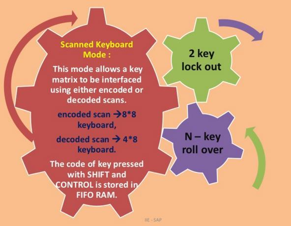
49 The DMA controller is the sole master of the bus, till the DMA operation is over. The CPU remains in the HOLD status (all of its signals are tristate except HOLD and HLDA), till the DMA controller is the master of the bus. In other words, the DMA controller interfacing circuit implements a switching arrangement for the address, data and control busses of the memory and peripheral subsystem from/to the CPU to/from the DMA controller. 4. Explain the operating Modes of (CO3-K2) Operating Modes 8279 provides three input modes, they are: Input Modes: 1. Scanned Keyboard Mode: This mode allows a key matrix to be interfaced using either encoded or decoded scans. In the encoded scan, an 8 x 8 keyboard or in decoded scan, a 4 x 8 Keyboard can be interfaced. The code of key pressed with SHIFT and CONTROL status is stored into the FIFO RAM. 49

50 50

51 In scanned keyboard mode with two key lockout, when a key is pressed debounce logic comes into operation. During the next two scans, the other keys are checked for closures and no other key is pressed, the first key is taken into consideration. The key code of the key pressed along with the SHIFT and CNTL status is entered into the FIFO if it is not full. If the FIFO is full, then the data will not be entered and an error flag is set. In scanned keyboard with N-key rollover, each key depression is treated independently. When a key is pressed, the debounce circuit waits for two keyboard scans and then checks whether the key is still depressed. If it is still depressed, the code is entered in FIFO. Any number of keys can be pressed simultaneously and recognized in the order, the keyboard scan recorded them. All the codes of such keys are entered into the FIFO. 2. Scanned Sensor Matrix: In this mode, a sensor array can be interfaced with 8279 using either encoder or decoder scans. With encoder scan 8 x 8 sensor matrix or with decoder scan 4 x 8 sensor matrix can be interfaced. The sensor codes are stored in the CPU addressable sensor RAM. 51
52 3. Strobed Input : In this mode, if the control line goes low, the data on return lines, is stored in the FIFO byte by byte. Output (Display) Modes : 8279 provides two output modes for selecting the display options. 1. Display Scan: In this mode, 8279 provides 8 or 16 character multiplexed displays those can be organized as dual 4-bit or single 8-bit display units. 2. Display Entry: The Display data is entered for display either from the right side or from the left side. Display Modes There are various options of data display. The first one is known as left entry mode or type writer mode. Since in a type writer the first character typed appears at the left-most position, while the subsequent characters appears successively to the right of the first one. The other display format is known as right entry mode, or calculator mode, since the calculator the first character entered appears at the right-most position and this character is shifted one position left when the next character is entered. 1. Left Entry Mode In the Left entry mode, the data is entered from the left side of the display unit. Address0 of the display RAM contains the leftmost display character and address 15 of the RAM contains the rightmost display character. 2. Right Entry Mode In the right entry mode, the first entry to be displayed is entered on the rightmost display.the next entry is also placed in the right most display but after the previous display is shifted left by one display position. ***** Unit 4 1. Explain in detail about PORT 0 in I/O and external memory interfacing. (CO4- K2) PORT 0 INPUTS 52
53 Step 1: The input of latch ie D=1 for input operation and the control signal should be zero for input/output operation, and it should be one to act as external memory. Step 2: The data (D=1) is available on Q if clock is activated. The Q signal is allowed to go through 2:1 Multiplexer. Since the control signal value is zero, it allows Q value on its output ( multiplexer). If it s one, the signal Add/data will be available on the output line of Multiplexer. Step 3: The input of Lower FET is zero, so it acts as an open circuit. And it doesn t allow anything to pass. Similarly the inputs of upper FET also zero, since one of the input of AND gate is zero. Finally both FET s won t allow anything to pass on it. Step 4: The voltage in-between the FET is in high impedance state. Because this point is neither connected to zero and nor connected to one. Now, port 0 is ready to act as input port. Suppose if any external device wants to write (zero or one), it will be available on buffer. PORT 0 AS OUTPUT To make output as 0 53
54 Step 1: The data (D=0) is available on Q if clock is activated. The Q = 1 signal is allowed to go through 2:1 Multiplexer. Since the control signal value is zero, it allows Q value on its output (multiplexer). If it s one, the signal Add/data will be available on the output line of Multiplexer. Step 2: The input of Lower FET is one, so it acts as a closed circuit. The one of the input of upper FET is zero, since one of the input of AND gate is zero. Finally the upper FET act as open circuit and the lower FET will act as closed circuit. Now the port will act as output Port. Step 3: The voltage in-between the FET is zero. Because, this point is connected to ground through lower FET. Now, port 0 is ready to act as output port. To make output as 1 Step 1: The data (D=1) is available on Q if clock is activated. The Q signal is allowed to go through 2:1 Multiplexer. Since the control signal value is zero, it allows Q value on its output ( multiplexer). 54
55 Step 2: The input of Lower FET is zero, so it acts as an open circuit. And it doesn t allow anything to pass. Similarly the inputs of upper FET also zero, since one of the input of AND gate is zero. Finally both FET s won t allow anything to pass on it. Step 3: The voltage in-between the FET is in high impedance state. Because this point is neither connected to zero and nor connected to one. To get one in this point, pull up resistor is connected across upper FET. Now the value is one at this point Note: Pull up resistor is capable of setting the vaule to one, if its previous value is in high impedance state. Port 0 as External Memory To get output as zero Step 1: Control signal and Address/Data bit is set to be one. The value on Add/Data will be available on the output of Mux 2:1. Now the lower FET acts as open switch and the upper FET acts as closed switch. The value at the junction point is one. Since the point is connected to Vcc through upper FET. To get output as one 55
56 Step 1: Control signal is set to be one and Address/Data bit is set to be zero. The value on Add/Data will be available on the output of Mux 2:1. Now the lower FET acts as closed switch and the upper FET acts as open switch. The value at the junction point is zero. Since the point is connected to ground through lower FET. ***** 2. Explain the architecture of (CO4-K2) 56
57 Features: 8-bit CPU 16-bit Program Counter 8-bit Processor Status Word (PSW) 8-bit Stack Pointer Internal RAM of 128bytes Special Function Registers (SFRs) of 128 bytes 32 I/O pins arranged as four 8-bit ports (P0 - P3) Two 16-bit timer/counters : T0 and T1 Two external and three internal vectored interrupts One full duplex serial I/O The heart of 8051 is the circuitry that generates the clock pulses by which all internal operations are synchronised. Pins XTAL1 and XTAL2 are provided for connecting resonator to form an oscillator. The time taken to complete any instruction is called as machine cycle or instruction cycle. In 8051 one instruction cycle consists of 6 states or 12 clock cycles, instruction cycle is also referred as Machine cycle. 57
58 Instruction cycle of 8051 (Instruction cycle has six states (S 1 - S 6 ). Each state has two pulses (P1 and P2)) 128 bytes of Internal RAM Structure The lower 32 bytes are divided into 4 separate banks. Each register bank has 8 registers of one byte each. A register bank is selected depending upon two bank select bits in the PSW register. (RS1,RS0 bits of PSW) Next 16bytes are bit addressable. In total, 128bits (16X8) are available in bit addressable area. Each bit can be accessed and modified by suitable instructions.a bit variable can be set with a command such as SETB and cleared with a command such as CLR. Example instructions are: SETB 25h ; sets the bit 25h (becomes 1) CLR 25h ; clears bit 25h (becomes 0) The bit addresses are from 00H (LSB of the first byte in 20H) to 7FH (MSB of the last byte in 2FH). Remaining 80bytes of RAM are available for general purpose. The general purpose RAM can be accessed using direct or indirect addressing modes. Internal Data Memory and Special Function Register (SFR) Map 58

59 The special function registers (SFRs) are mapped in the upper 128 bytes of internal data memory address. Hence there is an address overlap between the upper 128 bytes of data RAM and SFRs. Note that the upper 128 bytes of data RAM are present only in the 8052 family. The lower128 bytes of RAM (00H - 7FH) can be accessed both by direct or indirect addressing while the upper 128 bytes of RAM (80H - FFH) are accessed by indirect addressing. The SFRs (80H - FFH) are accessed by direct addressing only. This feature distinguishes the upper 128 bytes of memory from the SFRs, as shown in figure. The set of Special Function Registers (SFRs) contains important registers such as Accumulator, Register B, I/O Port latch registers, Stack pointer, Data Pointer, Processor Status Word (PSW) and various control registers. Processor Status Word (PSW) 59

60 Accumulator is an 8 bit register widely used for all arithmetic and logical operations. Accumulator is also used to transfer data between external memory. B register is used along with Accumulator for multiplication and division. A and B registers together is also called MATH registers. Stack Pointer (SP) it contains the address of the data item on the top of the stack. Stack may reside anywhere on the internal RAM. On reset, SP is initialized to 07 so that the default stack will start from address 08 onwards. Data Pointer (DPTR) DPH (Data pointer higher byte), DPL (Data pointer lower byte). This is a 16 bit register which is used to furnish address information for internal and external program memory and for external data memory. Program Counter (PC) 16 bit PC contains the address of next instruction to be executed. On reset PC will set to After fetching every instruction PC will increment by one. 3. Explain the following addressing modes of 8051 with an Example. (CO4-K2) 1. Immediate addressing, 2. Register addressing, 3. Direct addressing, 4. Indirect addressing, 5. Relative addressing. 1. Immediate addressing. In this addressing mode the data is provided as a part of instruction itself. In other words data immediately follows the instruction. Eg. MOV A,#30H ADD A, #83 # Symbol indicates the data is immediate. 60
61 2. Register addressing. In this addressing mode the register will hold the data. One of the eight general registers (R0 to R7) can be used and specified as the operand. Eg. MOV A,R0 ADD A,R6 R0 R7 will be selected from the current selection of register bank. The default register bank will be bank Direct addressing There are two ways to access the internal memory. Using direct address and indirect address. Using direct addressing mode we can not only address the internal memory but SFRs also. In direct addressing, an 8 bit internal data memory address is specified as part of the instruction and hence, it can specify the address only in the range of 00H to FFH. In this addressing mode, data is obtained directly from the memory. Eg. MOV A,60h ADD A,30h 4. Direct addressing There are two ways to access the internal memory. Using direct address and indirect address. Using direct addressing mode we can not only address the internal memory but SFRs also. In direct addressing, an 8 bit internal data memory address is specified as part of the instruction and hence, it can specify the address only in the range of 00H to FFH. In this addressing mode, data is obtained directly from the memory. Eg. MOV A,60h ADD A,30h 5. Indexed addressing. In indexed addressing, either the program counter (PC), or the data pointer (DTPR) is used to hold the base address, and the A is used to hold the offset address. Adding the value of the base address to the value of the offset address forms the effective address. Indexed addressing is used with JMP or MOVC instructions. Look up tables are easily implemented with the help of index addressing. Eg. MOVC // copies the contents of memory location pointed by the sum of the accumulator A and the DPTR into accumulator A. MOVC // copies the contents of memory location pointed by the sum of the accumulator A and the program counter into accumulator A. 4. Explain the following addressing modes of 8051 with an Example. (CO4-K2) 61
62 1. Absolute addressing, 2. Long addressing 3. Indexed addressing, 4. Bit inherent addressing, 5. Bit direct addressing. 1. Relative Addressing. Relative addressing is used only with conditional jump instructions. The relative address, (offset), is an 8 bit signed number, which is automatically added to the PC to make the address of the next instruction. The 8 bit signed offset value gives an address range of +127 to 128 locations. The jump destination is usually specified using a label and the assembler calculates the jump offset accordingly. The advantage of relative addressing is that the program code is easy to relocate and the address is relative to position in the memory. Eg. SJMP LOOP1 2. Absolute addressing Absolute addressing is used only by the AJMP (Absolute Jump) and ACALL (Absolute Call) instructions. These are 2 bytes instructions. The absolute addressing mode specifies the lowest 11 bit of the memory address as part of the instruction. The upper 5 bit of the destination address are the upper 5 bit of the current program counter. Hence, absolute addressing allows branching only within the current 2 Kbyte page of the program memory. Eg. AJMP LOOP1 ACALL LOOP2 3. Long Addressing The long addressing mode is used with the instructions LJMP and LCALL. These are 3 byte instructions. The address specifies a full 16 bit destination address so that a jump or a call can be made to a location within a 64 Kbyte code memory space. Eg. LJMP FINISH LCALL DELAY 4. Bit Inherent Addressing In this addressing, the address of the flag which contains the operand, is implied in the opcode of the instruction. Eg. CLR C ; Clears the carry flag to 0 5. Bit Direct Addressing In this addressing mode the direct address of the bit is specified in the instruction. The RAM space 20H to 2FH and most of the special function registers are bit addressable. Bit address values are between 00H to 7FH. Eg. CLR 07h ; Clears the bit 7 of 20h RAM space 62
 Timer Timers/Counters are used generally for Time reference Creating delay Wave form properties measurement Periodic interrupt generation Waveform generation The two timers in 8051 share two")
63 SETB 07H ; Sets the bit 7 of 20H RAM space. Unit 5 1. Show the structure of registers in Timer and Counter of (CO5-K2) Timer Timers/Counters are used generally for Time reference Creating delay Wave form properties measurement Periodic interrupt generation Waveform generation The two timers in 8051 share two SFRs (TMOD and TCON) which control the timers, and each timer also has two SFRs dedicated solely to itself (TH0/TL0 and TH1/TL1) has two 16-bit programmable UP timers/counters. They can be configured to operate either as timers or as event counters In the "timer" function mode, the counter is incremented in every machine cycle. In the "counter" function mode, the register is incremented in response to a 1 to 0 transition at its corresponding external input pin (T0 or T1). It requires 2 machine cycles to detect a high to low transition. 1.1.Timer Mode control (TMOD) Special Function Register Gate: Based on the status of the signal. Timer starts counting using either internal clock (timer mode) or external pulses (counter mode). C/T*: It is used for the selection of Counter/Timer mode. Mode Select Bits: 1.2. Timer control (TCON) Special function register: TCON is bit addressable. The address of TCON is 88H. It is partly related to Timer and partly to interrupt. 63

64 2. Interrupt 8051 has five interrupts. They are maskable and vectored interrupts. Out of these five, two are external interrupt and three are internal interrupts makes use of two registers to deal with interrupts. 64
65 2.1. IE Register - Interrupt Enable register This is an 8 bit register used for enabling or disabling the interrupts. The structure of IE is 2.2. IP Register. This is an 8 bit register used for setting the priority of the interrupts. 2. Demonstrate the interfacing keyboard and display with (C05-K2) Keyboards and LCDs are the most widely used input/output devices of the Interfacing the keyboard to the
66 Keyboards are organized in a matrix of rows and columns. The CPU accesses both rows and columns through ports; therefore, with two 8-bit ports, an 8 x 8 matrix of keys can be connected to a microprocessor. When a key is pressed, a row and a column make a contact; otherwise, there is no connection between rows and columns. In IBM PC keyboards, a single microcontroller (consisting of a microprocessor, RAM and EPROM, and several ports all on a single chip) takes care of hardware and software interfacing of the keyboard. In such systems, it is the function of programs stored in the EPROM of the microcontroller to scan the keys continuously, identify which one has been activated, and present it to the motherboard. Scanning and identifying the key Figure shows a 4 x 4 matrix connected to two ports. The rows are connected to an output port and the columns are connected to an input port. If no key has been pressed, reading the input port will yield 1 s for all columns since they are all connected to high (Vcc). If all the rows are grounded and a key is pressed, one of the columns will have 0 since the key pressed provides the path to ground. It is the function of the microcontroller to scan the keyboard continuously to detect and identify the key pressed. 66
67 Matrix Keyboard Connection to Ports To detect a pressed key, the microcontroller grounds all rows by providing 0 to the output latch, then it reads the columns. If the data read from the columns is D3 DO = 1111, no key has been pressed and the process continues until a key press is detected. However, if one of the column bits has a zero, this means that a key press has occurred. For example, if D3 DO = 1101, this means that a key in the Dl column has been pressed. After a key press is detected, the microcontroller will go through the process of identifying the key. Starting with the top row, the microcontroller grounds it by providing a low to row DO only; then it reads the columns. If the data read is all 1 s, no key in that row is activated and the process is moved to the next row. It grounds the next row, reads the columns, and checks for any zero. This process continues until the row is identified. Example 12-3 From Figure, identify the row and column of the pressed key for each of the following. D3 DO = 1110 for the row, D3 DO = 1011 for the column D3 DO = 1101 for the row, D3 DO = 0111 for the column Solution: From Figure the row and column can be used to identify the key. The row belongs to DO and the column belongs to D2; therefore, key number 2 was pressed. The row belongs to Dl and the column belongs to D3; therefore, key number 7 was pressed. Interfacing hex keypad to 8051 The circuit is very simple and it uses only two ports of the microcontroller, one for the hex keypad and the other for the seven segment LED display 67
68 The hex keypad is interfaced to port 1 and seven segment LED display is interfaced to port 0 of the microcontroller. Resistors R1 to R8 limits the current through the corresponding segments of the LED display. Capacitors C1, C2 and crystal X1 completes the clock circuitry for the microcontroller. Capacitor C3, resistor R9 and push button switch S1 forms a debouncing reset mechanism. Note: The hardware designer has to select keys that will survive in the intended environment. The programmer must write the code that will anticipate and defeat deliberate attempts by human to confuse program. The software must be such that the keyboard application must guard against following Human Factors: 1. More than one key pressed. 2. Key pressed and held. 3. Rapid key press and release. 5.2 Keyboard Configurations 3. Demonstrate the algorithm for programming Timers in (CO5-K2) 68
69 Mode 1: Load the TMOD value register indicating which timer (0 or 1) is to be used and which timer mode is selected. Load registers TL and TH with initial count values. Start the timer by the instruction SETB TR0 for timer 0 and SETB TR1 for timer 1. Keep monitoring the timer flag (TF) with the JNB TFx, target instruction to see if it is raised. Get out of the loop when TF becomes high. Stop the timer with the instructions CLR TR0 or CLR TR1, for timer 0 and timer 1, respectively. Clear the TF flag for the next round with the instruction CLR TF0 or CLR TF1, for timer 0 and timer 1, respectively. Go back to step 2 to load TH and TL again. Program: count value is FFO6 MOV TMOD,#10 ; Timer 1, mode 1 AGAIN: MOV TL1,#06H ; TL0 = 06H MOV TH1,#0FFH ; TH0 = FFH SETB TR1 ; Start timer 1 BACK: JNB TF1,BACK ; Stay until timer rolls over CLR TR1 ; Stop timer 1 CPL P1.5 ; Complement P1.5 to get Hi, Lo CLR TF1 ; Clear timer flag 1 SJMP AGAIN ; Reload timer Mode 0: The programming techniques mentioned here are also applicable to counter/timer mode 0. The only difference is in the number of bits of the initialization value. Mode 2: Load the TMOD value register indicating which timer (0 or 1) is to be used; select timer mode 2. Load TH register with the initial count value. As it is an 8-bit timer, the valid range is from 00 to FFH. Start the timer. Keep monitoring the timer flag (TFx) with the JNB TFx, target instruction to see if it is raised. Get out of the loop when TFx goes high. Clear the TFx flag. Go back to step 4, since mode 2 is auto-reload. 69
70 4. 5. Explain interfacing of stepper motor with (CO5- K2) Stepper Motor Interfacing: Stepper motor is a widely used device that translates electrical pulses into mechanicalmovement. Stepper motor is used in applications such as; disk drives, dot matrix printer,robotics etc. The construction of the motor is as shown in figure.. Structure of stepper motor It has a permanent magnet rotor called the shaft which is surrounded by a stator. Commonlyused stepper motors have four stator windings that are paired with a center tapped common. Such motors are called as four-phase or unipolar stepper motor. The stator is a magnet over which the electric coil is wound. One end of the coil are connected commonly either to ground or +5V. The other end is provided with a fixed sequence such that the motor rotates in a particular direction. Stepper motor shaft moves in a fixed repeatable increment, which allows one to move it to a precise position. Direction of the rotation is dictated by the stator poles. Stator poles are determined by the current sent through the wire coils. Step angle: Step angle is defined as the minimum degree of rotation with a single step No of steps per revolution = 360 / step angle Steps per second = (rpm x steps per revolution) / 60 Example: step angle = 2 No of steps per revolution =
71 Switching Sequence of Motor: As discussed earlier the coils need to be energized for the rotation. This can be done by sending a bits sequence to one end of the coil while the other end is commonly connected. The bit sequence sent can make either one phase ON or two phase ON for a full step sequence or it can be a combination of one and two phase ON for half step sequence. Both are tabulated below. Full step sequence: Two coils are energized at the same time and motor shaft rotates. The order in which the coils has to be energized is given in the table. Two Phase ON One Phase ON Halfstep : In half steps sequence, motor step angle reduces to half the angle in full mode. So the angular resolution is also increased, it becomes double the angular resolution. Also in half mode sequence the number of steps gets doubled as that of full mode. 71
72 Components: 8051, Stepper motor 6 pins and Stepper motor driver Motor is connected to the port2 of the microcontroller through a driver IC. The ULN2003A is a current driver IC. It is used to drive the current of the stepper motor as it requires more than 60mA of current. It is an array of Darlington pairs. It consists of seven pairs of Darlington arrays with common emitter. The IC consists of 16 pins in which 7 are input pins, 7 are output pins and remaining are VCC and Ground. The first four input pins are connected to the microcontroller. In the same way, four output pins are connected to the stepper motor. Stepper motor has 6 pins. In these six pins, 2 pins are connected to the supply of 12V and the remaining are connected to the output of the stepper motor. Stepper rotates at a given step angle. Each step in rotation is a fraction of full cycle. This depends on the mechanical parts and the driving method. PART C - Descriptive Questions: (8 Marks) 1. Develop an assembly language program to perform 8 bit addition, subtraction, Multiplication and division with neat flowchart using 8051 instruction set. (CO4-K2) 2. Show the status of stack after executing PUSH and POP instruction. (CO1-K2) 72
73 STACK The stack is a block of memory that may be used for temporarily storing the contents of the registers inside the CPU. When the information is written on the stack, the operation is called PUSH. When the information is read from stack, the operation is called a POP. The stack is essentially Last-In-First-Out (LIFO) data segment. This means that the data which is pushed into the stack last will be on top of stack and will be popped off the stack first. This stack is implemented with the help of special memory pointer register. The special pointer register is called the stack pointer. During push and pop operation, stack pointer register gives the address of memory where the information is to be stored or to be read. The memory location currently pointed by stack pointer is called as top of stack. The stack pointer is a 16-bit register that contains the offset address of the memory location in the stack segment. For stack operation, physical address is produced by adding the contents of stack pointer register to the segment base address in SS.To find physical address, contents of the stack segment register are shifted four bits left and the contents of SP are added to the shifted result. If the contents of SP are 2050H and SS are 5000H then the physical address is calculated as follows: SS H SP H PA H PUSH OPERATION The Fig shows the map of the stack before and after execution of PUSH AX and PUSH CX instruction. Examples: PUSH CX - Decremented SP by 2, Copy CX to stack t 73
74 POP OPERATION The POP instruction copies a word from the stack location pointed by the stack pointer to the destinations. The destination can be a general purpose register, a segment register or a memory location. The stack pointer is automatically incremented by 2 after the word is copied to the specified destination. Example 1. POP DS - copy a word from top of stack to DS and increment SP by POP CX Copy a word form top of stack to CX and increment SP by Show the timing diagram for general bus operation. (CO2-K2) General Bus Operation: Basic configurations 74
75 The 8086 has a combined address and data bus commonly referred as a time multiplexed address and data bus. The main reason behind multiplexing address and data over the same pins is the maximum utilization of processor pins and it facilitates the use of 40 pin standard DIP package. The bus can be demultiplexed using a few latches and transceivers, whenever required. Basically, all the processor bus cycles consist of at least four clock cycles. These are referred to as T1, T2, T3, T4. The address is transmitted by the processor during T1, It is present on the bus only for one cycle. The negative edge of this ALE pulse is used to separate the address and the data or status information. The ALE signal is used activate latches and thus to latch the address. The data transfer occurs on the bus during T3and T4. The time interval T2 is used for changing the direction of the bus during read operations. Ready signal is sampled during T3. The slower peripheral devices use this signal to indicate that the device is not ready to send the desired data within specified time. Not ready indication is given by the slower peripheral device. Wait state TW is inserted in between T2 and T3 to give enough access time for the slower peripheral devices. Each wait state is of the same as a clock cycle. During this wait state, the signals on the buses remain the same as they were at the start of the WAIT state. During WAIT state, if the Ready signal input is high then after the 8086 will go on with the regular T4 of the machine cycle. If the Ready input is low at the end of a WAIT state, then 8086 insert another WAIT state until the Ready input is made high again. In maximum mode, the status lines S0, S1 and S2 are used to indicate the type of operation. 75

76 Status bits S3 to S7 are multiplexed with higher order address bits and the BHE signal. Address is valid during T1 while status bits S3 to S7 are valid during T2 through T4. 4. Explain the different modes of operation of 8253/54 timer. (CO3-K2) 76


77 77

78 78
79 5. Explain interfacing of stepper motor with (CO5-K2) Stepper Motor Interfacing: Stepper motor is a widely used device that translates electrical pulses into mechanicalmovement. Stepper motor is used in applications such as; disk drives, dot matrix printer,robotics etc. The construction of the motor is as shown in figure.. 79

80 Structure of stepper motor It has a permanent magnet rotor called the shaft which is surrounded by a stator. Commonlyused stepper motors have four stator windings that are paired with a center tapped common. Such motors are called as four-phase or unipolar stepper motor. The stator is a magnet over which the electric coil is wound. One end of the coil are connected commonly either to ground or +5V. The other end is provided with a fixed sequence such that the motor rotates in a particular direction. Stepper motor shaft moves in a fixed repeatable increment, which allows one to move it to a precise position. Direction of the rotation is dictated by the stator poles. Stator poles are determined by the current sent through the wire coils. Step angle: Step angle is defined as the minimum degree of rotation with a single step No of steps per revolution = 360 / step angle Steps per second = (rpm x steps per revolution) / 60 Example: step angle = 2 No of steps per revolution = 180 Switching Sequence of Motor: As discussed earlier the coils need to be energized for the rotation. This can be done by sending a bits sequence to one end of the coil while the other end is commonly connected. The bit sequence sent can make either one phase ON or two phase ON for a full step sequence or it can be a combination of one and two phase ON for half step sequence. Both are tabulated below. Full step sequence: Two coils are energized at the same time and motor shaft rotates. The order in which the coils has to be energized is given in the table. 80

81 Two Phase ON One Phase ON Halfstep : In half steps sequence, motor step angle reduces to half the angle in full mode. So the angular resolution is also increased, it becomes double the angular resolution. Also in half mode sequence the number of steps gets doubled as that of full mode. 81

82 Components: 8051, Stepper motor 6 pins and Stepper motor driver Motor is connected to the port2 of the microcontroller through a driver IC. The ULN2003A is a current driver IC. It is used to drive the current of the stepper motor as it requires more than 60mA of current. It is an array of Darlington pairs. It consists of seven pairs of Darlington arrays with common emitter. The IC consists of 16 pins in which 7 are input pins, 7 are output pins and remaining are VCC and Ground. The first four input pins are connected to the microcontroller. In the same way, four output pins are connected to the stepper motor. Stepper motor has 6 pins. In these six pins, 2 pins are connected to the supply of 12V and the remaining are connected to the output of the stepper motor. Stepper rotates at a given step angle. Each step in rotation is a fraction of full cycle. This depends on the mechanical parts and the driving method. 82
Question Bank Microprocessor and Microcontroller
 QUESTION BANK - 2 PART A 1. What is cycle stealing? (K1-CO3) During any given bus cycle, one of the system components connected to the system bus is given control of the bus. This component is said to
UNIT II OVERVIEW MICROPROCESSORS AND MICROCONTROLLERS MATERIAL. Introduction to 8086 microprocessors. Architecture of 8086 processors
 OVERVIEW UNIT II Introduction to 8086 microprocessors Architecture of 8086 processors Register Organization of 8086 Memory Segmentation of 8086 Pin Diagram of 8086 Timing Diagrams for 8086 Interrupts of
VARDHAMAN COLLEGE OF ENGINEERING (AUTONOMOUS) Shamshabad, Hyderabad
 Shamshabad, Hyderabad") Introduction to MS-DOS Debugger DEBUG In this laboratory, we will use DEBUG program and learn how to: 1. Examine and modify the contents of the 8086 s internal registers, and dedicated parts of the memory
Introduction to MS-DOS Debugger DEBUG In this laboratory, we will use DEBUG program and learn how to: 1. Examine and modify the contents of the 8086 s internal registers, and dedicated parts of the memory
Introduction to Microprocessor
 Introduction to Microprocessor The microprocessor is a general purpose programmable logic device. It is the brain of the computer and it performs all the computational tasks, calculations data processing
EC 6504 Microprocessor and Microcontroller. Unit II System Bus Structure
 EC 6504 Microprocessor and Microcontroller Unit II 8086 System Bus Structure Syllabus: 8086 Signals Basic Configurations System bus timing System Design using 8086 IO Programming Introduction to multiprogramming
8086 INTERNAL ARCHITECTURE
 8086 INTERNAL ARCHITECTURE Segment 2 Intel 8086 Microprocessor The 8086 CPU is divided into two independent functional parts: a) The Bus interface unit (BIU) b) Execution Unit (EU) Dividing the work between
 UNIT II SYSTEM BUS STRUCTURE 1. Differentiate between minimum and maximum mode 2. Give any four pin definitions for the minimum mode. 3. What are the pins that are used to indicate the type of transfer
Intel 8086 MICROPROCESSOR. By Y V S Murthy
 Intel 8086 MICROPROCESSOR By Y V S Murthy 1 Features It is a 16-bit μp. 8086 has a 20 bit address bus can access up to 2 20 memory locations (1 MB). It can support up to 64K I/O ports. It provides 14,
UNIT-1. It is a 16-bit Microprocessor (μp).it s ALU, internal registers works with 16bit binary word.
.it s ALU, internal registers works with 16bit binary word.") UNIT-1 Introduction to 8086: 8086 Microprocessor is an enhanced version of 8085Microprocessor that was designed by Intel in 1976. It is a 16-bit Microprocessor having 20 address lines and16 data lines
UNIT-1 Introduction to 8086: 8086 Microprocessor is an enhanced version of 8085Microprocessor that was designed by Intel in 1976. It is a 16-bit Microprocessor having 20 address lines and16 data lines
9/25/ Software & Hardware Architecture
 8086 Software & Hardware Architecture 1 INTRODUCTION It is a multipurpose programmable clock drive register based integrated electronic device, that reads binary instructions from a storage device called
Unit I Introduction. Department of Electronics and Communication Engineering VARDHAMAN COLLEGE OF ENGINEERING Shamshabad, Hyderabad , India.
 Unit I Introduction Department of Electronics and Communication Engineering VARDHAMAN COLLEGE OF ENGINEERING Shamshabad, Hyderabad 501218, India. Pre-requisites Digital Logic Design (A1404) Computer Architecture
icroprocessor istory of Microprocessor ntel 8086:
 Microprocessor A microprocessor is an electronic device which computes on the given input similar to CPU of a computer. It is made by fabricating millions (or billions) of transistors on a single chip.
MICROPROCESSOR PROGRAMMING AND SYSTEM DESIGN
 MICROPROCESSOR PROGRAMMING AND SYSTEM DESIGN ROAD MAP SDK-86 Intel 8086 Features 8086 Block Diagram 8086 Architecture Bus Interface Unit Execution Unit 8086 Architecture 8086 Programmer s Model Flag Register
UNIT-I. 1.Draw and explain the Architecture of a 8085 Microprocessor?
 UNIT-I INTRODUCTION TO MICROPROCESSOR A common way of categorizing microprocessors is by the no. of bits that their ALU can work with at a time. (i) The first commercially available microprocessor was
Lecture 5:8086 Outline: 1. introduction 2. execution unit 3. bus interface unit
 Lecture 5:8086 Outline: 1. introduction 2. execution unit 3. bus interface unit 1 1. introduction The internal function of 8086 processor are partitioned logically into processing units,bus Interface Unit(BIU)
UNIT 1. Introduction to microprocessor. Block diagram of simple computer or microcomputer.
 UNIT 1 Unit 1 contents at a glance: 1. Architecture of 8086 microprocessor, 2. Register organization, 3. 8086 flag register and its functions, 4. addressing modes of 8086, 5. Pin diagram of 8086, 6. Minimum
Intel 8086 MICROPROCESSOR ARCHITECTURE
 Intel 8086 MICROPROCESSOR ARCHITECTURE 1 Features It is a 16-bit μp. 8086 has a 20 bit address bus can access up to 2 20 memory locations (1 MB). It can support up to 64K I/O ports. It provides 14, 16
Internal architecture of 8086
 Case Study: Intel Processors Internal architecture of 8086 Slide 1 Case Study: Intel Processors FEATURES OF 8086 It is a 16-bit μp. 8086 has a 20 bit address bus can access up to 220 memory locations (1
SRI VENKATESWARA COLLEGE OF ENGINEERING AND TECHNOLOGY DEPARTMENT OF ECE EC6504 MICROPROCESSOR AND MICROCONTROLLER (REGULATION 2013)
") SRI VENKATESWARA COLLEGE OF ENGINEERING AND TECHNOLOGY DEPARTMENT OF ECE EC6504 MICROPROCESSOR AND MICROCONTROLLER (REGULATION 2013) UNIT I THE 8086 MICROPROCESSOR PART A (2 MARKS) 1. What are the functional
SRI VENKATESWARA COLLEGE OF ENGINEERING AND TECHNOLOGY DEPARTMENT OF ECE EC6504 MICROPROCESSOR AND MICROCONTROLLER (REGULATION 2013) UNIT I THE 8086 MICROPROCESSOR PART A (2 MARKS) 1. What are the functional
EC 6504 MICROPROCESSOR AND MICROCONTROLLER Electronicsand Communication Engineering Fifth Semester UNIT-1I Part A 1. Definemachinecycle.
 EC 6504 MICROPROCESSOR AND MICROCONTROLLER Electronicsand Communication Engineering Fifth Semester UNIT-1I Part A 1. Definemachinecycle. [N/D 16] Machine cycle is defined as the time required to complete
UNIT 2 PROCESSORS ORGANIZATION CONT.
 UNIT 2 PROCESSORS ORGANIZATION CONT. Types of Operand Addresses Numbers Integer/floating point Characters ASCII etc. Logical Data Bits or flags x86 Data Types Operands in 8 bit -Byte 16 bit- word 32 bit-
8086 PIN Diagram Signals with common functions in both Modes: The following signal description is common for both the minimum and maximum modes.
 UNIT II - 8086 SYSTEM BUS STRUCTURE 8086 signals Basic configurations System bus timing System design using 8086 IO programming Introduction to Multiprogramming System Bus Structure Multiprocessor configurations
Microprocessor. By Mrs. R.P.Chaudhari Mrs.P.S.Patil
 Microprocessor By Mrs. R.P.Chaudhari Mrs.P.S.Patil Chapter 1 Basics of Microprocessor CO-Draw Architecture Of 8085 Salient Features of 8085 It is a 8 bit microprocessor. It is manufactured with N-MOS technology.
SRI VIDYA COLLEGE OF ENGINEERING AND TECHNOLOGY,VIRUDHUNAGAR
 Year/sem: 02/04 Academic Year: 2014-2015 (even) UNIT II THE 8086 SYSTEM BUS STRUCTURE PART A 1. What are the three groups of signals in 8086? The 8086 signals are categorized in three groups. They are:
INTRODUCTION TO MICROPROCESSORS
 INTRODUCTION TO MICROPROCESSORS Richa Upadhyay Prabhu NMIMS s MPSTME richa.upadhyay@nmims.edu January 7, 2016 Richa Upadhyay Prabhu (MPSTME) INTRODUCTION January 7, 2016 1 / 63 Course Design Prerequisite:
WINTER 12 EXAMINATION Subject Code : Model Answer Page No : / N. a) Describe the function of SID and SOD pins of 8085 microprocessor
 Describe the function of SID and SOD pins of 8085 microprocessor") Subject Code : Model Answer Page No : / N Q.1) SOLVE ANY FIVE : (20 MARKS) a) Describe the function of SID and SOD pins of 8085 microprocessor Ans: - SID: - (2 Mark) Serial Input Data SID pin is used to
Subject Code : Model Answer Page No : / N Q.1) SOLVE ANY FIVE : (20 MARKS) a) Describe the function of SID and SOD pins of 8085 microprocessor Ans: - SID: - (2 Mark) Serial Input Data SID pin is used to
Lecture 5: Computer Organization Instruction Execution. Computer Organization Block Diagram. Components. General Purpose Registers.
 Lecture 5: Computer Organization Instruction Execution Computer Organization Addressing Buses Fetch-Execute Cycle Computer Organization CPU Control Unit U Input Output Memory Components Control Unit fetches
EC6504 MICROPROCESSOR AND MICROCONTROLLER
 UNIT I THE 8086 MICROPROCESSOR 1. What do you mean by Addressing modes? (May/June 2014) The different ways that a microprocessor can access data are referred to as addressing modes. 2. What is meant by
 Question Bank Part-A UNIT I- THE 8086 MICROPROCESSOR 1. What is microprocessor? A microprocessor is a multipurpose, programmable, clock-driven, register-based electronic device that reads binary information
Topic 2 :16 Bit Microprocessor: 8086 (24 Marks)
") Topic 2 :16 Bit Microprocessor: 8086 (24 Marks) Features of 8086 8086 is a 16 bit processor. It s ALU, internal registers works with 16bit binary word 8086 has a 16bit data bus. It can read or write data
Topic 2 :16 Bit Microprocessor: 8086 (24 Marks) Features of 8086 8086 is a 16 bit processor. It s ALU, internal registers works with 16bit binary word 8086 has a 16bit data bus. It can read or write data
A Presentation created By Ramesh.K Press Ctrl+l for full screen view
 Press Ctrl+l for full screen view A Presentation created By Ramesh.K rameshpkd@gmail.com Press Ctrl+l for full screen view A Microprocessor sor is a multipurpose, programmable logic device that reads binary
1 MALP ( ) Unit-1. (1) Draw and explain the internal architecture of 8085.
 Unit-1. (1) Draw and explain the internal architecture of 8085.") (1) Draw and explain the internal architecture of 8085. The architecture of 8085 Microprocessor is shown in figure given below. The internal architecture of 8085 includes following section ALU-Arithmetic
(1) Draw and explain the internal architecture of 8085. The architecture of 8085 Microprocessor is shown in figure given below. The internal architecture of 8085 includes following section ALU-Arithmetic
CC411: Introduction To Microprocessors
 CC411: Introduction To Microprocessors OBJECTIVES this chapter enables the student to: Describe the Intel family of microprocessors from 8085 to Pentium. In terms of bus size, physical memory & special
ELE 3230 Microprocessors and Computer Systems
 ELE 3230 Microprocessors and Computer Systems Chapter 4 8088 System Architecture (*Hall:ch2; Brey:ch1; Triebel:ch2) ELE 3230 - Chapter 4 1 Historical Background 1969/70 Intel 4004, first Microprocessor
EC2304-MICROPROCESSOR AND MICROCONROLLERS 2 marks questions and answers UNIT-I
 EC2304-MICROPROCESSOR AND MICROCONROLLERS 2 marks questions and answers 1. Define microprocessors? UNIT-I A semiconductor device(integrated circuit) manufactured by using the LSI technique. It includes
1. INTRODUCTION TO MICROPROCESSOR AND MICROCOMPUTER ARCHITECTURE:
 1. INTRODUCTION TO MICROPROCESSOR AND MICROCOMPUTER ARCHITECTURE: A microprocessor is a programmable electronics chip that has computing and decision making capabilities similar to central processing unit
1. What is Microprocessor? Give the power supply & clock frequency of 8085?
 1. What is Microprocessor? Give the power supply & clock frequency of 8085? A microprocessor is a multipurpose, programmable logic device that reads binary instructions from a storage device called memory
LECTURE NOTES MICROPROCESSORS AND INTERFACING DEVICES
 LECTURE NOTES ON MICROPROCESSORS AND INTERFACING DEVICES III B. Tech II semester (JNTUH-R15) Mr.R Mahendhar Reddy, Associate Professor, ECE ELECTRICAL AND ELECTRONICS ENGINEERING INSTITUTE OF AERONAUTICAL
Code segment Stack segment
 Registers Most of the registers contain data/instruction offsets within 64 KB memory segment. There are four different 64 KB segments for instructions, stack, data and extra data. To specify where in 1
1. Internal Architecture of 8085 Microprocessor
 1. Internal Architecture of 8085 Microprocessor Control Unit Generates signals within up to carry out the instruction, which has been decoded. In reality causes certain connections between blocks of the
Architecture of 8085 microprocessor
 Architecture of 8085 microprocessor 8085 consists of various units and each unit performs its own functions. The various units of a microprocessor are listed below Accumulator Arithmetic and logic Unit
Control Unit: The control unit provides the necessary timing and control Microprocessor resembles a CPU exactly.
 Unit I 8085 and 8086 PROCESSOR Introduction to microprocessor A microprocessor is a clock-driven semiconductor device consisting of electronic logic circuits manufactured by using either a large-scale
Microprocessor Architecture
 Microprocessor - 8085 Architecture 8085 is pronounced as "eighty-eighty-five" microprocessor. It is an 8-bit microprocessor designed by Intel in 1977 using NMOS technology. It has the following configuration
Northern India Engineering College, Delhi (GGSIP University) PAPER I
 PAPER I") PAPER I Q1.Explain IVT? ANS. interrupt vector table is a memory space for storing starting addresses of all the interrupt service routine. It stores CS:IP PAIR corresponding to each ISR. An interrupt vector
PAPER I Q1.Explain IVT? ANS. interrupt vector table is a memory space for storing starting addresses of all the interrupt service routine. It stores CS:IP PAIR corresponding to each ISR. An interrupt vector
8086 Microprocessors & Peripherals
 8086 Microprocessors & Peripherals (06IT/BM - 52) Sessions handled by Prof. M.V. SREENIVAS RAO. GSSSIETW, MYSORE Prof. M. SHIVAKUMAR. BIET, DAVANGERE Prof. VAGEESH.V.KANTLI. BIET, DAVANGERE 1 8086 MICROPROCESSOR
CHAPTER 5 : Introduction to Intel 8085 Microprocessor Hardware BENG 2223 MICROPROCESSOR TECHNOLOGY
 CHAPTER 5 : Introduction to Intel 8085 Hardware BENG 2223 MICROPROCESSOR TECHNOLOGY The 8085A(commonly known as the 8085) : Was first introduced in March 1976 is an 8-bit microprocessor with 16-bit address
Basic characteristics & features of 8086 Microprocessor Dr. M. Hebaishy
 Basic characteristics & features of 8086 Microprocessor Dr. M. Hebaishy Digital Logic Design Ch1-1 8086 Microprocessor Features: The 8086 microprocessor is a 16 bit microprocessor. The term 16 bit means
Unit DMA CONTROLLER 8257
 DMA CONTROLLER 8257 In microprocessor based system, data transfer can be controlled by either software or hardware. To transfer data microprocessor has to do the following tasks: Fetch the instruction
ADVANCE MICROPROCESSOR & INTERFACING
 VENUS INTERNATIONAL COLLEGE OF TECHNOLOGY Gandhinagar Department of Computer Enggineering ADVANCE MICROPROCESSOR & INTERFACING Name : Enroll no. : Class Year : 2014-15 : 5 th SEM C.E. VENUS INTERNATIONAL
EXPERIMENT WRITE UP. LEARNING OBJECTIVES: 1. Get hands on experience with Assembly Language Programming 2. Write and debug programs in TASM/MASM
 EXPERIMENT WRITE UP AIM: Assembly language program for 16 bit BCD addition LEARNING OBJECTIVES: 1. Get hands on experience with Assembly Language Programming 2. Write and debug programs in TASM/MASM TOOLS/SOFTWARE
These three counters can be programmed for either binary or BCD count.
 S5 KTU 1 PROGRAMMABLE TIMER 8254/8253 The Intel 8253 and 8254 are Programmable Interval Timers (PTIs) designed for microprocessors to perform timing and counting functions using three 16-bit registers.
MAHALAKSHMI ENGINEERING COLLEGE TIRUCHIRAPALLI UNIT I THE 8085 & 8086 MICROPROCESSORS. PART A (2 Marks)
") MAHALAKSHMI ENGINEERING COLLEGE TIRUCHIRAPALLI-621213. UNIT I THE 8085 & 8086 MICROPROCESSORS PART A (2 Marks) 1. Give the significance of SIM and RIM instruction available in 8085. [NOV/DEC 2006] Instruction
MAHALAKSHMI ENGINEERING COLLEGE TIRUCHIRAPALLI-621213. UNIT I THE 8085 & 8086 MICROPROCESSORS PART A (2 Marks) 1. Give the significance of SIM and RIM instruction available in 8085. [NOV/DEC 2006] Instruction
INSTITUTE OF ENGINEERING AND MANAGEMENT, KOLKATA Microprocessor
 INSTITUTE OF ENGINEERING AND MANAGEMENT, KOLKATA Microprocessor Subject Name: Microprocessor and Microcontroller Year: 3 rd Year Subject Code: CS502 Semester: 5 th Module Day Assignment 1 Microprocessor
EEE3410 Microcontroller Applications Department of Electrical Engineering Lecture 4 The 8051 Architecture
 Department of Electrical Engineering Lecture 4 The 8051 Architecture 1 In this Lecture Overview General physical & operational features Block diagram Pin assignments Logic symbol Hardware description Pin
Chapter 1: Basics of Microprocessor [08 M]
![Chapter 1: Basics of Microprocessor [08 M]](/thumbs/77/75860546.jpg "Chapter 1: Basics of Microprocessor [08 M]") Microprocessor: Chapter 1: Basics of Microprocessor [08 M] It is a semiconductor device consisting of electronic logic circuits manufactured by using either a Large scale (LSI) or Very Large Scale (VLSI)
Microprocessor: Chapter 1: Basics of Microprocessor [08 M] It is a semiconductor device consisting of electronic logic circuits manufactured by using either a Large scale (LSI) or Very Large Scale (VLSI)
EC6504 MICROPROCESSOR AND MICROCONTROLLER QUESTION BANK UNIT I - THE 8086 MICROPROCESSOR PART A
 EC6504 MICROPROCESSOR AND MICROCONTROLLER Question Bank EC6504 MICROPROCESSOR AND MICROCONTROLLER QUESTION BANK UNIT I - THE 8086 MICROPROCESSOR 1. List the addressing modes of 8086?give examples [May
QUESTION BANK CS2252 MICROPROCESSOR AND MICROCONTROLLERS
 FATIMA MICHAEL COLLEGE OF ENGINEERING & TECHNOLOGY Senkottai Village, Madurai Sivagangai Main Road, Madurai -625 020 QUESTION BANK CS2252 MICROPROCESSOR AND MICROCONTROLLERS UNIT 1 - THE 8085 AND 8086
SPRING TERM BM 310E MICROPROCESSORS LABORATORY PRELIMINARY STUDY
 BACKGROUND 8086 CPU has 8 general purpose registers listed below: AX - the accumulator register (divided into AH / AL): 1. Generates shortest machine code 2. Arithmetic, logic and data transfer 3. One
Moodle WILLINGDON COLLEGE SANGLI (B. SC.-II) Digital Electronics
 Digital Electronics") Moodle 4 WILLINGDON COLLEGE SANGLI (B. SC.-II) Digital Electronics Advanced Microprocessors and Introduction to Microcontroller Moodle developed By Dr. S. R. Kumbhar Department of Electronics Willingdon
Moodle 4 WILLINGDON COLLEGE SANGLI (B. SC.-II) Digital Electronics Advanced Microprocessors and Introduction to Microcontroller Moodle developed By Dr. S. R. Kumbhar Department of Electronics Willingdon
8051 microcontrollers
 8051 microcontrollers Presented by: Deepak Kumar Rout Synergy Institute of Engineering and Technology, Dhenkanal Chapter 2 Introduction Intel MCS-51 family of microcontrollers consists of various devices
S.R.M. INSTITUTE OF SCIENCE & TECHNOLOGY SCHOOL OF ELECTRONICS & COMMUNICATION ENGINEERING
 S.R.M. INSTITUTE OF SCIENCE & TECHNOLOGY SCHOOL OF ELECTRONICS & COMMUNICATION ENGINEERING QUESTION BANK Subject Code : EC307 Subject Name : Microprocessor and Interfacing Year & Sem : III Year, V Sem
Basics of Microprocessor
 Unit 1 Basics of Microprocessor 1. Microprocessor Microprocessor is a multipurpose programmable integrated device that has computing and decision making capability. This semiconductor IC is manufactured
The x86 Microprocessors. Introduction. The 80x86 Microprocessors. 1.1 Assembly Language
 The x86 Microprocessors Introduction 1.1 Assembly Language Numbering and Coding Systems Human beings use the decimal system (base 10) Decimal digits: 0, 1, 2, 3, 4, 5, 6, 7, 8, 9 Computer systems use the
FIFTH SEMESTER B.TECH DEGREE EXAMINATION MODEL TEST QUESTION PAPER, NOVEMBER CS 305: Microprocessor and Microcontrollers PART A
 Reg No Name FIFTH SEMESTER B.TECH DEGREE EXAMINATION MODEL TEST QUESTION PAPER, NOVEMBER 2017 CS 305: Microprocessor and Microcontrollers Max. Marks: 100 Duration: 3 Hours PART A Answer all questions.
The functional block diagram of 8085A is shown in fig.4.1.
 Lecture-13 Internal Architecture of Intel 05A The functional block diagram of 05A is shown in fig.4.1. INTA INTR RST7.5 RST5.5 RST6.5 TRAP SOD SID INTERRUPT SERIAL I/O (Internal Bus) FR(S) IR() B() C()
Vidyalankar. Vidyalankar T.E. Sem. V [CMPN] Microprocessors Prelim Question Paper Solution. 1. (a)
![Vidyalankar. Vidyalankar T.E. Sem. V [CMPN] Microprocessors Prelim Question Paper Solution. 1. (a)](/thumbs/85/91719469.jpg "Vidyalankar. Vidyalankar T.E. Sem. V [CMPN] Microprocessors Prelim Question Paper Solution. 1. (a)") 1. (a) Step 1 : Total EPROM required Chip size available No.of chips required = 2 T.E. Sem. V [CMPN] Microprocessors Prelim Question Paper Solution = 64 KB = 32 KB No.of sets required = 2 1 2 Set 1 = Ending
1. (a) Step 1 : Total EPROM required Chip size available No.of chips required = 2 T.E. Sem. V [CMPN] Microprocessors Prelim Question Paper Solution = 64 KB = 32 KB No.of sets required = 2 1 2 Set 1 = Ending
EC-333 Microprocessor and Interfacing Techniques
 EC-333 Microprocessor and Interfacing Techniques Lecture 3 The Microprocessor and its Architecture Dr Hashim Ali Fall - 2018 Department of Computer Science and Engineering HITEC University Taxila Slides
8086 Interrupts and Interrupt Responses:
 UNIT-III PART -A INTERRUPTS AND PROGRAMMABLE INTERRUPT CONTROLLERS Contents at a glance: 8086 Interrupts and Interrupt Responses Introduction to DOS and BIOS interrupts 8259A Priority Interrupt Controller
Basic Execution Environment
 Basic Execution Environment 3 CHAPTER 3 BASIC EXECUTION ENVIRONMENT This chapter describes the basic execution environment of an Intel Architecture processor as seen by assembly-language programmers.
PESIT Bangalore South Campus
 INTERNAL ASSESSMENT TEST 2 Date : 02/04/2018 Max Marks: 40 Subject & Code : Microprocessor (15CS44) Section : IV A and B Name of faculty: Deepti.C Time : 8:30 am-10:00 am Note: Note: Answer any five complete
 EASWARI ENGINEERING COLLEGE DEPARTMENT OF ELECTRONICS AND COMMUNICATION QUESTION BANK - V SEMESTER ECE EC2304 MICROPROCESSORS AND MICROCONTROLLERS UNIT I 1. When the 8086 processor is in minimum mode and
MICROPROCESSOR AND MICROCONTROLLER BASED SYSTEMS
 MICROPROCESSOR AND MICROCONTROLLER BASED SYSTEMS UNIT I INTRODUCTION TO 8085 8085 Microprocessor - Architecture and its operation, Concept of instruction execution and timing diagrams, fundamentals of
Architecture & Instruction set of 8085 Microprocessor and 8051 Micro Controller
 of 8085 microprocessor 8085 is pronounced as "eighty-eighty-five" microprocessor. It is an 8-bit microprocessor designed by Intel in 1977 using NMOS technology. It has the following configuration 8-bit
The Purpose of Interrupt
 Interrupts 3 Introduction In this chapter, the coverage of basic I/O and programmable peripheral interfaces is expanded by examining a technique called interrupt-processed I/O. An interrupt is a hardware-initiated
8/26/2010. Introduction to 8085 BLOCK DIAGRAM OF INTEL Introduction to Introduction to Three Units of 8085
 BLOCK DIAGRAM OF INTEL 8085 GURSHARAN SINGH TATLA Introduction to 8085 It was introduced in 1977. It is 8-bit microprocessor. Its actual name is 8085 A. It is single NMOS device. It contains 6200 transistors
Mr. Sapan Naik 1. Babu Madhav Institute of Information Technology, UTU
 5 Years Integrated M.Sc.(IT) Semester 4 060010402 System Programming Question Bank Unit 1: Introduction 1. Write the decimal equivalent for each integral power of 2 from 2! to 2!". 2. Convert the following
2. List the five interrupt pins available in INTR, TRAP, RST 7.5, RST 6.5, RST 5.5.
 DHANALAKSHMI COLLEGE OF ENGINEERING DEPARTMENT OF ELECTRICAL AND ELECTRONICS ENGINEERING EE6502- MICROPROCESSORS AND MICROCONTROLLERS UNIT I: 8085 PROCESSOR PART A 1. What is the need for ALE signal in
12-Dec-11. Gursharan Singh Maninder Kaur. Introduction to 8085 BLOCK DIAGRAM OF INTEL Introduction to Introduction to 8085
 mailme@gursharansingh.in BLOCK DIAGRAM OF INTEL 8085 mailme@maninderkaur.in Introduction to 8085 It was introduced in 1977. It is 8-bit microprocessor. Its actual name is 8085 A. It is single NMOS device.
The 8086 Microprocessor
 The 8086 Microprocessor 1. Draw the pin diagram of 8086. Ans. There would be two pin diagrams one for MIN mode and the other for MAX mode of 8086, shown in Figs. 11.1 and 11.2 respectively. The pins that
Microcomputer Architecture and Programming
 IUST-EE (Chapter 1) Microcomputer Architecture and Programming 1 Outline Basic Blocks of Microcomputer Typical Microcomputer Architecture The Single-Chip Microprocessor Microprocessor vs. Microcontroller
MICROPROCESSORS & MICRO CONTROLLER COLLEGE OF ENGINEERING DEPARTMENT OF COMPUTER SCIENCE AND ENGINEERING QUESTION BANK
 KINGS COLLEGE OF ENGINEERING DEPARTMENT OF COMPUTER SCIENCE AND ENGINEERING QUESTION BANK SUBJECT CODE: EC1257 SUBJECT NAME: MICROPROCESSOR AND MICROCONTROLLER YEAR : II IT SEM : IV UNIT I THE 8085 MICROPROCESSOR
Pin diagram Common SignalS Architecture: Sub: 8086 HARDWARE
 1 CHAPTER 6 HARDWARE ARCHITECTURE OF 8086 8086 Architecture: 6.1 8086 Pin diagram 8086 is a 40 pin DIP using CHMOS technology. It has 2 GND s as circuit complexity demands a large amount of current flowing
Department of Computer Science and Engineering
 Department of Computer Science and Engineering QUESTION BANK Subcode/Subject : CS1304 Microprocessor & Microcontroller Year/Sem: III / V UNIT I THE 8085 MICROPROCESSOR PART A ( 2Marks) 1. How AD0-AD7 are
Module 3 Instruction Set Architecture (ISA)
") Module 3 Instruction Set Architecture (ISA) I S A L E V E L E L E M E N T S O F I N S T R U C T I O N S I N S T R U C T I O N S T Y P E S N U M B E R O F A D D R E S S E S R E G I S T E R S T Y P E S O
Module 3 Instruction Set Architecture (ISA) I S A L E V E L E L E M E N T S O F I N S T R U C T I O N S I N S T R U C T I O N S T Y P E S N U M B E R O F A D D R E S S E S R E G I S T E R S T Y P E S O
Module 3. Embedded Systems I/O. Version 2 EE IIT, Kharagpur 1
 Module 3 Embedded Systems I/O Version 2 EE IIT, Kharagpur 1 Lesson 15 Interrupts Version 2 EE IIT, Kharagpur 2 Instructional Objectives After going through this lesson the student would learn Interrupts
MLR INSTITUTE OF TECHNOLOGY DUNDIGAL , HYDERABAD
 Name Code : 56012 Class Branch MR INSTITUTE OF TECHNOOGY DUNDIGA - 500 043, HYDERABAD EECTRONICS AND COMMUNICATION ENGINEERING ASSIGNMENT QUESTIONS : MICROPROCESSORS AND MICROCONTROERS : III - B. Tech
MICROPROCESSOR MICROPROCESSOR. From the above description, we can draw the following block diagram to represent a microprocessor based system: Output
 8085 SATISH CHANDRA What is a Microprocessor? The word comes from the combination micro and processor. Processor means a device that processes whatever. In this context, processor means a device that processes
The Instruction Set. Chapter 5
 The Instruction Set Architecture Level(ISA) Chapter 5 1 ISA Level The ISA level l is the interface between the compilers and the hardware. (ISA level code is what a compiler outputs) 2 Memory Models An
EEM336 Microprocessors I. The Microprocessor and Its Architecture
 EEM336 Microprocessors I The Microprocessor and Its Architecture Introduction This chapter presents the microprocessor as a programmable device by first looking at its internal programming model and then
8051 Overview and Instruction Set
 8051 Overview and Instruction Set Curtis A. Nelson Engr 355 1 Microprocessors vs. Microcontrollers Microprocessors are single-chip CPUs used in microcomputers Microcontrollers and microprocessors are different
1. Internal Architecture of 8085 Microprocessor
 Practical 1 Date : AIM : Introduction Of Microprocessor 8085. 1. Internal Architecture of 8085 Microprocessor Control Unit Generates signals within µp to carry out the instruction, which has been decoded.
Program controlled semiconductor device (IC) which fetches (from memory), decodes and executes instructions.
 which fetches (from memory), decodes and executes instructions.") 8086 Microprocessor Microprocessor Program controlled semiconductor device (IC) which fetches (from memory), decodes and executes instructions. It is used as CPU (Central Processing Unit) in computers.
8086 Microprocessor Microprocessor Program controlled semiconductor device (IC) which fetches (from memory), decodes and executes instructions. It is used as CPU (Central Processing Unit) in computers.
Section 001. Read this before starting!
 Points missed: Student's Name: Total score: /100 points East Tennessee State University Department of Computer and Information Sciences CSCI 2150 (Tarnoff) Computer Organization TEST 3 for Fall Semester,
QUESTION BANK. EE 6502 / Microprocessor and Microcontroller. Unit I Processor. PART-A (2-Marks)
") QUESTION BANK EE 6502 / Microprocessor and Microcontroller Unit I- 8085 Processor PART-A (2-Marks) YEAR/SEM : III/V 1. What is meant by Level triggered interrupt? Which are the interrupts in 8085 level
QUESTION BANK EE 6502 / Microprocessor and Microcontroller Unit I- 8085 Processor PART-A (2-Marks) YEAR/SEM : III/V 1. What is meant by Level triggered interrupt? Which are the interrupts in 8085 level
In this tutorial, we will discuss the architecture, pin diagram and other key concepts of microprocessors.
 About the Tutorial A microprocessor is a controlling unit of a micro-computer, fabricated on a small chip capable of performing Arithmetic Logical Unit (ALU) operations and communicating with the other
e-pg Pathshala Subject : Computer Science Paper: Embedded System Module: 8051 Architecture Module No: CS/ES/5 Quadrant 1 e-text
 e-pg Pathshala Subject : Computer Science Paper: Embedded System Module: 8051 Architecture Module No: CS/ES/5 Quadrant 1 e-text In this lecture the detailed architecture of 8051 controller, register bank,
INSTITUTE OF AERONAUTICAL ENGINEERING (Autonomous) Dundigal, Hyderabad
 Dundigal, Hyderabad") INSTITUTE OF AERONAUTICAL ENGINEERING (Autonomous) Dundigal, Hyderabad - 500 043 COMPUTER SCIENCE AND ENGINEERING TUTORIAL QUESTION BANK Name : MICROPROCESSORS AND INTERFACING Code : AEC021 Class : B.
INSTITUTE OF AERONAUTICAL ENGINEERING (Autonomous) Dundigal, Hyderabad - 500 043 COMPUTER SCIENCE AND ENGINEERING TUTORIAL QUESTION BANK Name : MICROPROCESSORS AND INTERFACING Code : AEC021 Class : B.
Module 5 - CPU Design
 Module 5 - CPU Design Lecture 1 - Introduction to CPU The operation or task that must perform by CPU is: Fetch Instruction: The CPU reads an instruction from memory. Interpret Instruction: The instruction
EC Microprocessor and Microcontroller
 DMI COLLEGE OF ENGINEERING EC6504 - Microprocessor and Microcontroller UNIT I THE 8086 MICROPROCESSOR 1. What are different data transfer schemes? The different data transfer schemes are [A/M 12] 2. How
Microprocessor and Assembly Language Week-5. System Programming, BCS 6th, IBMS (2017)
") Microprocessor and Assembly Language Week-5 System Programming, BCS 6th, IBMS (2017) High Speed Memory Registers CPU store data temporarily in these location CPU process, store and transfer data from one
Microprocessor and Assembly Language Week-5 System Programming, BCS 6th, IBMS (2017) High Speed Memory Registers CPU store data temporarily in these location CPU process, store and transfer data from one