Institutionen för systemteknik Department of Electrical Engineering
|
|
|
- Tobias Smith
- 5 years ago
- Views:
Transcription
1 Institutionen för systemteknik Department of Electrical Engineering Examensarbete Automatic Parallel Memory Address Generation for Parallel DSP Computing Master thesis performed in Computer Engineering division by Jiehua Dai LiTH-ISY-EX--08/4065 SE Linköping, 2008
2
3 Automatic Parallel Memory Address Generation for Parallel DSP Computing Master thesis in Computer Engineering at the Department of Electrical Engineering Linköping Institute of Technology by Jiehua Dai LiTH-ISY-EX--08/4065--SE Examensarbete:20 p Level: D Supervisor: Dake Liu ISY/ Datorteknik, Linköpings Universitet Examiner: Dake Liu ISY/ Datorteknik, Linköpings Universitet Linköping: February,2008
4
5 Linköpings universitet Avdelning, institution Division, department Division of Computer Engineering Department of Electrical Engineering Linköpings universitet SE Linköping, Sweden Datum Date February, 2008 Språk Language Svenska/Swedish Engelska/English Rapporttyp Report category Licentiatavhandling Examensarbete C-uppsats D-uppsats Övrig rapport ISBN ISRN LiTH-ISY-EX--08/4065--SE Serietitel och serienummer ISSN Title of series, numbering URL för elektronisk version Titel Title Automatic Parallel Memory Address Generation for Parallel DSP Computing Författare Author Jiehua Dai Sammanfattning Abstract The concept of Parallel Vector (scratch pad) Memories (PVM) was introduced as one solution for Parallel Computing in DSP, which can provides parallel memory addressing efficiently with minimum latency. The parallel programming more efficient by using the parallel addressing generator for parallel vector memory (PVM) proposed in this thesis. However, without hiding complexities by cache, the cost of programming is high. To minimize the programming cost, automatic parallel memory address generation is needed to hide the complexities of memory access. This thesis investigates methods for implementing conflict-free vector addressing algorithms on a parallel hardware structure. In particular, match vector addressing requirements extracted from the behaviour model to a prepared parallel memory addressing template, in order to supply data in parallel from the main memory to the on-chip vector memory. According to the template and usage of the main and on-chip parallel vector memory, models for data pre-allocation and permutation in scratch pad memories of ASIP can be decided and configured. By exposing the parallel memory access of source code, the memory access flow graph (MFG) will be generated. Then MFG will be used combined with hardware information to match templates in the template library. When it is matched with one template, suited permutation equation will be gained, and the permutation table that include target addresses for data preallocation and permutation is created. Thus it is possible to automatically generate memory address for parallel memory accesses. A tool for achieving the goal mentioned above is created, Permutator, which is implemented in C++ combined with XML. Memory access coding template is selected, as a result that permutation formulas are specified. And then PVM address table could be generated to make the data preallocation, so that efficient parallel memory access is possible. The result shows that the memory access complexities is hiden by using Permutator, so that the programming cost is reduced.it works well in the context that each algorithm with its related hardware information is corresponding to a template case, so that extra memory cost is eliminated. Nyckelord Keywords DSP, Parallel Computing, Parallel Vector (scratch pad) Memories, Memory access, Permutation, Coding Template, XML
6
7 Abstract Parallel Computing in computer systems has been popular for decades and now it is a very hot topic in handheld embedded systems due to high performance requirement. The concept of Parallel Vector (scratch pad) Memories (PVM) was introduced as one solution for Parallel Computing in DSP, which can provides parallel memory access more efficient with minimum latency by using conflict-free memory access algorithms. However, without hiding complexities by cache, the cost of programming is high. To minimize the programming cost, automatic parallel memory address generation is needed to hide the complexities of memory access. The parallel programming more efficient by using the parallel addressing generator for parallel vector memory (PVM) proposed in this thesis. The purpose of the parallel programming for DSP is to maximize the hardware s characteristic and the program on it, reducing the data access time by maximizing the bandwidth of useful data access or minimizing garbage data transferring. This thesis investigates methods for implementing conflict-free vector addressing algorithms on a parallel hardware structure. In particular, match vector addressing requirements extracted from the behaviour model to a prepared parallel memory addressing template, in order to supply data in parallel from the main memory to the on-chip vector memory. According to the template and usage of the main and on-chip parallel vector memory, models for data pre-allocation and permutation in scratch pad memories of ASIP can be decided and configured. By exposing the parallel memory access of source code, the memory access flow graph (MFG) will be generated. Then MFG will be used combined with hardware information to match templates in the template library. When it is matched with one template, suited permutation equation will be gained, and the permutation table that include target addresses for data preallocation and permutation is created. Thus it is possible to automatically generate memory address for parallel memory accesses. A tool for achieving the goal mentioned above is created, Permutator, which is implemented in C++ combined with XML. Memory access coding template is selected, as a result that permutation formulas are specified, and then PVM address table could be generated to make the data pre-allocation. This thesis also includes a case studies on method use in a streaming DSP application. The result shows that the memory access complexities is hiden by using Permutator, so that the programming cost is reduced.it works well in the context that each algorithm with its related hardware information is corresponding to a template case, so that extra memory cost is eliminated. Keywords: DSP, Parallel Computing, Parallel Vector (scratch pad) Memories, Memory access, Permutation, Coding Template, XML v
8 vi
9 Acknowledgements I would like to thank my supervisor and examiner Professor Dake Liu for the support and helps during my final thesis going and offering me such a challenging thesis topic. Thanks for your instruction and illumination during the thesis. I would like to appreciate the help from Björn Lundgren and Anders Odlund for their help during the project and the exciting discussions we had, especially for the help Björn given to me in my thesis writing. Also I want to express my thanks to my friend for your help in my studies: Di Wu, Yu Shi, David, Jia Li, Ning Guo, Wei Xu, Qi Wang, Huang and Wei. Finally, I would like to thank my parents for their love, endless encouragement and support. I also want to extend my thanks to my friends in Linköping for all the good time we shared. vii
10 viii
11 Contents 1 Introduction Project Description Objectives Method Overview In-depth Studies Modeling, Design and Implementation Workflow Limitations & Scope Thesis Outline Parallel Computing Introduction Parallelism Parallel Architecture Parallel Computing Parallel Memory access Concept for Parallel Memory Data Supply Introduction Parallel Memory Architecture (PMA) PVM What is PVM? Why PVM is selected? Raster Memory Representation Memorizer What is Memorizer? MaP, MaE & MaCT DSP Parallel Programming Introduction Parallel programming Parallel programming for DSP Memory subsystem Hardware Parallel programming method Programming tools for P3RMA of PVM Permutation Model Introduction Modeling Data structure Matcher in the Permutator Workflow Model Examples of how to match Design and Implementation Introduction...41 ix
12 6.2 Overview of the technologies XML DOM XML Schema Xerces C++ Parser Design of Permutator Requirement Specification Input Function Output Flexibilities Target User Limitations User Guide Install Permutator Compiling Permutator Configuring Permutator Case studies Introduction P3RMA Analysis DCT Applications Simulator Introduction Simulator Result and Conclusion Result Conclusion Future work...60 Appendix A...63 Appendix B...65 Appendix C...71 Appendix D...75 Appendix E...77 Bibliography...79 x
13 Chapter 1 Introduction 1.1 Project Description This project is one part of the Prof. Dake Liu s research project of surveying methods and making a source code profiling tool to expose run time cost, memory costs, and vector addressing. The following description was written by Prof. Dake Liu as the background of the project. ASIP DSP sales in 2006 were 15 billion USD out of USD 208 billion USD semiconductor sales; however, academic research of ASIP is not a trivial task. The research can be too complicated and the scale of a project may be too large to be managed. To speed up and further qualify our research, finding the right methodology and establishing our supporting tool becomes essential. At the same time, the industry requires qualified tools to design and use ASIP. Based on the early research on conflict-free memory addressing algorithms [1],the research work by Björn Lundgren and Anders Odlund gave specifications of Memory Access Pattern (MaP) and made a memory access exposing tool, - the Memorizer. It exposes and separate memory access information from the CFG of the source code including address pointers and array accesses [8]. To continue the research, we need further investigate ways to match the configured memory access pattern (including parallel architecture specification) to the extracted memory access information from the Memorizer. The result of the matching will be the guide for further parallel programming with conflict free memory access of vector scratchpad memories. This project is to investigate methods for Vector addressing, which can be used to match vector addressing models for data pre-allocation and permutation in scratch pad memories of ASIP. 1.2 Objectives One goal of this thesis is to design a tool, which can generate a vector addressing configuration from source code and architecture configuration. Since this thesis is one sub-project of a big project, some sub projects had been done by other persons, so I will use their contribution as background knowledge and list the source information in my reference list. The concept of Memory Access Code Template (MaCT) introduced in [8], is important in my research. With the project goal in mind we concluded that the question we want to answer in this thesis is: How to supply data from the main memory to the vector memory in parallel with minimum latency for an algorithm to be executed in parallel on dedicated hardware. 1
14 Using the MaCT concept the question can be divided into four sub-questions: How can we select a defined MaCT How do we configure MaCT to adapt HW How do we shrink the distance between Memorizer output and configured MaCT Does it works in cases 1.3 Method Overview The concept of MaCT, which is corresponding with different access formats in one Memory access Pattern (MaP), and it can link a specific MaP to its code implementation. From the recognition the MaP of source code, the permutation algorithm can be generated for a configuration of a subsystem of vector memory HW. The output of the Memorizer called Memory access Exposition (MaE) containing information such as memory accesses and related control flow, and it can be used as an input to my tool. In order to organize the work and facilitate reaching the goals stated above, the work has been divided into following stages: In-depth Studies Other s research on the field of parallel computing, memory architecture Modeling, Design and Implementation Modeling the selection of the defined MaCT from the Memorizer result with HW configuration Searching method to describe MaCT, which is better to be tree structure to make it possible to do operations on it Select or design corresponding permutation algorithms from the related MaP by using case recognition Generate Permutation Table, for the DCT case DCT case simulation, simulate hardware running DCT calculation of permutation operation 1.4 Workflow At the beginning of this project, objectives and foundations were set up to achieve this work, a lot of papers related to the subject were searched and read. After those basic objectives were set up, the work was divided into steps which are stated previously. 1.5 Limitations & Scope The completion of the project is only a master thesis project, so some parts of the work is just modeled and described how to be made following a manual. 2
15 1.6 Thesis Outline To help the reader understand this thesis, the skeleton of the thesis is listed as the following: Chapter 1, Introduction is a presentation of this master thesis project and it gives the background, the problems to be solved and a description of the work process. Chapter 2, Parallel Computing This chapter presents the background of parallel computing. Chapter 3, Concept for Parallel Memory Data Supply This chapter introduces the related concepts of this thesis research. Chapter 4, DSP Parallel Programming This chapter introduces the theory of this thesis, with focus on DSP parallel programming. Chapter 5, Model This part describes the model of how to reach the goal. Chapter 6, Design and Implementation This chapter describes the technologies related and the tool that I implemented. Chapter 7, Case studies DCT case is used to show that the tool works as expected. Chapter 8, Result and Conclusion Thesis summary with the suggestions on future work in the area. Appendices In this part, the appendices and our references are included. 3
16 4
17 Chapter 2 Parallel Computing 2.1 Introduction To handle large computation, the processor is required to run faster. A strategy called parallelism is used to for this purpose. When parallelism is applied in a common task, it is parallel computing. Parallel computing deals with parallel architecture, parallel algorithm, and parallel programming. 2.2 Parallelism Parallelism as a strategy to accelerate application is a significant achievement in the development of microprocessors, increasing the rates of computation. Parallelism is usually achieved through the following steps: 1. Divide the task into smaller sub-tasks; 2. Make multiple workers do the job simultaneously for each sub-task; 3. Coordinate with different workers. Parallelism has several types, according to [13], they are the following: Bit-level parallelism, is based on increasing processor word size. Thus resulting in fewer instructions to be executed by the processor. Instruction level parallelism, re-order the instructions needed to be executed by processor and group them to be executed simultaneously without changing the results. Data parallelism, also known as loop-level parallelism, each processor performs the same task on different data. Task parallelism, also known as control parallelism, each processor performs different task. Pipeline is a special case of task parallelism. They belong to either implicit or explicit parallelism. According to [13], parallelism has some advantages which made it so popular in the past decades, those are: The parallel architecture has no inherent limit in expansion and therefore computational power could be in a perennial growth. When the application domain runs in parallel, it would be better the solution is a parallel one. Such as many scientific computations, or business like stock market, air traffic control and so on. Parallelism is a cost-effective way to compute with regards to economy. 5

18 2.3 Parallel Architecture Tradition partitioning for parallel processing are usually based on the task partitioning, Prof. Dake Liu suggested a new architecture that offered the partition of complexity, which is to partition tasks by separating complexity of program flow control, data complexity and memory access complexity and to handle them separately. The separation is applied to both hardware and software development. [7] A streaming program usually consists of two parts, the FSM (Finite State Machine) part and the parallel computing part. The FSM part handles the program complexities. The parallel computing, which handles iterative mathematical functions, can be divided into two parts: handling of arithmetic computing and handling of memory access. The handling of arithmetic computing is to map algorithms to the datapath hardware and utilize the hardware parallel features to the max. The handling of memory access supplies multiple data to the computing units with minimum latency. The ideal case would be that as soon as an algorithm is to be executed, sufficient data will just be available in the register file. [7] 2.4 Parallel Computing Parallel computing is considered to be high performance compared with serial computing. Figure 2.1 illustrates how parallel computing has significant performance compared with serial computing. Some time is lost in the communications between processors, which depending on the system setting, can have a significant effect on the total time. Figure 2.1 Serial and Parallel Processing Parallel computing is to run algorithms in parallel hardware based on parallel programming on a dedicated parallel system.parallel computing has made a tremendous impact on a variety of areas ranging from computational simulations for scientific and engineering applications to commercial applications in data mining and transaction processing. The cost benefits of parallelism coupled with the performance requirements of applications present compelling arguments in favor of parallel computing. [11] 6
19 Parallel computing consists of parallel computer systems, parallel algorithms and parallel programming. It needs multiple processors, the network, parallel algorithm, and environment to make and control processing. The network connects processors together. The environment includes operating system and parallel program tools. The parallel algorithm divide program into segments so that multiple processors can work. Parallel computer systems are about system architectures and models, system interconnections, performance. There are two kinds of parallel systems: architecture-specific programming of parallel machines and architecture-independent programming of parallel machines. The architecture-specific one is very popular now, since its model is matured and the tools made for it are sophisticated. In system architecture, the architecture of processors and memory access models is very important, and developers of microprocessors usually pay a lot of attentions to these two aspects. Parallel computers are classified into four types by Flynn [16], SISD (Single Instruction, Single Data), SIMD (Single Instruction, Multiple Data), MISD (Multiple Instruction, Single Data) and MIMD (Multiple Instruction, Multiple Data). Parallel algorithms is the theory basis of the parallel computing, containing computational models, design policy, design technology, design methodology, and parallel numerical algorithms. Parallel programming is the software environment of the parallel computing, it will be discussed in detail later in chapter 4. The communication between processors is relying on the memory architecture. The memory architecture can be categorized into shared memory and distributed memory. In shared memory architecture, each processor share the same memory space, but only one access to memory is allowed at a time. Control signal is used to achieve synchronization to the shared memory space. In distributed memory architecture, each processor has its own private memory area, and they share data by using a communication network when the data needs to be reassembled. Further more, there is a distributed shared memory which has the characteristic of both the two architectures mentioned above. 2.5 Parallel Memory access According to what has been mentioned before, the ideal case is when data is available in the register file, which is very difficult therefore most of the cases of the parallel datapath are not efficiently used due to the memory access latency [7].In [7], it was suggested that both connection networks and addressing for memory access should be designed in order to supply data in parallel with minimum latency. The main memory or on-chip vector memory is the place to store data, and the parallel computing requires supplying data in parallel. But only one addressable data could be accessed in one memory access for the off-chip memory. For the on-chip memory, it is possible to supply parallel memory data access. Memory access mismatch or address conflict could make the memory access in parallel impossible [7]. 7

20 Design of parallel memory access, is suggested to be divided into three steps for the complexity partitioning of parallel memory access, and it is illustrated in Figure 2.2. Figure 2.2 Three steps for the design of parallel memory access, from [7] In Figure 2.2, OCN stands for on chip connection network. In the first step, OCN is designed according to the parallel architecture and traffic analysis between processors and memories [7].In the second step, configuration is done to the OCN. In the final step, data addressing is designed with conflict-free parallel memory access for an algorithm. Conflict-free means that memory access of all data words in parallel from different physical memory blocks. To reach a conflict-free access, the number of accessed physical memory blocks must be equal or more than the number of parallel memory accesses. [7] However, the configured OCN only supplies connection channels, and it does not offer the method of parallel memory access to adapt to the execution of algorithms in parallel [7].So algorithms are required for the data addressing with related data sets and memory access patterns. There are different connection networks due to different requirements for different applications. The reasons and examples are illustrated in [7]. It is usually preferred to adapt a two-dimensional connection network in the case when multiple parallel connections between multiple vector memories and multiple parallel computing engines are required. 8
21 Chapter 3 Concept for Parallel Memory Data Supply 3.1 Introduction In the past several decades, the microprocessor technology has advanced a lot, but a prominent problem still exists, memory system can not supply data to the processor at the required rate. Significant innovations in architecture and software have addressed the alleviation of bottlenecks posed by the datapath and the memory [11]. Von Neumann bottleneck, is the name of the problem mentioned above. This problem is very common in current microprocessor architectures, because memory access time is longer, such as hundreds of clock cycle, so the compute units need to wait for the data to arrive. Most embedded DSP processors have the parallel architecture for the streaming signal processing. In parallel architectures, parallel data access is required. In order to access data, connection channels are needed, so that on chip connection network is needed to provide connection channels. 3.2 Parallel Memory Architecture (PMA) As soon as the connection network is configured and available, the memory access will be prepared for parallel algorithms to be executed. The faster the access is, the lower will be the computing latency induced by memory access. The main latency is usually induced by the main memory access. [7] Since only one data word in one main memory can be accessed in one clock cycle, not in parallel, then it is needed to design a wide memory and access data in parallel. Parallel Memory Architecture (PMA) is the logic representation of the parallel memory system. With PMA, data can be accessed in parallel and the memory bandwidth is increased by using several memory modules working in parallel. The generalized block diagram of PMA is shown in Figure 3.1, it is consists of a data permutation unit,n memory modules S0, S1, S2 Sn-1 and an address computation unit. 9
22 Figure 3.1 Generalized block diagram of PMA, based on [3] Usually there are several tasks in PMA, such as the required conflict free access formats for the application, data located in which memory module with the address inside the memory module, permutation between the input and output data. PMA has been mainly used as data memories for array, parallel, and vector processors to provide high bandwidth for challenging applications, such as scientific computations, image processing, and volume rendering. [9] The data representation related to PMA model are sample and scanning field [8]. A sample is a data access to one memory module, and a scanning field is a group of samples needed to be accessed in parallel. In practice, scanning field usually are data objects such as image macro block, table or matrix. A sample has its logical address r and a scanning field is presented as R with r R. There are two assignment functions, and the data location mechanism of PMA is decided by them. Those are module assignment function and address function, which are represented as address computation unit in Figure 3.1. The address computation unit computes the data should located in appropriate memory modules and the address inside it from the access format F and the location of the first element (scanning point) r. The module assignment function S: R {0, 1,..., N-1} and address function a: R {0, 1,..., amax} are defined. For r R,S(r) denotes the memory module where the value of sample r is placed and a(r) denotes in-module address. A block diagram of the Address Computation unit is depicted in Figure 3.2. Figure 3.2 Address Computation units, based on [3] The access formats F is the so called predetermined patterns of the data access in PMA, therefore data stored in parallel memories can not be assigned arbitrarily, so there are some predetermined patterns that stands for allowing known PMA access control signals. Different applications usually utilize different access formats. 10
23 The data permutation unit shuffles the data in an correct order from the access format and scanning point, this will be discussed detailed in the next chapter. All the data addressed by an access function should be accessible in parallel, in other words, the access format should be conflict free within the associated module assignment function. The conflict free access means that only one access per memory module port is allowed at a time. [10] 3.3 PVM To design a low cost low latency connection network with enough bandwidth and flexibility, data traffic models need to be investigated. Data access between main memory and the vector memory is one kind of memory traffic for signal processing [7]. For some applications it s clear that improving the transfer from the main memory to the vector memory would greatly increase the total performance [8] What is PVM? PVM stands for Parallel Vector (scratch pad) Memories.P3RMA stands for Programmable Parallel memory architecture for Predictable Random Memory Access. P3RMA is one of the main memory solutions to supply parallel data to computing engines including its hardware architecture and methodologies of embedded parallel programming. [7] In [8] PVM is one kind of P3RMA, which is used as a good solution for Von Neumann bottleneck. The PVM architecture consists of a register file, a wide bus and multiple write-ports, an on chip vector (scratch pad) memory, a main memory with a wide bus between the forenamed two memories, permutation hardware, and a strong programmer tool chain and methodology. Several parallel memory blocks are included in the vector memory, and every memory block can be accessed independently, so that accessing parallel data with minimum latency is feasible. An architecture example of the PVM is illustrated in the Figure 3.3. PVM is one kind of implementations of PMA. The permutation hardware in PVM which consists of permutation network and address generators, makes the data shuffling between the main memory and the scratch pads, supplying data to compute unit in the order and in the right time. We will focus on how that is implemented in this thesis. 11
24 Figure 3.3 A 128b wide 8 way PVM and its surroundings, based on [7] The vector memory in Figure 3.3 consists of 8 physical blocks, and each block s bandwidth is 16 bits. Thus the data width of the vector memory is between 16 bits and 128 bits. The permutation hardware can shuffle 8 16bit data to the vector memory, and the output of the vector memory as the input of the vector register file. The vector memory can also get input from the vector register file with the write operations. Since that each memory block in the vector memory can just be accessed once in each clock cycle, so data to be accessed in parallel should be in different memory blocks to achieve parallel data access. It means the data addressing information should be predictable so that data in the vector memory can be pre-allocated and planed for parallel accesses. [7] Why PVM is selected? There are other alternatives such as cache and ultra large register file, but those are discarded. A cache supplies parallel data from one cache line. The cache was designed for general purpose processors, not for parallel access. So only a small part in a cache line will be used by the current parallel operations, while the majority part will not be used [7].A cache is used to store data with strong temporal locality, but streaming signal processing s data reuse rate is very low, so it is not preferred to use cache for parallel signal processing. In ultra large register file, it is possible to access data in parallel of one row, one column, in any place of the register file. But the silicon cost is high and the power consumption is high too. So it is usually avoided in low cost low power applications. The PVM is able to access multiple data from any place in any memory block, its cost is low and its power consumption is low too, therefore it is selected for parallel signal processing in DSP. 3.4 Raster Memory Representation From [8], PMA combined with two-dimensional scanning fields is called raster memory representation. So it is easy to use r= ( i, j ) to represent the location of data in memory, where 12
25 i stands for the column and j stands for the row in the raster memory.there is a detailed description in [8]. The raster memory representation is very mathematical and logical in denoting the data access in memory, and it will make the analysis easy to understand. 3.5 Memorizer This part describes some important concepts defined in [8], which are also the base for my thesis research What is Memorizer? Memorizer is one tool developed in [8], analyzing and producing output for the compiled source code. Its goal is to expose memory accesses, showing how memory access in the function is done. The memory access can be used to match against memory access pattern, which is useful in the parallel programming. Provider: It was created by Björn Lundgren and Anders Odlund as one part of their master thesis result [8]. Inputs: The raw C code is the input of the Memorizer tool. But because Memorizer plugs into GCC and access the code at an intermediate representation level, the raw C code is not the real input to Memorizer but instead Memorizer takes the GIMPLE representation of the code [8].The transformation from the raw C code to GIMPLE representation of the code is done inside the Memorizer by the GCC. Outputs: The output from Memorizer is the specified representations of a Memory Access Exposition. There are several outputs: Full Dependency Graph, Addressing Dependency Graph, Memory Access Tables, and Memory Access XML. The detail information of these outputs can be found in [8]. Configurations: Memorizer has a configuration file called memorizer.conf. By configure memorizer.conf, the input can be filtered and output can be controlled, so that only functions listed in [analyze] will be analyzed and the options of output which started with no_ can be generated. Detailed information of how to configure could be found in [8]. Function: The process of Memorizer contains the followings, which were described in [8]: Collecting information Parsing through the code and built up a tree structure of the interesting information. Finding memory access Identify the nodes in the tree that are memory accesses. 13
26 Finding addressing calculations Recursively iterate through the tree to find all calculations leading up to the address of a memory access. Finding loops Detecting loops in the code and the conditions governing the execution of them. Target users: ASIP designer Limitations: Control Flow The more control logic there is intermixed with the addressing calculations, the harder it will be to get any useful result. Memorizer is best at exposing addressing in programs that consists of large basic blocks. [8] Well behaved code Pointers to pointers to pointers... you get the point; having to intricate structures of pointers will make it harder to understand the exposed information. [8] Functions Memorizer only works on function level and can t find relations in between functions. Therefore, if it is possible, addressing code should be kept in the same function as its surrounding loop.[8] Inline Assembly Code which includes inline assembly will not be analysed, since no GIMPLE tree is created for blocks of assembler code. [8] Pointers and Arrays Memorizer assumes that all memory accesses are done either by referencing a pointer or by accessing an element of an array, if a memory access is done some other obscure way it will not be found.[8] MaP, MaE & MaCT MaP stands for Memory Access Pattern. MaE stands for Memory Access Exposition. MaCT stands for Memory Access Code Template. The memorizer exposes the MaP of the memory access source code. A MaP is a set of data accesses to the memory. Each individual access can be represented either by:[8] 1. Absolute address 2. Relative offset to a reference point address 3. Relative offset to previous access A MaE contains the analysis of the access source code, consists of access type, base address, initial value, iteration expression, iteration initial, iteration numbers, sample size, elements and offset. The memory access control flow information is included in the MaE. 14
27 A MaE can be used to create a MaP when the memory accesses it presents can be identified as a specific MaP. MaE can be in the format of table form, and it can be used to generate the DMA linking table. The DMA linking table specifies uploading and downloading of scanning field from main memory into PVM. It consists of a chain of DMA operations, identified by start address and data block length. [7] A MaCT is a code implementation of a specific MaP. The MaCT is somewhat hardware dependent for that it implies specific memory system [8].So there will be several MaCT for one MaP corresponding to different hardware supported access formats. 15
28 16
29 Chapter 4 DSP Parallel Programming 4.1 Introduction This thesis makes a research focusing on the possibilities of parallel algorithms for DSP. In order to have a good parallel DSP application, Von Neumann bottleneck is suggested to be solved. With the development of DSP market, a number of companies pay attention to parallel processor chips, since it is the natural way to increase processing in digital computing devices such as high performance communication, networking and imaging. In order to have a good solution to the Von Neumann bottleneck in DSP development, we concentrate our attention on research about parallel programming algorithms for DSP. 4.2 Parallel programming Parallel programming worked as software support for parallel computing, including programming models and programming environment with tools. Programming models will be affected by the memory architectures in the processors communication. There are many parallel programming models, and two of the most commonly used models are: Message passing model, in which interactions between processes running on different processors are done by receiving and sending message. There is cooperation between processes when data is transferred, and that is when one sending message in one process matching with one receiving message in another process. Data parallel model, in which each process is assigned different part of the same data structure, and then the data exchange between processors. The message transfer should be invisible to the programmer. This model needs a data parallel compiler to allocate data to all the processes. The models don t need to care about the number of processors, they should support a rich set of data sizes and types, and support known styles of parallelism. Programming environment with tools contains paralyzing compiler, performance analysis, program debugging, and graphical tools for programming. 17
30 4.3 Parallel programming for DSP Modern video processing applications need more digital signal processing abilities to deal with image processing, compression and analysis. The designers adapt multiple DSP chips to satisfy this demand, and parallel-processor chips are introduced. The properties of parallel computing mentioned above also are valid for parallel-processor chips of DSP. Nowadays, more and more multimedia applications are integrated into handsets which use DSP processors to benefit from the high performance of parallel computing. Since it is a trend to use parallel-processor chips of DSP, parallel programming for DSP has became important in the DSP design. Most embedded DSP processors are streaming signal processors, dedicated supporting real-time digital signal processing. The purpose of the parallel programming for DSP is to maximize the hardware s characteristic and program on it, reducing the data access time by maximizing the bandwidth of useful data access or minimizing garbage data transferring. There is a way that simultaneous used data been allocated to different memory blocks in PVM, and then the required data can be supplied to register file in parallel by parallel datapath. This also implies that the data to be addressed must be predictable so that the vector data can be statically allocated and scheduled for parallel accesses [7]. The reason why we use PVM as the solutions is because the result of existing products are not good enough, such as the cache don t support multiple access formats but just one and cache s missing rate is high so that the access time is longer, the ultra large register file is a good choice but it is very expensive because of the very high silicon cost and high power consumption. Meanwhile, the PVM characteristics and advantages are so good and have been explained in the chapter 3.3, and therefore it is selected as the ultimate solution. The data access time is usually hidden to the program running on a good parallel architecture. The number of data accesses, is less than the number of datapath operations in general computing, and it could be the same as the number of datapath operations in video computing. So the hardware should have the ability to access data in parallel. Since streaming data and streaming signal processing have enough static features (predictability), it is possible to pre-allocate data for parallel memory access through applying PVM Memory subsystem Hardware Here is the suggested memory subsystem hardware for the theory described above---pvm based memory sub system for the SIMT architecture [7]. 18
31 RISC DSP DMA Linking tables Permutation table 1 Permutation network 1 Vector RF 1 PVM1 Permutation table 2 Permutation network 2 Vector RF 2 PVM2 Main memory Figure 4.1 Suggested PVM sub system, from [7] The task manager is the RISC DSP core, and there are several vector engines using PVM in the system which is under the control of task manger. Different type s parallel hardware could be the vector engine which is marked by the dashed line in Figure 4.1, such as a SIMD datapath of ILP system or a slave SIMD processor of MP system. A DMA linking table and a permutation table are used to supply data for the application running in a vector engine. DMA linking Table is issued by the RISC DSP. It could be constructed before or during execution time according to the data allocation in the main memory and an addressing algorithm. The DMA linking table consists of a chain of DMA accesses; each access is specified with its start address and its data length. All data blocks of a DMA task will finally be concatenated as a DMA data packet of the DMA transaction. [7] Permutation Table consists of all a table of target addresses for all data carried by the DMA transaction from the main memory to the PVM [7]. The address of a data word in a PVM may contain two parts: Block address that points a memory block, and Offset address which is the position in a memory block. All data should be conflict-free in PVM. The construction of a permutation table is based on the specification of the DMA linking table, the current available memory space in PVM, and the parallel algorithm [7].It is suggested that the permutation table to be prepared before or during the DMA transaction. The permutation table is the PVM equivalent of PMA assignment functions, specifying allocation of stored samples within the PVM, stated as row-wise permutations. As described in Figure 4.1, vector engines are controlled by RISC DSP core, so each vector engine receive tasks assigned by the RISC DSP core and execute them. In [7], the task to a vector engine is explained as the following: 1. The task code (program) entry or the task code (if the task is short enough) 2. The DMA linking tables for the main memory access 3. The permutation tables for the vector memory access 4. The trigger to start the task running in the vector engine 5. The execution of DMA transfer in parallel pre-fetching vector data for the parallel task The permutation is one of the keywords in my research, so I pay more attention to the subtask 3 and discuss it in detail. Other subtask are explained clearly in [7].After subtask 2 is done, the data is loaded from the main memory, the permutation engine will distribute this data word to one of 19

32 the memory blocks in vector memory and at a predefined address in the block. Both the assigned memory block and the predefined address are following the permutation table. The permutation engine is controlled by the vector engine and the action of writing to the PVM is synchronized by the DMA transaction Parallel programming method Careful scheduling of the algorithm execution and the data supply, will lead to minimizing the execution time and maximizing the memory efficiency. [7] Figure 4.2 list the data access procedure of parallel programming for P3RMA based on PVM by manual: Figure 4.2 programming parallel algorithms based on PVM architecture, from [7] The steps 1-2 are general modeling of a parallel architecture using PVM, and it is independent of the applications. After step 3 is done, the parallel memory access is exposed. A data array as local variables is used by an algorithm allocated to the datapath modules. Loading and storing data to and from the data array will be exposed as memory accesses. [7] After modelling the addressing behaviour, the relation between behaviour and physical addressing is defined according to the result of the above steps. In [8], the concept of MaCT is defined to represent the coding template. However, I think it is too logic and abstract, not ease for parallel program coding. After discussion with Prof. Dake Liu, I suggest to use more separate coding template to represent different aspects of the addressing of parallel DSP algorithms.a coding template for parallel addressing is the code of an addressing algorithm based on a parallel architecture and available for programmers as reference code [7]. Based on the classification of addressing behaviours, I would like to classify the coding templates as the followings: 1. Address Data dimensions: 1D or 2D, with a reference start point 2. Address Algorithms: Contains memory access algorithms 3. The size of parallel memory access versus to the size of PVM: size of accesses is larger or not to the PVM size. 20
33 There are two situations in scheduling parallel memory access for PVM: Situation 1: The size of PVM is enough for parallel memory access in the algorithm, so it does not need extra processing. Situation 2: The size of PVM is smaller than the size of the memory access. Thus it needs to do some special processing before or during the runtime. It is much more complex than last situation. If an addressing pattern can be specified for each algorithm and eventually adapted to the PVM structure, the coding of parallel computing on a SIMT machine using PVM will be really easy. The following challenges should be: first, to find coding templates; second, to develop a way (a tool chain) to using coding templates. [7] The coding template for the addressing pattern is better to be conflict free for parallel memory access, which means that all data required can be accessed in parallel in one clock cycle. A behavioural address coding template (BACT) is specified for modeling a parallel addressing required by an algorithm. The BACT models the address permutation while loading data to memory blocks so that data can be accessed in parallel while running the algorithm. The BACT is coded as a kind of conflict-free memory access by specifying relative positions of each access. A BACT can be configured to adapt to the target hardware, such as the number of parallel memory blocks and the size of each block. After hardware adaptation, a BACT becomes a coding template of a PVM, a PMCT. Finally, a PMCT can be used for a specific algorithm with specific physical PVM address. [7] According to the above theory, the MaCT in [8] belongs to the BACT, and PMCT is the basic coding template for our latter processing. 4.4 Programming tools for P3RMA of PVM Because the PVM memory access analysis by manual is too complex, tools for programming are used to help reduce the work of manpower and make it manageable. Three tools are defined to guide the parallel programming as Profiler, Memorizer, Matcher, and PVM address generator. Figure 4.3 illustrates the relations between the tools and parallel programming. In [15], the first tool Relief is created to expose opportunities of parallel computing. In [8], the second tool-- Memorizer is created to expose the parallel memory access by source code analysis, and the MFG (memory access flow graph) will be generated in (f).thus expose opportunities is to be further analyzed by the Memorizer, and then the MFG will be used later. The function of the Matcher is pattern matching. It tries to match the input identified source code result with the PMCT in the template library, resulting in finding the matched template or matched nothing. If matched nothing, it means there is no fit permutation behaviour or a new template for this addressing algorithm may needed to be generated. The function of PVM address generator is to map the behaviour address to the physical addresses in both the main memory and the PVM, generating permutation table. At the end of the 21
34 programming tool chain, the DMA linking table and the PVM address table (permutation table) will be generated. Figure 4.3 Tools for P3RMA programming, from [7] The template library contains the addressing templates of parallel memory access, which should be prepared first in (a). The MFG comes from extracted addressing code of a subroutine, and it is the one of the input of Matcher for matching. As soon all addressing modes extracted from the Memorizer can be matched with available addressing templates, addressing modes of all vector computing are recognized and the DMA transaction table as well the permutation table can be generated according to the template, the MFG extracted from the source code, the hardware of PVM, and the current available space in PVM. In this thesis, I tried to make the automatic programming tools of the Matcher and PVM Address generator. I call the tools that contain Matcher and PVM address generator as Permutator, and the permutation table is the results of the tools I have created. 22
35 The P3RMA based programming flow is illustrated in Figure 4.4, which make the programming process easy to understand. 4.5 Permutation Figure 4.4 P3RMA based programming flow, from [7] Permutation is one of the components in PVM, which is important in the solution that solving the Von Neumann bottleneck problem. Permutation in PVM supplies the data to processing units in parallel and on time, it is crucial in making DSP parallel computing works well. For that in the problem the memory access time is longer thus the compute units need to stall waiting for data arrive, if permutation works as suggested so that the computation units don t need to wait for data, then the performance is upgraded. The permutation is achieved by the help of the permutation hardware. According to the PVM address in permutation table, data permutation is done. The data permutation unit, also called permutation network in permutation hardware, establishing the correct order of the data at the parallel output of the memory. In [8], access format F is defined as F=F(r) ={r+e 0, r+e,... 1 M 1, r+e }, r in R (r, sample address, is variable) The data are stored in the memory modules S(r). So that the permutation network has to carry out the permutation for the F, its output (π ) is 0 1 M 1 S(r ) S(r ) L S(r ) L π (F, S)= 0 1 L M 1 L N 1 1 And its input ( π ) is done when the data of the access format F(r) are written, 0 1 L M 1 L N M π (F, S)= S(r ) S(r ) S(r 1 L ) L In the permutation, r is reference address, and it is constant. The above formulas are functions we need to have for the data permutation unit. 23
36 24
37 Chapter 5 Model 5.1 Introduction As mentioned before, this thesis is one sub project of the research project described in the chapter 1, so some work has been done as base of this project. From the introduction of the theory in the last chapter, it s known that this thesis project is in the middle of the whole project combined with hardware implementations, which is depicted in the Figure 5.1. Figure 5.1 Position of the thesis project in the whole project The hardware components in the Figure 5.1 come from the PVM. With the background and theory knowledge, my work for this thesis project are to make a feasible model for the theory and try to implement the model that make it works. 25
38 5.2 Modeling According to the theory of previous chapter, the thesis project task can be divided into the following: From the memorizer, the access format is exposed and renamed as access pattern. Match MFG that contains the access pattern with the predefined PMCT in template libraries Get the related permutation formula from the matched template, generating into permutation table According to permutation table and input data, make the permutation The inputs of the project are the hardware information of PVM, the output of the Memorizer such as the MFG, MaE table. And the output of the project is the permutation formula with the permutation table. Then with the knowledge I got, the possible general workflows are draw in Figure 5.2, there are two kinds of the workflows. Figure 5.2 a make the configuration of hardware information before comparison, and the Figure 5.2 b do the hardware information configuration after comparison. Figure 5.2a only compare with the template which has the same hardware properties, thus it save time and resources. Figure 5.2b is a common method in hardware design that do processing first and then make the result adapt to hardware, but this method compare the input with all the templates,it would need more time and resource on the unmatched templates compared to the method of Figure 5.2a. For this reason that method in Figure 5.2a needs less time and it s easy to achieve the matching when the hardware information is added to the input, it is selected as the general workflow of this model. Figure 5.2a General workflow 26
39 Figure 5.2b General workflow Data structure In [8], it is suggest that from the result of MaE, categorize it and create a MaP, then from the MaP to specify its MaCT. A complete source code of the function is transformed into GIMPLE by GCC and GEM, and then the function is separated into one or more basic blocks. Memorizer identified each basic block and builds a tree structure. The tree structure built by the Memorizer is a graph describing the data dependencies between the expression and the operators and is called the DDG Nodes (DDG is short for Data Dependency Graph). Every node in the DDG Nodes has a corresponding node in the GIMPLE Tree and the tree codes of the GIMPLE nodes are saved in the DDG node to identify the type of the node. [8] The visualization of the DDG Nodes can be found in [8].DDG Nodes with its explicit dependencies are identified if they represents memory access by the step of Finding Memory Access and Finding Addressing Calculations in Memorizer. The addressing dependency graph contains these DDG Nodes and their explicit dependencies. The addressing dependency graph as one of the outputs of the Memorizer is the representation of the memory access and address calculations. The addressing dependency graph is one kind of the MFG. There are up to three sub graph for each basic block such as Addressing Calculations, Memory Writes and Memory Reads corresponding to three types of operation. One example of the addressing dependency graph is illustrated in Figure
![Figure 5.3 Example of addressing dependency graph, from [8] According to [8], when applying the PMA model two-dimensional scanning field, e.g. image or matrix data, it is common to use a two-dimensional scanning field representation, so called raster.](/docs-images/93/113788497/images/40-0.jpg "If the data contained in a raster are interpreted as a data array, then the memory is called an array memory rather than a raster memory [1].")
40 Figure 5.3 Example of addressing dependency graph, from [8] According to [8], when applying the PMA model two-dimensional scanning field, e.g. image or matrix data, it is common to use a two-dimensional scanning field representation, so called raster. If the data contained in a raster are interpreted as a data array, then the memory is called an array memory rather than a raster memory [1]. From the above description, there are two kinds of data structures which can be used to stand for the memory accesses: tree and array. The trees in the addressing dependency graph can represent the relation of memory access with variables, functions, array elements, or pointers. While array which representing the memory access can only show the access address in the relative offset to a base address. So the tree structure can be the general data structure of the memory access, and the array structure can be used in the case that the scanning field is considered as two-dimensional memory area access or raster memory access Matcher in the Permutator What to match To match contents that are exposed by the memorizer --Memory access patterns: MFG (Memory access Flow Graph) --Represented as: Memory access table & addressing dependency graph What are available from configured Code Template --Specific addressing algorithm --Specific (relative) physical PVM address --Constrained by the number of blocks and size of each PVM block The distance between MFG and PMCT --The addressing dependency graph is graph format, difficult to be compared; PMCT and addressing dependency graph both needed to be comparable --The information in Memory access table can not be used in the table format The expected result of matching --The block name and relative position in a block of each data element in a data array To do in the future work: --Physical addresses of data arrays in real parallel programs 28
41 Concepts definitions Some new concepts are created for the following parts. I make explanations of them here. AdG stands for Addressing dependency Graph. AdGT stands for Addressing dependency Graph Template. Here the AdGT is supposed to be assigned with its corresponding PVM specification, so it is one kind of the PMCT. MaCR stands for Memory access Code Recognition, which presents the memory access in the format of access array. MaCRT stands for Memory access Code Recognition Template, and it is the access array format. The MaCR and MaCRT are used to do the pre-processing for the matcher to select one of PMCT to match MFG, which can improve the efficiency of the tools. How to convert To minimize the distance, the conversion includes From the MaCT translate into MaCRT and AdGT, based on configured start point. From the MFG that was exposed by Memorizer (1) Generate the MaE, and then convert into MaCR (xml format) (2) Generate AdG (xml format). Then do the match. Figure 5.4 Convert process Matching method Different data structures have corresponding Matching methods. Point pattern matching As mentioned previously, there is one type of the coding template--- Address Data dimensions, the access can be viewed as 2D array with a start reference point. I also found that in the research field of memory access architecture, that the accessed data is usually described as points based on the background of the memory as two-dimensional area. 29
42 So that the parallel access pattern can be transformed into access point array, then configured as template, which could be viewed as one type of Address Data dimensions coding template. Point representation is general and easy to extract. Rotation and translation is easy to be done in the format of point array. In this case I just care about the access mode, which means that the points in the array are important. Then mapping is only needed to be done on these points. Thus point pattern matching is used as the mapping method. Point pattern matching (PPM) is a fundamental yet still open problem in computer graphics, computer vision and pattern recognition, more often restricted to rigid, affine and projective point matching. [14] PPM usually tries to map one point set onto the other point set. I will describe how PPM works by using examples in chapter Tree mapping Usually there are two kinds of the tree mapping method: Tree pattern matching, i.e., locating parts of the subject tree that correspond to available tree patterns in pattern base [2]. Tree covering, i.e., finding a complete cover of the subject tree with available patterns [2]. The first method need to take more time to compare whether the trees or sub-trees matches the pattern in the template library, so tree covering is adopted because it just estimate whether it is true of false with the compared template, so that it takes less time to compare and to implement it Workflow Model This model is based on the previous work of [8], so I planed to adapt their model and make an extension to it. It is shown in the Figure 5.5, and the following are the detail description: 30

43 If there is no CT XML Architecture Figure 5.5 Workflow of my model Steps of the flow Step1: MaE and AdG both contain all the important information such as memory accesses and its control-flow from the scanning field for a set of memory accesses. We add the hardware information into the MaE result and AdG. The AdG has been trees so it does not need any modification if the access trees number is the same as the PVM size, where a tree stands for a memory access. If the access pattern can be viewed as raster memory access, then modify the MaE result set into the access array so that the access array has the same size as PVM size or its size is more than PVM size. In this step, we change access mode from the MaE result's algorithm mode into hardware mode, which is the MaCR in the access array format. If the memory accesses size is smaller than the PVM size, we can use the filling to make the memory accesses size are equal to the PVM size. Assume that the memory accesses size is just half or one quarter of the PVM size, so it is easy to modify the original information by filling extended information into it. Both the MaCR and address dependency graph needed to be modified. 31
44 If the memory accesses size is larger than the PVM size, then there are two solutions: Solution one is just to do the matching, in such case the PVM size is first supposed to be the same as PVM size, then after the general permutation formula is generated, change the supposed PVM size into the actual PVM size, and thus size mapping is done by permutation formula with additional clock cycle information. Solutions two is at the beginning cut the original information into separate as the same size of the PVM, then match each separate with the template library and do the permutation. In this way, size mapping is done before permutation. An efficient parallel algorithm for building the separating tree is needed, with a lot of time should be paid, and more matching should be done because after the separation there are more than one tree graph, while in Solution one there is just one tree graph needed to be matched. However, when using the solution one, it can not find the matching template, solution two could be a useful complementary. The processing flow where the two solutions can be processed is illustrated in Figure 5.6. Figure 5.6 Pre-processing flow 32
45 The permutation unit should make M parallel data elements to be accessed simultaneously in each processor cycle, which means conflict free. So in solution one, it does not matter when the memory accesses size is larger than PVM size, it can be assigned to different memory modules and different address in modules in different clock cycles by the permutation formula. The permutation formula contains module assignment function and address function. The used module assignment function determines access formats that can be used conflict free [3].An address function determines the physical address in a memory module for a data element [3].What we need to do here is to added the clock cycle information based on the permutation formula to make sure it would not access the same module at one clock cycle. The output could be ordered permutation table with clock cycle information in order. Step2: Assume that there is a lot of MaCT in the template, we save the corresponding AdG as template which can be named as AdGT and change it into access array format as MaCRT. So we need to make the selection of the defined AdGT from AdG,when MaCR of this access pattern exist then the selection of MaCRT from MaCR can be used to reduce the matching time of the AdGT to AdG mapping. By the limit of the hardware information, we limit the matching in the range of the same hardware style, and then use the exhaustive tree matching to select the AdGT we want. In AdG's tree mapping, it is usually to compare the similarity of the tree structures and the joint node's operation of the sub trees or leafs, the values of leafs are also needed to compare for that they should be in the allowed value set. One AdGT just stand for one kind of the access pattern with the assigned start access point and there is just one permutation formula. If the access can be viewed as raster memory access, then point pattern matching is used to get the fit MaCRT. After a MaCRT is selected, then its corresponding AdGT are selected, one MaCRT may has several kinds of AdGT because of different access start point, then these AdGT are used to do the matching with AdG. The work flow of matching can be viewed in Figure 5.7. Figure 5.7 work flow of matching 33
46 Step3: After an AdGT is selected, then its corresponding permutation formulas are selected. Step4: Output the permutation result with the permutation formula by the help of calculator Examples of how to match We use some examples to show how the matching algorithm works. Table 5.1: MaE table Point pattern matching In the MaE table from [8], the accessed element is present in r, with the information of rowsize (can be derived from the iteration expression and sample size). i= r mod rowsize j= r / rowsize (1) Each access in MaE is minus with corresponding access in the MaCRT, if all the results are the same, then this MaCR is belonging to the MaCRT. The minus can be described as the formulas: In MaCRT one access is (m,n),while in MaE's result with formula (1),one access is(i,j),so the result of subtraction can be presented as (x,y),which represent the rotation in the point pattern matching. x= (i-m) mod rowsize y= (j-n) mod rowsize (2) The following shows the MaP categorization, with some examples of how the matching from MaCR to MaCRT is being done. 34
47 1D stride MaP Ps1 (r, s) Ps 1 ( r, s) = f ( i) i {0,..., n 1} r,i= 0 f i ={ f i 1 s,i {1,..., n 1} Burst access, s=1 Example 1 Define a parallel row access{[0,0],[1,0],[2,0],[3,0],[4,0],[5,0],[6,0],[7,0]} as Template.A,marked as dot in the following table. Assume there is an parallel access such as {8,9,10,11,12,13,14,15},the rowsize is 8. Converting it to row and column access by using formula (1), we get {[0,1],[1,1],[2,1],[3,1],[4,1],[5,1],[6,1],[7,1]}. The accesses are marked as star in the above table. Minus the above set with the Template.A, we get {[0,1],[0,1],[0,1],[0,1],[0,1],[0,1],[0,1],[0,1]}. All results are the same, so this MaCR is of this Template.A. Radix access, s= nl Radix-n access of level l.[8] Example 2 Define a parallel row access{[0,0],[2,0],[0,1],[2,1]} as Template.B, marked as dot in the following table. Assume there is an parallel access such as {1, 3, 9, 11}, the rowsize is 8. 35
48 Converting it to row and column access by using formula (1), we get {[1,0],[3,0],[1,1],[3,1]}. The accesses are marked as star in the above table. Minus the above set with the Template.B, we get {[1,0],[1,0],[1,0],[1,0]}. All results are the same, so this MaCR is of this Template.B. Column access, s=n Data is structured in rows of N samples. [8] Example 3 Define a parallel row access{[0,0],[0,1],[0,2],[0,3],[0,4],[0,5],[0,6],[0,7]} as Template.C, marked as dot in the following table. Assume there is an parallel access such as {1,9,17,25,33,41,49,57},the rowsize is 8. Converting it to row and column access by using formula (1), we get {[1,0],[1,1],[1,2],[1,3],[1,4],[1,5],[1,6],[1,7]}. The accesses are marked as star in the above table. Minus the above set with the Template.C, we get {1,0],[1,0],[1,0],[1,0],[1,0],[1,0],[1,0],[1,0]}. All results are the same, so this MaCR is of this Template.C. Diagonal access, s= ±(N ± 1) Example 4 Define a parallel row access{[0,0],[1,1],[2,2],[3,3]} as Template.D, marked as dot in the following table. 36
49 Assume there is a parallel access such as {6, 11, 12, 1}, the rowsize is 4. Converting it to row and column access by using formula (1), we get {[2,1],[3,2],[0,3],[1,0]}. The accesses are marked as star in the above table. Minus the above set with the Template.D, we get {[2,1],[2,1],[2,1],[2,1]}. All results are the same, so this MaCR is of this Template.D. 2D stride MaP Ps2 (r, S0, S1) Ps 2 (r, S0,S1) = f ( i, j) i {0,..., n 1} j {0,..., m 1} Block burst, S0=1, S1=N The accesses above can also be categorized into the block burst, for that to be present in 2D stride format, they all are of S0=1, S1=N. Example 5 Define a parallel row access{x,x+1,i_src+x,i_src+x+1},we get the rowsize as i_src,then these access can be converted into {[x,0],[x+1,0],[x,1],[x+1,1] }as Template.E. Assume there is an parallel access such as {x+2, x+3, x+122, x+123}, we get the rowsize is 120. Converting it to row and column access by using formula (1), we get {[x+2,0],[x+3,0],[x+2,1],[x+3,1]}. Minus the above set with the Template.E, we get {[2,0],[2,0],[2,0],[2,0]}. All results are the same, so this MaCR is of this Template.E. Arbitrary access Example 6 Define a parallel row access{[3,0],[2,1],[3,1],[4,1],[3,2]} as Template.F, marked as dot in the following table. 37
50 Assume there is a parallel access such as {9, 16, 17, 18, 25}, the rowsize is 8. Converting it to row and column access by using formula (1), we get {[1,1],[0,2],[1,2],[2,2],[1,3]}. The accesses are marked as star in the above table. Minus the above set with the Template.F, we get {[2,1],[2,1],[2,1],[2,1],[2,1]}. All results are the same, so this MaCR is of this Template.F. From the above examples, this model can map the pattern of the memory access correctly, we know that it is a good method to use point pattern matching to make the selection of the defined MaCRT from MaCR Tree mapping From the AdG, we know the trees are ordered labelled ones. Since they were ordered trees as output of the Memorizer, so we can match the trees following their default tree order, then compare each tree in the graph. There are no edge labels, so we just need to match the structure of the tree of each level and try to map each node in AdG to AdGT, the mapped nodes should be of the same data type and within the allowed data value sets. Let a tree noted T = (V,E, r) where V represents the set of vertices, E stands for the set of edges and r the root; for a node u in a tree T, T (u) denotes the sub tree of T induced from u; for a vertex v, sons(v) denotes the set of their child vertices, and father(v) its father vertex [4]. Limit the template to be matched by the hardware information is the same as the AdG's. The hardware information should contain the PVM width, PVM size and PVM word size. First, the matching process start from the root of the tree, then do the matching on the sub level in an ordered manner. Second, sons(r) are compared whether the nodes in AdG are following the pattern of sons(r) of AdGT. If the node of sons(v) is a leaf M, then the node's compared with the corresponding AdGT's sons(v'),find one node is also a leaf in AdGT's sons(v') as N and M's data type is in the allowed data type of N with the data value of M is in the allowed value set of N, if the nodes M is matched with N then compare the others, if not then compare M with other nodes 38

51 that is also a leaf in AdGT's sons(v'),and if can't find the mapped one, then it is not matched, thus try another template until find the fit one or find nothing matched. We use example to show how tree mapping is done in detail. Example 7 In the Figure 5.8, we suppose that Figure 5.8a as AdG, and Figure 5.8b and Figure 5.8c as AdGT. Assume that first we want to match Figure 5.8a with Figure 5.8c, we compare the root node of both tree. In Figure 5.8a is *(x.4*4+ srcp +4) and in Figure 5.8c is *(x.2*4+ src), there are not matched because Figure 5.8c does not has +4 string as one pattern of +number. Figure 5.8 Tree matching examples Then we try to match Figure 5.8a with Figure 5.8b, in the root node they both follow the same pattern of *(name*number+name+number), while name represents variables or functions. Then we compare the sons of root node, and they are also of the same pattern. Then, one of the son of the second level node is grape in Figure 5.8a such as node with value 4 as M, and we compare M with the sons of the second level node of Figure 5.8b.Try to match M with node with value x.3*4+ src in Figure 5.8b, but it does not belong to the same pattern, one is number while another is name*number+name. So compare M with another node which is also son of the second level node of Figure 5.8b,both are belong to the same pattern number, and M's value 4 is in the allowed value set, so node M is matched. After that, we compare another son of the Figure 5.8a with values x.4*4+scrp, using the method described above. Finally, when all the nodes in Figure 5.8a are matched with Figure 5.8b, then Figure 5.8a belong to the template of Figure 5.8b. If there are several trees in the AdG and AdGT, then we need to compare each tree.when all the trees in AdG are matched with AdGT, they are mapped. 39
52 40
53 Chapter 6 Design and Implementation 6.1 Introduction Permutator is the tool that implements the model we designed. The goal of permutator is to make the matching of the exposed memory access pattern and generate the permutation tables for parallel memory access from the output of the memorizer. 6.2 Overview of the technologies XML stands for Extensible Markup Language, and it is a technology concerned with the description and structuring of data [5]. XML Schema is a structure that specifies the XML Schema definition language, which offers facilities for describing the structure and constraining the contents of XML documents, including those which exploit the XML Namespace facility [6] XML DOM The XML Document Object Model, is called XML DOM.In tree mapping, we would like to use DOM parser to parse XML document. For an XML document to be represented in computer memory, a serialized XML document must have been processed by an XML parser [5]. An XML parser, not surprisingly, parses the Unicode characters that are found in an XML document and then, in one option, creates a logical model of the XML document in memory-at least that is how it looks to the developer [5].The XML DOM represents an XML document in a way that is equivalent to a hierarchical tree-like structure consisting of nodes [5]. In event-driven processing, the result of parsing an XML file was a series of events caught by the handlers. In the Object Model approach, the result of parsing an XML file is a collection of objects forming a tree that represents the whole documents. [12] In DOM, each element has a corresponding node instance with its attributes in the memory. One example of xml file and its DOM result is shown in Figure
54 Figure 6.1 XML file with DOM result XML Schema XML Schema is the specific W3C XML Schema technology, which define the model of an XML document. The XML Schema is consisting of structures and data types. XML Schema has many advantages such as model reuse, type-specific constraints. For elements and attributes, it is allowed to specify the type of textual data. When an element is complex, it is allowed to create complex type, which contains sub elements and attributes. It is possible to constrain the values or aspects by using facts, which can shape simple type s semantics and usability. For example, the allowed only values in the range can be set in simple type. The XML Schema can be used in DOM technology for validating against an XML stream. How validation works? First, we assume that the instance XML document belong to a Schema. At the most basic level, the schema validator reads the declarations within the XML Schema. As it is parsing the instance document, it validates each element that it encounters against the matching declaration. If it finds an element or attribute that does not appear within the declarations, or if it finds a declaration that has no matching XML content, it raises a schema validity error [5]. The XML Schema uses XML syntax, and it also has its own rules to construct a valid XML Schema. More about the XML Schema Language can be found in the following address: Xerces C++ Parser Xerces C++ is a validating XML parser which is implemented on C++. It is easy to read and write XML data by using XML C++ Parser. It provides a library for parsing, creating, validating and manipulating XML files. It provides key APIs for XML processing (SAX and SAX2 and DOM), including features such as support for XML Schema. 42
55 6.3 Design of Permutator This section is about the design of the permutator. The original outputs of the memorizer are AdG and MaE. The AdG is graph format that can be transformed into jpeg, but it is needed to be changed into comparable tree format. The MaE result can be changed into access array format as MaCR, and it also needs to be saved into an understandable format. It is good method to use XML to store the tree structure information, and there exist practicable function libraries to do the tree mapping for the XML. The XML Schema can be used to check whether the instance document of XML is valid. So the AdGT can be defined in the format of XML Schema, and AdG is transformed into XML format, then the tree mapping is done by check the instance XML belong to which XML Schema. From the above description, to use the XML format to store the MaCR and MaCRT is also a good solution. It is better to generate AdG in the format of XML from the Memorizer, for that the information existed in the software inside processing is stored in the tree structure. So create it directly by add new output from the Memorizer is good, since we don't need to do the transformation from the original AdG graph format.it is the same reason for MaE's result to be transformed into access array in the XML format. In AdG s graph format there are three kinds of operations, and in XML format the information of sub graph address calculation is removed in the file. The description on how to generate AdG has been mentioned in Chapter Appendix D shows the AdG s graph format for one basic block, and its corresponding XML format files are in Appendix C, which are jfdctint.c_jpeg_fdct_islow_1_read.adg.xml and jfdctint.c_jpeg_fdct_islow_1_write.adg.xml. Above all, by adding three functions to the Memorizer, we can get new outputs as AdG (XML), MaE and Access array of each block. Later, rowsize information is added to generate the MaCR. Figure 6.2 Needed Input of the permutator 43

![We generate it by the modified Memorizer following the steps in [8].](/docs-images/93/113788497/images/56-2.jpg "Each block s MaE is the MaE about the basic block in the function, but it just contains information of the offset to every element, which is counted from base address.")


56 In the above Figure, the data flow 1-2 represents the original out from the Memorizer, while the data flow 3-5 are added by our modification to the Memorizer. The MaE is the result of analysis of software contains memory access code for the source code function, and in [8] it is done by manual. We generate it by the modified Memorizer following the steps in [8].Each block s MaE is the MaE about the basic block in the function, but it just contains information of the offset to every element, which is counted from base address. If the memory accesses size is smaller than the PVM size, the filling of the AdG (XML) and MaCR is done by manual. Figure 6.3 Architecture of the matcher The Figure 6.3 is the software architecture of matcher based on the model work flow. And a calculator is created to generate permutation table from the formulas. The calculator used the existing desktop calculator in LINUX/UNIX. There are rules about desktop calculator, and you can find the help from Figure 6.4 Calculator The permutation formula may have many kinds of format, thus its calculation would have different number of variable.because we are not focus on the calculation, thus we use this calculator to create the permutation table. That is why we just generate permutation equitation as the result of permutator, but not the permutation table. This calculator has a limitation that it can just calculate the formula with only one variable, but it is possible for our case studies. From the description above, the MaCR generator is auxiliary tools for the Permutator, when they are integrated together, it follows the general workflow Figure
57 6.3.1 Requirement Specification The XML database should be prepared, which contains relations between the hardware information, Access array XML, XML Schema and permutation formulas. It should be well formed so that can provide information to the Permutator. Each item in XML database is marked as AdGT, contains AdGT s name, PVM size, PVM width, PVM wordsize, related MaCRT s name, and permutation formula. The AdGT libraries should be prepared for some known Memory access patterns, so that it is possible to do the matching. The MaCRT libraries are also needed Input AdG (XML format), Access Array, hardware information Function The architecture of the matcher exposes some of the important steps. Find HW fit templates in MaCRT Libraries According to the HW information such as PVM size, PVM width, PVM wordsize, querying the XML database, got the name set of MaCRT which have the same HW properties. Some AdGT item in XML database has the MaCRT s name while some not, in this step, only the AdGT that has the MaCRT s name and with the same HW properties. Point Pattern Matching Do the matching for the input MaCR with the set of MaCRT which were queried from the last step. The method of point pattern matching was mentioned in Chapter It is added into the result collections of matched MaCRT when the MaCRT matched the input MaCR. Find Matched pattern s related AdGT If there are matched MaCRT, then query the XML database for the related AdGT with the specified MaCRT, and add it into the set of candidate AdGT. Find HW fit templates in AdGT Libraries According to the HW information such as PVM size, PVM width, PVM wordsize, querying the XML database, got the name set of AdGT which have the same HW properties. Tree mapping Do the tree mapping for the input AdG with the set of AdGT, using the method described in Chapter This is achieved by Xerces-C++ with its DOM related APIs on XML Schema validation. Get permutation formula and verification Generate the matched AdGT s related permutation formula, verify it by manual. 45
58 6.3.4 Output Permutation formula It includes module assignment function formula and address function formula Flexibilities Each tool in the permutator uses its parameter to adapt different cases Target User ASIP designer Limitations The permutator is a collection of tools, it needs to operate separately. The Memorizer is an inner exposer--cannot expose complicated irregular addressing algorithms, the inputs of permutator come from the Memorizer, so the permutator is affected by this limit. The matching of the matcher in the permutator is based on a part of the basic block, not the whole source code.the templates in AdGT library and MaCRT library are not more enough, it is needed to add more templates in the library. Because of the time is limited, there is no configuration file for the software. 6.4 User Guide Install Permutator Permutator requires gcc-core 4.1.0, gcc-g and Xerces C++ Version All of these are available to install. Prerequisites Both the Permutator and the Memorizer are developed and tested on SUSE Linux 10.0, but should work on any modern Linux installation. The Permutator requires a working installation of GCC. We need to use the Memorizer to analyse the source code first, so Memorizer should be installed first, most of the steps of installation have been explained in [8], including the steps such as download GEM with version 1.7,download GCC 4.1.0, patching and compiling it, then compiling Memorizer and make the configuration with Memorizer. Patching Memorizer Patches were added to the Memorizer, for the requirement of the Permutator. The patches are available from the Subversion server at ISY. The entire Patch file can be download from 46
59 /code/modified-memorizer/ using svn co command, then replace it into the Memorizer package and compiled it. Download Xerces Xerces can be downloaded from Permutator is developed and tested against C++ version 2.8.0, and later versions might work if available. Assume download the source distribution: xerces-c-src_2_8_0.tar.gz. Unpack the compressed tar archive where you want the tool to be located, and then unpack it in the directory you want, using the following command: gzip -d xerces-c-src_2_8_0.tar.gz tar -xf xerces-c-src_2_8_0.tar Building Xerces Before building, you should set environment variables to the compiler first, make sure the compiler works with a proper response back. Second, specify the root directory where you extracted Xerces on the machine as follows: export XERCESCROOT=<full-path-to-xerces-c-src_2_8_0> It should be the full path of the directory where the Xerces-C++ is been extracted. It should not have any spaces in the path or the build process will fail. Third, building the Xerces-C++ library with the existing configure script in the src/xercesc subdirectory in xerces-c-src_2_8_0.you need to wait a minute to run the script directly, the command is: cd src/xercesc./runconfigure -plinux -cgcc -xg++ -minmem -nsocket -tnative -rpthread Then you will find the wrapper script has done what, and Makefiles in the individual sub directories have been created by it. Fifth, you can do the actual build by using the following: make Thus, all you need to build Xerces-C++ have been done, and the libraries can be found in the lib sub-directory Download Permutator The Permutator can be downloaded from it is better to put the whole ocn package under Xerces directory Compiling Permutator Using commands to configure the search path : 47
60 setenv XERCESCROOT <full-path-to-xerces-c-src_2_8_0> setenv LD_LIBRARY_PATH "<full-path-to-xerces-c-src_2_8_0>/lib" Using our development environment set as example, the <full-path-to-xerces-c-src_2_8_0> is "/edu/jieda119/mysoft/permutator/xerces-c-src_2_8_0", and then the commands are: setenv XERCESCROOT "/edu/jieda119/mysoft/permutator/xerces-c-src_2_8_0" setenv LD_LIBRARY_PATH "/edu/jieda119/mysoft/permutator/xerces-c-src_2_8_0/lib" The Permutator s source code is in the location of <full-path-to-xerces-c-src_2_8_0>/ocn, there are a permutator package, a Makefile and makefile.incl for compiling the permutator. It is just to compile Permutator by running make in the xerces-c-src_2_8_0/ocn directory. make Then the source code in the permutator package are compiled, and let s go into the permutator package by using cd permutator command. You can use the permutator tool after the configuration. At the same time, the MaCR generator and the calculator are included in the permutator package and needed to be compiled by using the following: g++ -o macr macr.cc g++ -o calculator calculator.cc Or go into the permutator directory, there is a Makefile for the MaCR generator, calculator, and the simulator which will be used in the case studies, running make command to compile them Configuring Permutator There are also some modifies in the Memorizer configuration which is important to the permutator. In Memorizer, we add the option of no_export_addressing_graph_xml, its default value is to enable the feature. no_export_addressing_graph_xml: If this options is not set, a xml file will be created including all nodes of interested for the addressing calculations for each block. The file name will be <source file name> _<function name>_<block name>_read.adg.xml or <source file name> _<function name><block name>_write.adg.xml. This generates the AdG file as input to Permutator. The MaE and each block s MaE are generated when the print memory access table s option is set. The file name of MaE will be <source file name> _<function name>_mae.txt, and each block s MaE file name will be <source file name> _<function name>_<block name>_read_mac.txt or <source file name> _<function name>_<block name>_write_mac.txt. The parameter of the MaCR generator should be each block s MaE file and wanted output MaCR xml file name (suggested to be postfix with.xml). 48
61 Configure XML database Now you need to configure the XML database for the permutator, AdGT and MaCRT libraries are also needed to be configured if there are available templates. The AdGT and MaCRT are all stored in the directory of permutator. One example of the XML database is listed now: <?xml version="1.0" encoding="utf-8"?> <schemalist> <adgt> <name>rowaccess_8.xsd</name> <pvm size="8" width="128" wordsize="16"> </pvm> <macrt>macrt2</macrt> <permutation modulefunction="s(r)=(r+r/8)mode 8" addressfunction="a(r)=(r/8)" mfdc=" r r 8 / + 8 % " afdc=" r 8 / "> </permutation> <adgt> </adgt> </schemalist> All items are included in the schemalist item. Each adgt item stands for one AdGT, and when this AdGT can be related with MaCR, its macrt sub item is the name of MaCRT. The sub item of name is the name of this AdGT; the sub item PVM has properties of size, width and wordsize; the sub item permutation contains permutation formula, its property of modulefunction s value is the formula of module assign function, and its property of addressfunction s value is the formula of address function, and properties of mfdc and afdc. The property of mfdc in permutation sub item is the specified calculation pattern corresponding to the modulefunction s value, and the property of afdc in permutation sub item is the specified calculation pattern corresponding to the addressfunction s value. The specified calculation pattern is that the formula is changed into UNIX desktop calculator allowed format, then it can be used by our calculator. Define MaCRT The MaCRT library is stored in the file macrt.xml. The root item is macrtdatabase, which includes the macrt items. Each macrt item is a MaCRT, and it has the property of name, and sub item of value which stores the accessed item s two-dimensional array value. The number of sub item in each macrt means the number of data access in parallel. One example of the file is illustrated below: <?xml version="1.0" encoding="utf-8"?> <macrtdatabase> <macrt name="macrt1"> <value i="0" j="0"/> <value i="1" j="0"/> <value i="2" j="0"/> <value i="3" j="0"/> <value i="4" j="0"/> <value i="5" j="0"/> 49
62 <value i="6" j="0"/> <value i="7" j="0"/> </macrt> <macrt name="macrt2">. </macrt> </macrtdatabase> Define AdGT According to AdG and following to the rule of xml schema: first, convert the data into its data type and form a structure; second, define the AdGT. Tool XMLSPY can be used to easy the definition. Each AdGT is represented as one xml schema file, named with postfix.xsd. The AdGT follows the xml schema s rule, define the tree structure, pattern format, and allowed value for each nodes. One AdGT is shown in Appendix B. Parameters & Results For the matcher, its parameters are AdG File, HW size, HW width, HW wordsize, OutFormulaFile, MaCR File (optional).the MaCR file is optional, when it is considered to be array access, then it is need to input the MaCR file: otherwise, it does not need. When the permutation formula is generated, it will be print on the screen and write into OutFormulaFile which is as one parameter of the matcher. For the calculator, the parameters would be OutFormulaFile, min value, max value, output file. In this calculator, it is assumed there is one variable in the formula such as r, and r should be in the value range of min value r < max value. The output file is the permutation table. 50
63 Chapter 7 Case studies 7.1 Introduction The case studies on P3RMA in the proposed PVM system combined with the use of the Permutator and the model described in this thesis are introduced in this chapter, and the code case of DCT application is being examined. The workflow of the case studies is to examine the output from the Permutator (Matcher and PVM address generator) and its auxiliary tool (MaCR generator), and we create a simulator to work as the hardware of DCT Application and then do the permutation according to the permutation table for the input data to the vector memory and output result back to the main memory. 7.2 P3RMA Analysis P3RMA analysis is the method of exposing and identifying parallel memory accesses and makes use of them, in [8] its detail are explained and there is one Figure demonstrate the P3RMA analysis workflow---figure
64 Figure 7.1 Workflow in P3RMA analysis, from [8] The case studies start at the step 8 and end with step 9. Step 1 has been done by the Relief, step 2 has been done by Memorizer, in the case studies of [8], step 4, 7, 8 are done by manual not the automatic programming. The workflow of Permutator and its auxiliary tools in P3RMA analysis is shown in Figure 7.2 based on the software s model and the tools we created. 52
65 Figure 7.2 Workflow of tools in P3RMA analysis 7.3 DCT Applications Simulator Introduction This example will show the usage of Permutator and its auxiliary tools to generate the permutation table and do the permutation in DCT application. We are using the libjpeg software package, which is been used in the course TSEA 20 Computer hardware on a chip given on the Computer Engineering Division, Department of Electrical Engineering in Linköpings Universitet, and also had been used as the example of DCT case in [8],so it is familiar. The using source code is the function jpeg_fdct_islow (), listed in the Appendix C in [8]. 53
66 7.3.2 Simulator The simulator has the following functions: Do the permutation from the permutation table DCT algorithm calculation This simulator simulates the hardware that implements the DCT calculation and permutation with PVM. Its general workflow is illustrated in Figure 7.3. MainMemory Address & Value Permutation Table DCT Application Simulator DCT Result Figure 7.3 Workflow of the simulator MainMemory Address & Value Hardware implementation information for DCT There are several DCT algorithms, such as 8x8 DCT and 4x4 DCT. There are different kinds of microcontroller data unit, and its block size may be flexible such as 16x16, 8x8, and 4x4. If the data unit block size is 16x16, and then there are 256 in and 256 out. The proposed PVM system can operate 8 data in parallel. Thus, 512 / 8=64 clock cycles, which means we need 64 clocks cycles. If the data unit block size is 8x8, and then there are 64 in and 64 out. The proposed PVM system can operate 8 data in parallel. Thus, 128 / 8=16 clock cycles, which means we need 16 clocks cycles. Since there are 8 data in parallel in PVM, only 4 butterflies are needed in hardware implementation, and its datapath cost should be 3 cycles. Since the input parallel data size are 8, so suggested using 8x8 DCT, then the 16x16 block needs 4x(8x8) DCT. The original block is divided into 4 sub blocks, and each sub block needs 1 HDCT (Horizontal DCT) and 1 VDCT (Vertical DCT). One arithmetic operation usually requires two operands. The datapath mentioned is an 8-way datapath, and it needs 16 operands simultaneously, 8 data and 8 coefficients. The pipeline cost value thus is PL=sub block size x datapath of butterflies x V=4x3x V, the V stands for transfer time in datapath and its best value is suggested to be 1, then PL=12. In [7], cycle cost can be further divided into the cycle cost of prolog-epilog and the cycle cost of kernel subroutines, prolog is the pre-processing for the program, and epilog stands for a part of the program terminating the program after its execution. The limit of the cycle cost can be N x( P+PL+ E). N stands for the PVM size. PL stands for pipeline cost. P stands for processing cost in processor and it is assumed to be 1. E stands for prolog and epilog functions running cost, and it is assumed to be 2 since each function usually needs 1 clock cycle. So that the total cost is 8x (1+12+2) =8x15=120 clock cycles. 54
67 When the data is loaded into calculation, they are out of order, and then the result is also disorder, we need to make the permutation. Analysis of File related in Permutation work flow The output of Memorizer such as AdG File and Each block s MaE are listed in Appendix C. AdG File There are two AdG file corresponding to a basic block in the MaE for read and write operations, they are jfdctint.c_jpeg_fdct_islow_1_read.adg.xml and jfdctint.c_jpeg_fdct_islow_1_write.adg.xml, the MaE is listed in the Figure 7.4.The AdG file named with read is the access that are of read type in the basic block of jpeg_fdct_islow_1, while the write is of the same reason. The original source code algorithm s data unit size is 8x8. The AdG file is data dependencies of accessed data in the xml format. Each tree in the file stands for one data access. The level x y means the hierarchy, x is the level of the node, and y is the sequence of the node in this level, so level00 is the root of the tree, level10 is the son of the node level00, the y s value is ordered from right to left according its order in the addressing decency graph,such as node level20 is at the right to the node level21.the sub nodes are in the range of the node, such as level10 are include between <level 00> and </level00>. Figure 7.4 MaE of the example block 55
68 Each block s MaE If the data accesses address is constant with a reference point address, then its block s MaE can be generated, with just relative address and its offset. One example is listed in Appendix C with the name jfdctint.c_jpeg_fdct_islow_1_write_mac.txt for the block jpeg_fdct_islow_1 s write type accesses. MaCR File The MaCR file is generated when the each block s MaE is available. The MaCR generator changes the data accesses address in one dimensional to two dimensional data access start with a reference point, which is MaCR file. The rowsize is added as parameter, for that we can t get it from the conditions by automatic programming. From the MaE in Figure 7.4, we can know that this data accesses can be viewed as twodimensional array access with the rowsize is 8. The MaCR file is shown in Appendix C, named as jfdctint.c_jpeg_fdct_islow_1_write_macr.xml, whose input is rowsize and jfdctint.c_jpeg_fdct_islow_1_write_mac.txt.now the access can be viewed as burst access in chapter Permutation Formula The AdG file jfdctint.c_jpeg_fdct_islow_1_write.adg.xml, and the PVM size is set to be 8, PVM width is set to be 128 bits, PVM wordsize set to be 16 bits, with the MaCR file jfdctint.c_jpeg_fdct_islow_1_write_macr.xml, are the input to Matcher. The output of Matcher is permutation formula: s(r)=(r+r/8)mode 8 r r 8 / + 8 % a(r)=(r/8) r 8 / The first line is the module assignment function and the third line is the address function for the code s block jpeg_fdct_islow_1 s write operations. The second and fourth lines are the calculator specified pattern value to the previous formula. Permutation Table The permutation formula s calculator specified pattern value is being used by the calculator to make the permutation table, with the min value as 0 and max value as 64 for r, thus 0 r<64. The name of permutation table is prefix with tmp_, with the name assigned. Each line in the table is corresponding to one access, first number is the module number assigned, and the second number is the address assigned in the module. They are following the sequence from 0 to 63.The following are got from permutation table, the line 1 are for the first data access (module number 0,address 0)--- *(dataptr) in AdG file, the line 2 are for the second data access--- *(dataptr + 4) in AdG file, and so on. module address Calculation Result in Memory 56
69 Assume one file contains the main memory address and its value, as the following: Addr Value The Addr column stands for the address in the main memory to the reference point, such as the original address of dataptr, the value column is the value in the address. The data is loaded, according to the permutation table, and then it is in the two-dimensional array which represents the PVM as the following: Address Module0 84 Module1 5 Module2 39 Module3 21 Module4 13 Module5 Module6 Module7 Table 7.1 values stored in PVM Each time 8 data are loaded into the Register File, then to be the input of the butterflies.for the 8x8 DCT algorithm, it needs the 64 data. The simulator gets the data needed from the PVM, which is a 2D data array variable in the code, worked as Table 7.1, it uses 64 data as an integrated block, and then do the HDCT and VDCT. In this simulator, data is allocated in the address 0-7 in module 0-7 in order, and suchlike. 16x16 data unit case In the case of 16x16 data unit, it contains 256 data, and there would at least be 32 addresses in each module, each block be divided into 4 sub blocks. In sub block 1 below that is value in original address of 0-7, 16-23, 32-39, 48-55,64-71,80-87,96-103, Then in each sub block,hdct is done first, and then VDCT. So after memory access pattern is exposed, pixels in the sub block 1 are allocated in the address 0-7 in the entire 7 memory module blocks, pixels in the sub block 2 are allocated in the address 8-15 in all the 7 memory module blocks, and so on. 57
70 Sub Block 3 Sub Block 4 Table 7.2 Pixels in 16x16 data unit In this simulator for 16x16 data unit, first 64 data acted as the sub block 1, which is stored in the first 8 address in each module block in order, and suchlike. It is depicted in Table 7.3, marked with its original data address in the 16x16 data unit... Sub block 4 Sub block 3 Sub block 2 Sub block Table 7.3 Pixels with 16x16 data unit stored in PVM After the simulation is done, the new value is writing into a file which stands for the new value write into the main memory from the PVM according to permutation table. The whole work flow of Figure 7.2 works well in the case studies. 58
71 Chapter 8 Result and Conclusion Thesis conclusion and set objectives on the future work in this area. 8.1 Result As mentioned in chapter 7.3.2, the transfer time in datapath is suggested to be one clock cycle when all the extra memory access operation is eliminated. It is only needed to get required data from the vector memory. The extra memory cost is eliminated since the data is pre-allocated into the vector memory for the case, thus it is able to get required parallel data in one clock cycle, and the memory access cost is complete hiding in the processing since it does not need to stall for the data. Each template with its related hardware information stands for an algorithm in the assigned hardware architecture, so it is needed to make different templates corresponding to each algorithm in different hardware architectures. We can evaluate our research by benchmarking, which can test the performance of hardware or software. Cycle cost is the information generated by benchmarking, and it has been described in chapter It is suggested to use cycle cost to test whether this thesis research result works, by comparing the cycle cost of the processor that use my method with the one that does not use the method. The best case is mentioned in chapter 7.3.2, and its cycle cost is 120 clock cycles. But it is difficult to achieve it due to the cost of prolog or epilog is usually bigger than one clock cycle.this thesis just deals with one algorithm each time, and in this case the goal of the thesis is realized when the transfer cost in datapath is one clock cycle. There are also other cases that several algorithms require the same data set with conflict free specification, such as one algorithm requires the data set to be supplied in parallel for row access and another requires the same data set to be supplied in parallel for column access. The multialgorithm case reuses the data set to be accessed in conflict free, is beyond my research range, and could be as the future work for a PhD student. 59
72 8.2 Conclusion The aim of this thesis is to invest methods for data pre-allocation and permutation in the DSP parallel programming.in the introductory chapter, four questions were asked, and now let us see how these questions were answered in the thesis. How can we select a defined MaCT? The MaCT is the abstract representation object, and its concrete implementations are AdGT and MaCRT. A defined MaCT is selected when it is matched with the input by mapping it to templates. How do we configure MaCT to adapt HW? We use a file to keep the relationship between the MaCRT/AdGT with the HW, and MaCRT/AdGT are also somewhat HW adapted since they also contains some HW information such as the access number in each MaCRT/AdGT is usually the same as PVM size. How do we shrink the distance between MaE result and configured MaCT? When the MaE s HW conditions are the same as the MaCRT/AdGT s related HW information, and the MaE result is mapped to a defined AdGT, then the distance is the minimum. Does it works in cases? It works good for DCT applications, which has been tested in the case studies of Chapter 7. As a research project focusing on investigating methods for Vector addressing, searching the method for data pre-allocation and permutation in PVM, if it works it can reduce the memory access time so that somewhat solve the Von Neumann bottleneck. As a conclusion, the method that supplies data from the main memory to the vector memory in parallel, with minimum latency for an algorithm to be executed in parallel on dedicated hardware is possible by using the Permutator and its auxiliary tool, the notion of PVM with its methodology and workflow in P3RMA analysis work in practice. It is also proved that using coding template, which combined the memory access pattern with the PVM structure, is a feasible method for making the coding of parallel computing on a SIMT machine using PVM easy. 8.3 Future work Permutator is somewhat a proof of concept, which is that the output from the Memorizer that is possible to be used for the automatic matching against a MaP. Due to the constraint of time, the whole work flow of the Permutator is based on a part of the basic block, but not the whole source code. It should be possible to integrate all basic block s information and all steps in work flow together, just operate once to get the whole permutation table. And it is better to have the configuration file for the permutator. The auxiliary tool of the calculator can not solve a formula which has two or more variables, and which should be improved in the future. 60
73 Appendices 61
74 62
75 Appendix A Most of the reoccurring abbreviations and symbols are described here. Abbreviations 1D 2D AdG AdGT ASIP B BACT CFG DCT DDG DMA DOM DSP FSM GCC GEM HW ILP MaCR MaCRT MaCT MaE MaP MFG MIMD MISD OCN P3RMA PMA PMCT PPM PVM RF RISC One-Dimensional Two-Dimensional Addressing dependency Graph Addressing dependency Graph Template Application Specific Instruction set Processor Bytes Behavioural Address Coding Template Control Flow Graph Discrete Cosine Transform Data Dependency Graph Direct Memory Access Document Object Model Digital Signal Processing Finite State Machine Gnu Compiler Collection, A popular free compiler. GCC Extension Modules, Framework for plugins to GCC Hardware Instruction Level Parallel Memory access Code Recognition Memory access Code Recognition Template Memory Access Code Template Memory Access Exposition Memory Access Pattern Memory access Flow Graph Multiple Instruction, Multiple Data Multiple Instruction, Single Data On chip Connection Network Predictable Programmable Parallel memory architecture for Random Memory Access Parallel Memory Architecture Parallel Memory access Code Template Point Pattern Matching Parallel Vector Memories Register File Reduced Instruction Set Computer 63
76 SIMD SIMT SISD ULRF XML Single Instruction, Multiple Data Single Instruction stream, Multiple Task Single Instruction, Single Data Ultra Large Register File Extensible Markup Language Mathematical Notations N Number of memory modules in a specific PMA r Sample address R Scanning field, set of sample addresses, r 2 R S(r) Module assignment function, S: R {0, 1,..., N 1} a(r) Address function, a : R {0, 1,..., amax} π Output permutation function 1 π Input permutation function F Access format F(r) Access format placed at r n Number of (1D) MaP elements, n N P MaP, general s Stride 64
77 Appendix B This is one AdGT example. <?xml version="1.0" encoding="utf-8"?> <xs:schema xmlns:xs=" xmlns:tw=" elementformdefault="qualified" attributeformdefault="unqualified"> <xs:import namespace=" schemalocation="four.xsd"/> <xs:element name="adg"> <xs:annotation> <xs:documentation>comment describing your root element</xs:documentation> </xs:annotation> <xs:complextype> <xs:sequence> <xs:element name="tree0"> <xs:complextype> <xs:sequence> <xs:element name="level00"> <xs:complextype> <xs:sequence> <xs:element name="level10"> <xs:complextype> <xs:attribute name="value" type="xs:string" use="required"/> </xs:complextype> type="tw:level0string" use="required"/> 65 </xs:element> </xs:sequence> <xs:attribute name="value" </xs:complextype> </xs:element> </xs:sequence> </xs:complextype> </xs:element> <xs:element name="tree1"> <xs:complextype> <xs:sequence> <xs:element name="level00"> <xs:complextype>
78 name="level10" type="level0type"/> <xs:sequence> <xs:element </xs:sequence> <xs:attribute name="value" type="tw:level01string" use="required"/> </xs:complextype> </xs:element> </xs:sequence> </xs:complextype> </xs:element> <xs:element name="tree2"> <xs:complextype> <xs:sequence> <xs:element name="level00"> <xs:complextype> <xs:sequence> <xs:element name="level10" type="level0type"/> </xs:sequence> <xs:attribute name="value" type="tw:level01string" use="required"/> </xs:complextype> </xs:element> </xs:sequence> </xs:complextype> </xs:element> <xs:element name="tree3"> <xs:complextype> <xs:sequence> <xs:element name="level00"> <xs:complextype> <xs:sequence> <xs:element name="level10" type="level0type"/> </xs:sequence> <xs:attribute name="value" type="tw:level01string" use="required"/> </xs:complextype> </xs:element> </xs:sequence> </xs:complextype> </xs:element> <xs:element name="tree4"> <xs:complextype> <xs:sequence> <xs:element name="level00"> <xs:complextype> <xs:sequence> <xs:element name="level10" type="level0type"/> 66
79 </xs:sequence> <xs:attribute name="value" type="tw:level01string" use="required"/> </xs:complextype> </xs:element> </xs:sequence> </xs:complextype> </xs:element> <xs:element name="tree5"> <xs:complextype> <xs:sequence> <xs:element name="level00"> <xs:complextype> <xs:sequence> <xs:element name="level10" type="level0type"/> </xs:sequence> <xs:attribute name="value" type="tw:level01string" use="required"/> </xs:complextype> </xs:element> </xs:sequence> </xs:complextype> </xs:element> <xs:element name="tree6"> <xs:complextype> <xs:sequence> <xs:element name="level00"> <xs:complextype> <xs:sequence> <xs:element name="level10" type="level0type"/> </xs:sequence> <xs:attribute name="value" type="tw:level01string" use="required"/> </xs:complextype> </xs:element> </xs:sequence> </xs:complextype> </xs:element> <xs:element name="tree7"> <xs:complextype> <xs:sequence> <xs:element name="level00"> <xs:complextype> <xs:sequence> <xs:element name="level10" type="level0type"/> </xs:sequence> <xs:attribute name="value" type="tw:level01string" use="required"/> 67
80 </xs:complextype> </xs:element> </xs:sequence> </xs:complextype> </xs:element> </xs:sequence> </xs:complextype> </xs:element> <xs:complextype name="level0type"> <xs:all> <xs:element name="level20"> <xs:complextype> <xs:attribute name="value" type="xs:int" use="required"/> </xs:complextype> </xs:element> <xs:element name="level21"> <xs:complextype> <xs:attribute name="value" type="xs:string" use="required"/> </xs:complextype> </xs:element> </xs:all> <xs:attribute name="value" type="tw:level10string" use="required"/> </xs:complextype> </xs:schema> It imports another xml schema four.xsd, which is listed in the following, and some simple types are defined in it. <?xml version="1.0" encoding="utf-8"?> <xs:schema targetnamespace=" xmlns:tw=" xmlns:xs=" <xs:simpletype name="level2string"> <xs:restriction base="xs:string"> <xs:pattern value="[\p{l}_-]+(\.)[0-9]+(\*)[0-9]+"/> </xs:restriction> </xs:simpletype> <xs:simpletype name="level0string"> <xs:restriction base="xs:string"> <xs:pattern value="(\*)(\()[\p{l}_-]+(\))"/> </xs:restriction> </xs:simpletype> <xs:simpletype name="level01string"> <xs:restriction base="xs:string"> <xs:pattern value="(\*)(\()[\p{l}_-]+ (\+) [0-9]+(\))"/> </xs:restriction> </xs:simpletype> <xs:simpletype name="level10string"> <xs:restriction base="xs:string"> <xs:pattern value="[\p{l}_-]+ (\+) [0-9]+"/> 68
81 </xs:restriction> </xs:simpletype> <xs:simpletype name="level1string"> <xs:restriction base="xs:string"> <xs:pattern value="[\p{l}_-]+(\.)[0-9]+(\*)[0-9]+(\+)[\p{l}_-]+"/> </xs:restriction> </xs:simpletype> <xs:simpletype name="level3set"> <xs:restriction base="xs:int"> <xs:enumeration value="4"/> <xs:enumeration value="8"/> </xs:restriction> </xs:simpletype> <xs:simpletype name="level3string"> <xs:restriction base="xs:string"> <xs:pattern value="[\p{l}_-]+(\.)[0-9]+"/> </xs:restriction> </xs:simpletype> <xs:complextype name="level22type"> <xs:all> <xs:element name="level30"> <xs:complextype> <xs:attribute name="value" type="tw:level3string" use="required"/> </xs:complextype> </xs:element> <xs:element name="level31"> <xs:complextype> <xs:attribute name="value" type="tw:level3set" use="required"/> </xs:complextype> </xs:element> </xs:all> <xs:attribute name="value" type="tw:level2string" use="required"/> </xs:complextype> <xs:complextype name="level21type"> <xs:all> <xs:element name="level30"> <xs:complextype> <xs:attribute name="value" type="tw:level3set" use="required"/> </xs:complextype> </xs:element> <xs:element name="level31"> <xs:complextype> <xs:attribute name="value" type="tw:level3string" use="required"/> </xs:complextype> </xs:element> </xs:all> <xs:attribute name="value" type="tw:level2string" use="required"/> 69
82 </xs:complextype> <xs:complextype name="level2type"> <xs:all> <xs:element name="level30"> <xs:complextype> <xs:attribute name="value" type="tw:level3type" use="required"/> </xs:complextype> </xs:element> <xs:element name="level31"> <xs:complextype> <xs:attribute name="value" type="tw:level3type" use="required"/> </xs:complextype> </xs:element> </xs:all> <xs:attribute name="value" type="tw:level2string" use="required"/> </xs:complextype> <xs:simpletype name="level3type"> <xs:union membertypes="tw:level3set tw:level3string"/> </xs:simpletype> </xs:schema> 70
83 Appendix C Memorizer Output from DCT Case Study used in Permutation jfdctint.c_jpeg_fdct_islow_1_read.adg.xml <?xml version='1.0' encoding='utf-8'?> <ADG> <Tree0> <level00 value="*(dataptr)" ><level10 value="dataptr" ></level10> </level00> </Tree0> <Tree1> <level00 value="*(dataptr + 4)" ><level10 value="dataptr + 4" ><level20 value="4" ></level20> <level21 value="dataptr" ></level21> </level10> </level00> </Tree1> <Tree2> <level00 value="*(dataptr + 8)" ><level10 value="dataptr + 8" ><level20 value="8" ></level20> <level21 value="dataptr" ></level21> </level10> </level00> </Tree2> <Tree3> <level00 value="*(dataptr + 12)" ><level10 value="dataptr + 12" ><level20 value="12" ></level20> <level21 value="dataptr" ></level21> </level10> </level00> </Tree3> <Tree4> <level00 value="*(dataptr + 16)" ><level10 value="dataptr + 16" ><level20 value="16" ></level20> <level21 value="dataptr" ></level21> </level10> </level00> </Tree4> <Tree5> <level00 value="*(dataptr + 20)" ><level10 value="dataptr + 20" ><level20 value="20" ></level20> <level21 value="dataptr" ></level21> </level10> </level00> </Tree5> 71
84 <Tree6> <level00 value="*(dataptr + 24)" ><level10 value="dataptr + 24" ><level20 value="24" ></level20> <level21 value="dataptr" ></level21> </level10> </level00> </Tree6> <Tree7> <level00 value="*(dataptr + 28)" ><level10 value="dataptr + 28" ><level20 value="28" ></level20> <level21 value="dataptr" ></level21> </level10> </level00> </Tree7> </ADG> jfdctint.c_jpeg_fdct_islow_1_write.adg.xml <?xml version='1.0' encoding='utf-8'?> <ADG> <Tree0> <level00 value="*(dataptr)" ><level10 value="dataptr" ></level10> </level00> </Tree0> <Tree1> <level00 value="*(dataptr + 4)" ><level10 value="dataptr + 4" ><level20 value="4" ></level20> <level21 value="dataptr" ></level21> </level10> </level00> </Tree1> <Tree2> <level00 value="*(dataptr + 8)" ><level10 value="dataptr + 8" ><level20 value="8" ></level20> <level21 value="dataptr" ></level21> </level10> </level00> </Tree2> <Tree3> <level00 value="*(dataptr + 12)" ><level10 value="dataptr + 12" ><level20 value="12" ></level20> <level21 value="dataptr" ></level21> </level10> </level00> </Tree3> <Tree4> <level00 value="*(dataptr + 16)" ><level10 value="dataptr + 16" ><level20 value="16" ></level20> <level21 value="dataptr" ></level21> </level10> </level00> </Tree4> <Tree5> 72
85 <level00 value="*(dataptr + 20)" ><level10 value="dataptr + 20" ><level20 value="20" ></level20> <level21 value="dataptr" ></level21> </level10> </level00> </Tree5> <Tree6> <level00 value="*(dataptr + 24)" ><level10 value="dataptr + 24" ><level20 value="24" ></level20> <level21 value="dataptr" ></level21> </level10> </level00> </Tree6> <Tree7> <level00 value="*(dataptr + 28)" ><level10 value="dataptr + 28" ><level20 value="28" ></level20> <level21 value="dataptr" ></level21> </level10> </level00> </Tree7> </ADG> jfdctint.c_jpeg_fdct_islow_1_write_mac.txt jfdctint.c_jpeg_fdct_islow_1_write New value of Write offset 1 0 offset 2 1 offset 3 2 offset 4 3 offset 5 4 offset 6 5 offset 7 6 offset 8 7 jfdctint.c_jpeg_fdct_islow_1_write_macr.xml <?xml version='1.0' encoding='utf-8'?> <macr> <value i='0' j='0'/> <value i='0' j='1'/> <value i='0' j='2'/> <value i='0' j='3'/> <value i='0' j='4'/> <value i='0' j='5'/> <value i='0' j='6'/> <value i='0' j='7'/> </macr> 73
86 74
87 Appendix D Example of from AdG s graph format for one basic block 75
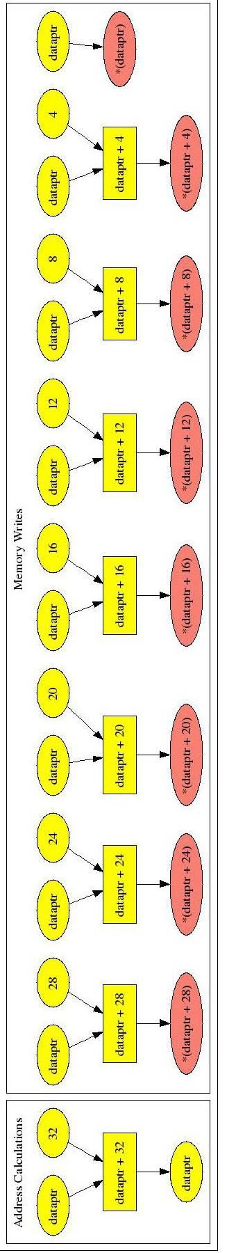
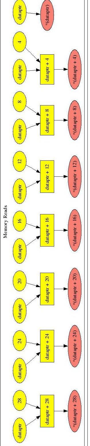
88 76
Institutionen för systemteknik
 Institutionen för systemteknik Department of Electrical Engineering Examensarbete Design and Implementation of a DMA Controller for Digital Signal Processor Examensarbete utfört i Datorteknik vid Tekniska
FLYNN S TAXONOMY OF COMPUTER ARCHITECTURE
 FLYNN S TAXONOMY OF COMPUTER ARCHITECTURE The most popular taxonomy of computer architecture was defined by Flynn in 1966. Flynn s classification scheme is based on the notion of a stream of information.
Linköping University Post Print. epuma: a novel embedded parallel DSP platform for predictable computing
 Linköping University Post Print epuma: a novel embedded parallel DSP platform for predictable computing Jian Wang, Joar Sohl, Olof Kraigher and Dake Liu N.B.: When citing this work, cite the original article.
Embedded processors. Timo Töyry Department of Computer Science and Engineering Aalto University, School of Science timo.toyry(at)aalto.
aalto.") Embedded processors Timo Töyry Department of Computer Science and Engineering Aalto University, School of Science timo.toyry(at)aalto.fi Comparing processors Evaluating processors Taxonomy of processors
Embedded processors Timo Töyry Department of Computer Science and Engineering Aalto University, School of Science timo.toyry(at)aalto.fi Comparing processors Evaluating processors Taxonomy of processors
Design of a System-on-Chip Switched Network and its Design Support Λ
 Design of a System-on-Chip Switched Network and its Design Support Λ Daniel Wiklund y, Dake Liu Dept. of Electrical Engineering Linköping University S-581 83 Linköping, Sweden Abstract As the degree of
Introduction to Parallel Processing
 Babylon University College of Information Technology Software Department Introduction to Parallel Processing By Single processor supercomputers have achieved great speeds and have been pushing hardware
Institutionen för systemteknik
 Institutionen för systemteknik Department of Electrical Engineering Examensarbete Bus System for Coresonic SIMT DSP Examensarbete utfört i Elektroteknik vid Tekniska högskolan vid Linköpings universitet
Chapter 18 Parallel Processing
 Chapter 18 Parallel Processing Multiple Processor Organization Single instruction, single data stream - SISD Single instruction, multiple data stream - SIMD Multiple instruction, single data stream - MISD
Lecture 8: RISC & Parallel Computers. Parallel computers
 Lecture 8: RISC & Parallel Computers RISC vs CISC computers Parallel computers Final remarks Zebo Peng, IDA, LiTH 1 Introduction Reduced Instruction Set Computer (RISC) is an important innovation in computer
Computer and Hardware Architecture I. Benny Thörnberg Associate Professor in Electronics
 Computer and Hardware Architecture I Benny Thörnberg Associate Professor in Electronics Hardware architecture Computer architecture The functionality of a modern computer is so complex that no human can
PGT - A path generation toolbox for Matlab (v0.1)
") PGT - A path generation toolbox for Matlab (v0.1) Maria Nyström, Mikael Norrlöf Division of Automatic Control Department of Electrical Engineering Linköpings universitet, SE-581 83 Linköping, Sweden WWW:
PGT - A path generation toolbox for Matlab (v0.1) Maria Nyström, Mikael Norrlöf Division of Automatic Control Department of Electrical Engineering Linköpings universitet, SE-581 83 Linköping, Sweden WWW:
Terrain Rendering using Multiple Optimally Adapting Meshes (MOAM)
") Examensarbete LITH-ITN-MT-EX--04/018--SE Terrain Rendering using Multiple Optimally Adapting Meshes (MOAM) Mårten Larsson 2004-02-23 Department of Science and Technology Linköpings Universitet SE-601 74
Examensarbete LITH-ITN-MT-EX--04/018--SE Terrain Rendering using Multiple Optimally Adapting Meshes (MOAM) Mårten Larsson 2004-02-23 Department of Science and Technology Linköpings Universitet SE-601 74
Unit 9 : Fundamentals of Parallel Processing
 Unit 9 : Fundamentals of Parallel Processing Lesson 1 : Types of Parallel Processing 1.1. Learning Objectives On completion of this lesson you will be able to : classify different types of parallel processing
CMPE 511 TERM PAPER. Distributed Shared Memory Architecture. Seda Demirağ
 CMPE 511 TERM PAPER Distributed Shared Memory Architecture by Seda Demirağ 2005701688 1. INTRODUCTION: Despite the advances in processor design, users still demand more and more performance. Eventually,
Serial. Parallel. CIT 668: System Architecture 2/14/2011. Topics. Serial and Parallel Computation. Parallel Computing
 CIT 668: System Architecture Parallel Computing Topics 1. What is Parallel Computing? 2. Why use Parallel Computing? 3. Types of Parallelism 4. Amdahl s Law 5. Flynn s Taxonomy of Parallel Computers 6.
Processor Architecture and Interconnect
 Processor Architecture and Interconnect What is Parallelism? Parallel processing is a term used to denote simultaneous computation in CPU for the purpose of measuring its computation speeds. Parallel Processing
Institutionen för datavetenskap Department of Computer and Information Science
 Institutionen för datavetenskap Department of Computer and Information Science Final thesis Load management for a telecom charging system by Johan Bjerre LIU-IDA/LITH-EX-A--08/043--SE 2008-10-13 1 Linköpings
Computer and Information Sciences College / Computer Science Department CS 207 D. Computer Architecture. Lecture 9: Multiprocessors
 Computer and Information Sciences College / Computer Science Department CS 207 D Computer Architecture Lecture 9: Multiprocessors Challenges of Parallel Processing First challenge is % of program inherently
Written Exam / Tentamen
 Written Exam / Tentamen Computer Organization and Components / Datorteknik och komponenter (IS1500), 9 hp Computer Hardware Engineering / Datorteknik, grundkurs (IS1200), 7.5 hp KTH Royal Institute of
Computer organization by G. Naveen kumar, Asst Prof, C.S.E Department 1
 Pipelining and Vector Processing Parallel Processing: The term parallel processing indicates that the system is able to perform several operations in a single time. Now we will elaborate the scenario,
Design of CPU Simulation Software for ARMv7 Instruction Set Architecture
 Design of CPU Simulation Software for ARMv7 Instruction Set Architecture Author: Dillon Tellier Advisor: Dr. Christopher Lupo Date: June 2014 1 INTRODUCTION Simulations have long been a part of the engineering
Real Processors. Lecture for CPSC 5155 Edward Bosworth, Ph.D. Computer Science Department Columbus State University
 Real Processors Lecture for CPSC 5155 Edward Bosworth, Ph.D. Computer Science Department Columbus State University Instruction-Level Parallelism (ILP) Pipelining: executing multiple instructions in parallel
Advanced Parallel Architecture. Annalisa Massini /2017
 Advanced Parallel Architecture Annalisa Massini - 2016/2017 References Advanced Computer Architecture and Parallel Processing H. El-Rewini, M. Abd-El-Barr, John Wiley and Sons, 2005 Parallel computing
RISC Processors and Parallel Processing. Section and 3.3.6
 RISC Processors and Parallel Processing Section 3.3.5 and 3.3.6 The Control Unit When a program is being executed it is actually the CPU receiving and executing a sequence of machine code instructions.
ARM ARCHITECTURE. Contents at a glance:
 UNIT-III ARM ARCHITECTURE Contents at a glance: RISC Design Philosophy ARM Design Philosophy Registers Current Program Status Register(CPSR) Instruction Pipeline Interrupts and Vector Table Architecture
Introduction to parallel computing
 Introduction to parallel computing 2. Parallel Hardware Zhiao Shi (modifications by Will French) Advanced Computing Center for Education & Research Vanderbilt University Motherboard Processor https://sites.google.com/
Ten Reasons to Optimize a Processor
 By Neil Robinson SoC designs today require application-specific logic that meets exacting design requirements, yet is flexible enough to adjust to evolving industry standards. Optimizing your processor
Institutionen för systemteknik
 Institutionen för systemteknik Department of Electrical Engineering Examensarbete Investigation of NoGap - SIMD Datapath Implementation Examensarbete utfört i Reglerteknik vid Tekniska högskolan vid Linköpings
Moore s Law. Computer architect goal Software developer assumption
 Moore s Law The number of transistors that can be placed inexpensively on an integrated circuit will double approximately every 18 months. Self-fulfilling prophecy Computer architect goal Software developer
Fundamentals of Computer Design
 Fundamentals of Computer Design Computer Architecture J. Daniel García Sánchez (coordinator) David Expósito Singh Francisco Javier García Blas ARCOS Group Computer Science and Engineering Department University
Lecture 9: MIMD Architectures
 Lecture 9: MIMD Architectures Introduction and classification Symmetric multiprocessors NUMA architecture Clusters Zebo Peng, IDA, LiTH 1 Introduction A set of general purpose processors is connected together.
Lecture 7: Parallel Processing
 Lecture 7: Parallel Processing Introduction and motivation Architecture classification Performance evaluation Interconnection network Zebo Peng, IDA, LiTH 1 Performance Improvement Reduction of instruction
ECE902 Virtual Machine Final Project: MIPS to CRAY-2 Binary Translation
 ECE902 Virtual Machine Final Project: MIPS to CRAY-2 Binary Translation Weiping Liao, Saengrawee (Anne) Pratoomtong, and Chuan Zhang Abstract Binary translation is an important component for translating
Architectures of Flynn s taxonomy -- A Comparison of Methods
 Architectures of Flynn s taxonomy -- A Comparison of Methods Neha K. Shinde Student, Department of Electronic Engineering, J D College of Engineering and Management, RTM Nagpur University, Maharashtra,
Multiprocessors & Thread Level Parallelism
 Multiprocessors & Thread Level Parallelism COE 403 Computer Architecture Prof. Muhamed Mudawar Computer Engineering Department King Fahd University of Petroleum and Minerals Presentation Outline Introduction
Synthesis-driven Derivation of Process Graphs from Functional Blocks for Time-Triggered Embedded Systems. Ghennadii Sivatki
 Master Thesis Synthesis-driven Derivation of Process Graphs from Functional Blocks for Time-Triggered Embedded Systems by Ghennadii Sivatki LITH-IDA/DS-EX--05/010--SE 2005-11-25 Avdelning, institution
Pipelining and Vector Processing
 Chapter 8 Pipelining and Vector Processing 8 1 If the pipeline stages are heterogeneous, the slowest stage determines the flow rate of the entire pipeline. This leads to other stages idling. 8 2 Pipeline
MULTIPROCESSORS AND THREAD-LEVEL. B649 Parallel Architectures and Programming
 MULTIPROCESSORS AND THREAD-LEVEL PARALLELISM B649 Parallel Architectures and Programming Motivation behind Multiprocessors Limitations of ILP (as already discussed) Growing interest in servers and server-performance
Parallel Computing: Parallel Architectures Jin, Hai
 Parallel Computing: Parallel Architectures Jin, Hai School of Computer Science and Technology Huazhong University of Science and Technology Peripherals Computer Central Processing Unit Main Memory Computer
Institutionen för systemteknik
 Institutionen för systemteknik Department of Electrical Engineering Examensarbete Machine Learning for detection of barcodes and OCR Examensarbete utfört i Datorseende vid Tekniska högskolan vid Linköpings
Institutionen för systemteknik
 Institutionen för systemteknik Department of Electrical Engineering Examensarbete Baseband Processing Using the Julia Language Examensarbete utfört i Elektroteknik vid Tekniska högskolan vid Linköpings
Computer parallelism Flynn s categories
 04 Multi-processors 04.01-04.02 Taxonomy and communication Parallelism Taxonomy Communication alessandro bogliolo isti information science and technology institute 1/9 Computer parallelism Flynn s categories
Lecture 9: MIMD Architectures
 Lecture 9: MIMD Architectures Introduction and classification Symmetric multiprocessors NUMA architecture Clusters Zebo Peng, IDA, LiTH 1 Introduction MIMD: a set of general purpose processors is connected
CS 426 Parallel Computing. Parallel Computing Platforms
 CS 426 Parallel Computing Parallel Computing Platforms Ozcan Ozturk http://www.cs.bilkent.edu.tr/~ozturk/cs426/ Slides are adapted from ``Introduction to Parallel Computing'' Topic Overview Implicit Parallelism:
MULTIPROCESSORS AND THREAD-LEVEL PARALLELISM. B649 Parallel Architectures and Programming
 MULTIPROCESSORS AND THREAD-LEVEL PARALLELISM B649 Parallel Architectures and Programming Motivation behind Multiprocessors Limitations of ILP (as already discussed) Growing interest in servers and server-performance
Computer Organization. Chapter 16
 William Stallings Computer Organization and Architecture t Chapter 16 Parallel Processing Multiple Processor Organization Single instruction, single data stream - SISD Single instruction, multiple data
Part IV. Chapter 15 - Introduction to MIMD Architectures
 D. Sima, T. J. Fountain, P. Kacsuk dvanced Computer rchitectures Part IV. Chapter 15 - Introduction to MIMD rchitectures Thread and process-level parallel architectures are typically realised by MIMD (Multiple
Introduction to Multiprocessors (Part I) Prof. Cristina Silvano Politecnico di Milano
 Prof. Cristina Silvano Politecnico di Milano") Introduction to Multiprocessors (Part I) Prof. Cristina Silvano Politecnico di Milano Outline Key issues to design multiprocessors Interconnection network Centralized shared-memory architectures Distributed
Introduction to Multiprocessors (Part I) Prof. Cristina Silvano Politecnico di Milano Outline Key issues to design multiprocessors Interconnection network Centralized shared-memory architectures Distributed
Data Parallel Architectures
 EE392C: Advanced Topics in Computer Architecture Lecture #2 Chip Multiprocessors and Polymorphic Processors Thursday, April 3 rd, 2003 Data Parallel Architectures Lecture #2: Thursday, April 3 rd, 2003
CMSC 611: Advanced. Parallel Systems
 CMSC 611: Advanced Computer Architecture Parallel Systems Parallel Computers Definition: A parallel computer is a collection of processing elements that cooperate and communicate to solve large problems
CS 352H Computer Systems Architecture Exam #1 - Prof. Keckler October 11, 2007
 CS 352H Computer Systems Architecture Exam #1 - Prof. Keckler October 11, 2007 Name: Solutions (please print) 1-3. 11 points 4. 7 points 5. 7 points 6. 20 points 7. 30 points 8. 25 points Total (105 pts):
Institutionen för systemteknik
 Institutionen för systemteknik Department of Electrical Engineering Examensarbete Implementations of the FFT algorithm on GPU Examensarbete utfört i Elektroniksystem vid Tekniska högskolan vid Linköpings
Fundamentals of Computers Design
 Computer Architecture J. Daniel Garcia Computer Architecture Group. Universidad Carlos III de Madrid Last update: September 8, 2014 Computer Architecture ARCOS Group. 1/45 Introduction 1 Introduction 2
UNIT I (Two Marks Questions & Answers)
") UNIT I (Two Marks Questions & Answers) Discuss the different ways how instruction set architecture can be classified? Stack Architecture,Accumulator Architecture, Register-Memory Architecture,Register-
UNIT I (Two Marks Questions & Answers) Discuss the different ways how instruction set architecture can be classified? Stack Architecture,Accumulator Architecture, Register-Memory Architecture,Register-
Parallel Processors. Session 1 Introduction
 Parallel Processors Session 1 Introduction Applications of Parallel Processors Structural Analysis Weather Forecasting Petroleum Exploration Fusion Energy Research Medical Diagnosis Aerodynamics Simulations
Architectural Support for Reducing Parallel Processing Overhead in an Embedded Multiprocessor
 2010 IEEE/IFIP International Conference on Embedded and Ubiquitous Computing Architectural Support for Reducing Parallel Processing Overhead in an Embedded Multiprocessor Jian Wang, Joar Sohl and Dake
Top500 Supercomputer list
 Top500 Supercomputer list Tends to represent parallel computers, so distributed systems such as SETI@Home are neglected. Does not consider storage or I/O issues Both custom designed machines and commodity
Lecture 9: MIMD Architecture
 Lecture 9: MIMD Architecture Introduction and classification Symmetric multiprocessors NUMA architecture Cluster machines Zebo Peng, IDA, LiTH 1 Introduction MIMD: a set of general purpose processors is
Von Neumann architecture. The first computers used a single fixed program (like a numeric calculator).
.") Microprocessors Von Neumann architecture The first computers used a single fixed program (like a numeric calculator). To change the program, one has to re-wire, re-structure, or re-design the computer.
Microprocessors Von Neumann architecture The first computers used a single fixed program (like a numeric calculator). To change the program, one has to re-wire, re-structure, or re-design the computer.
04 - DSP Architecture and Microarchitecture
 September 11, 2015 Memory indirect addressing (continued from last lecture) ; Reality check: Data hazards! ; Assembler code v3: repeat 256,endloop load r0,dm1[dm0[ptr0++]] store DM0[ptr1++],r0 endloop:
Module 5 Introduction to Parallel Processing Systems
 Module 5 Introduction to Parallel Processing Systems 1. What is the difference between pipelining and parallelism? In general, parallelism is simply multiple operations being done at the same time.this
Introduction. CSCI 4850/5850 High-Performance Computing Spring 2018
 Introduction CSCI 4850/5850 High-Performance Computing Spring 2018 Tae-Hyuk (Ted) Ahn Department of Computer Science Program of Bioinformatics and Computational Biology Saint Louis University What is Parallel
Embedded Systems Dr. Santanu Chaudhury Department of Electrical Engineering Indian Institution of Technology, Delhi
 Embedded Systems Dr. Santanu Chaudhury Department of Electrical Engineering Indian Institution of Technology, Delhi Lecture - 34 Compilers for Embedded Systems Today, we shall look at the compilers, which
Parallel Processing. Computer Architecture. Computer Architecture. Outline. Multiple Processor Organization
 Computer Architecture Computer Architecture Prof. Dr. Nizamettin AYDIN naydin@yildiz.edu.tr nizamettinaydin@gmail.com Parallel Processing http://www.yildiz.edu.tr/~naydin 1 2 Outline Multiple Processor
Computer Architecture
 Computer Architecture Slide Sets WS 2013/2014 Prof. Dr. Uwe Brinkschulte M.Sc. Benjamin Betting Part 3 Fundamentals in Computer Architecture Computer Architecture Part 3 page 1 of 55 Prof. Dr. Uwe Brinkschulte,
Motivation for Parallelism. Motivation for Parallelism. ILP Example: Loop Unrolling. Types of Parallelism
 Motivation for Parallelism Motivation for Parallelism The speed of an application is determined by more than just processor speed. speed Disk speed Network speed... Multiprocessors typically improve the
Institutionen för systemteknik
 Institutionen för systemteknik Department of Electrical Engineering Examensarbete Low Cost Floating-Point Extensions to a Fixed-Point SIMD Datapath Examensarbete utfört i Datorteknik vid Tekniska högskolan
EITF20: Computer Architecture Part4.1.1: Cache - 2
 EITF20: Computer Architecture Part4.1.1: Cache - 2 Liang Liu liang.liu@eit.lth.se 1 Outline Reiteration Cache performance optimization Bandwidth increase Reduce hit time Reduce miss penalty Reduce miss
The ARCUS Planning Framework for UAV Surveillance with EO/IR Sensors
 Technical report from Automatic Control at Linköpings universitet The ARCUS Planning Framework for UAV Surveillance with EO/IR Sensors Per Skoglar Division of Automatic Control E-mail: skoglar@isy.liu.se
Computer Caches. Lab 1. Caching
 Lab 1 Computer Caches Lab Objective: Caches play an important role in computational performance. Computers store memory in various caches, each with its advantages and drawbacks. We discuss the three main
CS 475: Parallel Programming Introduction
 CS 475: Parallel Programming Introduction Wim Bohm, Sanjay Rajopadhye Colorado State University Fall 2014 Course Organization n Let s make a tour of the course website. n Main pages Home, front page. Syllabus.
CS4961 Parallel Programming. Lecture 3: Introduction to Parallel Architectures 8/30/11. Administrative UPDATE. Mary Hall August 30, 2011
 CS4961 Parallel Programming Lecture 3: Introduction to Parallel Architectures Administrative UPDATE Nikhil office hours: - Monday, 2-3 PM, MEB 3115 Desk #12 - Lab hours on Tuesday afternoons during programming
ENGN1640: Design of Computing Systems Topic 06: Advanced Processor Design
 ENGN1640: Design of Computing Systems Topic 06: Advanced Processor Design Professor Sherief Reda http://scale.engin.brown.edu Electrical Sciences and Computer Engineering School of Engineering Brown University
POWERVR MBX. Technology Overview
 POWERVR MBX Technology Overview Copyright 2009, Imagination Technologies Ltd. All Rights Reserved. This publication contains proprietary information which is subject to change without notice and is supplied
BlueGene/L (No. 4 in the Latest Top500 List)
") BlueGene/L (No. 4 in the Latest Top500 List) first supercomputer in the Blue Gene project architecture. Individual PowerPC 440 processors at 700Mhz Two processors reside in a single chip. Two chips reside
BlueGene/L (No. 4 in the Latest Top500 List) first supercomputer in the Blue Gene project architecture. Individual PowerPC 440 processors at 700Mhz Two processors reside in a single chip. Two chips reside
Fundamental Concepts of Parallel Programming
 Fundamental Concepts of Parallel Programming Abstract The concepts behind programming methodologies and techniques are always under development, becoming more complex and flexible to meet changing computing
An Instruction Stream Compression Technique 1
 An Instruction Stream Compression Technique 1 Peter L. Bird Trevor N. Mudge EECS Department University of Michigan {pbird,tnm}@eecs.umich.edu Abstract The performance of instruction memory is a critical
Flit Synchronous Aelite Network on Chip. Mahesh Balaji Subburaman
 Flit Synchronous Aelite Network on Chip Examensarbete utfört i Elektroniksystem vid Tekniska högskolan i Linköping av Mahesh Balaji Subburaman LiTH - ISY - EX -- 08 / 4198 -- SE Linköping 2008 Flit Synchronous
Cray XE6 Performance Workshop
 Cray XE6 erformance Workshop odern HC Architectures David Henty d.henty@epcc.ed.ac.uk ECC, University of Edinburgh Overview Components History Flynn s Taxonomy SID ID Classification via emory Distributed
Computer and Hardware Architecture II. Benny Thörnberg Associate Professor in Electronics
 Computer and Hardware Architecture II Benny Thörnberg Associate Professor in Electronics Parallelism Microscopic vs Macroscopic Microscopic parallelism hardware solutions inside system components providing
Moore s Law. Computer architect goal Software developer assumption
 Moore s Law The number of transistors that can be placed inexpensively on an integrated circuit will double approximately every 18 months. Self-fulfilling prophecy Computer architect goal Software developer
Design of Embedded DSP Processors
 Design of Embedded DSP Processors Unit 3: Microarchitecture, Register file, and ALU 9/11/2017 Unit 3 of TSEA26-2017 H1 1 Contents 1. Microarchitecture and its design 2. Hardware design fundamentals 3.
COMPILER CONSTRUCTION FOR A NETWORK IDENTIFICATION SUMIT SONI PRAVESH KUMAR
 COMPILER CONSTRUCTION FOR A NETWORK IDENTIFICATION SUMIT SONI 13 PRAVESH KUMAR language) into another computer language (the target language, often having a binary form known as object code The most common
Parallel Architectures
 Parallel Architectures CPS343 Parallel and High Performance Computing Spring 2018 CPS343 (Parallel and HPC) Parallel Architectures Spring 2018 1 / 36 Outline 1 Parallel Computer Classification Flynn s
ARM Processors for Embedded Applications
 ARM Processors for Embedded Applications Roadmap for ARM Processors ARM Architecture Basics ARM Families AMBA Architecture 1 Current ARM Core Families ARM7: Hard cores and Soft cores Cache with MPU or
Ti Parallel Computing PIPELINING. Michał Roziecki, Tomáš Cipr
 Ti5317000 Parallel Computing PIPELINING Michał Roziecki, Tomáš Cipr 2005-2006 Introduction to pipelining What is this What is pipelining? Pipelining is an implementation technique in which multiple instructions
LECTURE 4: LARGE AND FAST: EXPLOITING MEMORY HIERARCHY
 LECTURE 4: LARGE AND FAST: EXPLOITING MEMORY HIERARCHY Abridged version of Patterson & Hennessy (2013):Ch.5 Principle of Locality Programs access a small proportion of their address space at any time Temporal
Computer Organization and Design, 5th Edition: The Hardware/Software Interface
 Computer Organization and Design, 5th Edition: The Hardware/Software Interface 1 Computer Abstractions and Technology 1.1 Introduction 1.2 Eight Great Ideas in Computer Architecture 1.3 Below Your Program
Institutionen för systemteknik
 Institutionen för systemteknik Department of Electrical Engineering Examensarbete Automated Fault Tree Generation from Requirement Structures Examensarbete utfört i Fordonssystem vid Tekniska högskolan
UG4 Honours project selection: Talk to Vijay or Boris if interested in computer architecture projects
 Announcements UG4 Honours project selection: Talk to Vijay or Boris if interested in computer architecture projects Inf3 Computer Architecture - 2017-2018 1 Last time: Tomasulo s Algorithm Inf3 Computer
CSCI 4717 Computer Architecture
 CSCI 4717/5717 Computer Architecture Topic: Symmetric Multiprocessors & Clusters Reading: Stallings, Sections 18.1 through 18.4 Classifications of Parallel Processing M. Flynn classified types of parallel
Chap. 4 Multiprocessors and Thread-Level Parallelism
 Chap. 4 Multiprocessors and Thread-Level Parallelism Uniprocessor performance Performance (vs. VAX-11/780) 10000 1000 100 10 From Hennessy and Patterson, Computer Architecture: A Quantitative Approach,
Institutionen för systemteknik
 Institutionen för systemteknik Department of Electrical Engineering Examensarbete Image interpolation in firmware for 3D display Examensarbete utfört i Elektroniksystem vid Tekniska högskolan i Linköping
Structural Algorithms for Diagnostic System Design Using Simulink Models
 Structural Algorithms for Diagnostic System Design Using Simulink Models Master s thesis performed in Vehicular Systems by Lars Eriksson Reg nr: LiTH-ISY-EX-3601-2004 10th January 2005 Structural Algorithms
Tutorial 11. Final Exam Review
 Tutorial 11 Final Exam Review Introduction Instruction Set Architecture: contract between programmer and designers (e.g.: IA-32, IA-64, X86-64) Computer organization: describe the functional units, cache
Institutionen för systemteknik
 Institutionen för systemteknik Department of Electrical Engineering Examensarbete Real-Time Multi-Dimensional Fast Fourier Transforms on FPGAs Examensarbete utfört i Datorteknik vid Tekniska högskolan
The Nios II Family of Configurable Soft-core Processors
 The Nios II Family of Configurable Soft-core Processors James Ball August 16, 2005 2005 Altera Corporation Agenda Nios II Introduction Configuring your CPU FPGA vs. ASIC CPU Design Instruction Set Architecture
Optimising for the p690 memory system
 Optimising for the p690 memory Introduction As with all performance optimisation it is important to understand what is limiting the performance of a code. The Power4 is a very powerful micro-processor
Computing on GPUs. Prof. Dr. Uli Göhner. DYNAmore GmbH. Stuttgart, Germany
 Computing on GPUs Prof. Dr. Uli Göhner DYNAmore GmbH Stuttgart, Germany Summary: The increasing power of GPUs has led to the intent to transfer computing load from CPUs to GPUs. A first example has been
Control Hazards. Branch Prediction
 Control Hazards The nub of the problem: In what pipeline stage does the processor fetch the next instruction? If that instruction is a conditional branch, when does the processor know whether the conditional