VHDL Implementation of Arithmetic Logic Unit
|
|
|
- Jonah Ford
- 5 years ago
- Views:
Transcription
1 VHDL Implementation of Arithmetic Logic Unit 1 Saumyakanta Sarangi Associate Professor Electronics & Telecommunication Engg Eastern Academy of Science & Technology Bhubaneswar, India 2 Sangita Swain Associate Professor Electronics & Telecommunication Engg Eastern Academy of Science & Technology Bhubaneswar, India 3 Swagatika Dash Assistant Professor Electronics & Telecommunication Engg Eastern Academy of Science & Technology Bhubaneswar, India 4 Manas Ranjan Mohanta Assistant Professor Electronics & Telecommunication Engg Eastern Academy of Science & Technology Bhubaneswar, India Abstract Digital design is an amazing and very broad field. The applications of digital design are present in our daily life, including computers, calculators, video cameras etc. The VHDL (VHSIC Hardware Description Language) has become an essential tool for designers in the world of digital design. This paper presents implementation of a 4- bit Arithmetic Logic Unit (ALU) using VHDL. ALU of digital computers is an aspect of logic design with the objective of developing appropriate algorithms in order to achieve an efficient utilization of the available hardware. Here the mixed VHDL model of ALU is designed to perform 11 operations which includes both logical and arithmetic operations. The VHDL implementation and functionality test of the 4-bit ALU is done by using the Xilinx ISE 9.2i tool. Keywords ALU, VHDL, XILINX I. INTRODUCTION An arithmetic logic unit (ALU) is a multi operation, combinational-logic digital function. It can perform a set of basic arithmetic operations and a set of logic operations. The ALU has a number of selection lines to select a particular operation in the unit. The selection lines are decoded within the ALU so that K selection variables can specify up to 2^k distinct operations. Figure:1. (Block diagram of a 4-bit ALU ) Figure 1 shows the block diagram of a 4-bit ALU. The four data inputs from A are combined with the four inputs from B to generate an operation at the F outputs. The mode-select input s2 distinguishes between arithmetic and logic operations. The two function-select input s1 and s0 specify the particular arithmetic or logic operation to be generated. With three selection variables, it is possible to specify four arithmetic operations (with s2 in one state) and four logic operations (with s2 in the other state). The input and output carries have meaning only during an arithmetic operation. The input carry in the least significant position of an ALU is quite often used as a fourth selection variable that can double the number of arithmetic operations. In this way, it is possible to generate four more operations, for a total of eight arithmetic operations. The design of a typical ALU will be carried out in three stages. First, the design of arithmetic section will be undertaken. Second, the design of logic section will be considered. Finally, the arithmetic section will be modified so that it can perform both arithmetic and logic operations. II. DESIGN OF ALU We design an ALU with seven arithmetic operations and four logic operations. Three selection variables s2, s1, and s0 select eight different operations, and the input carry Cin is used to select four additional arithmetic operations. With s2=0, selection variables s1 and s0 together with Cin will select eight arithmetic operations in arithmetic table above. With s2 = 1 variables s1 and s0 will select the four logic operations OR, XOR, AND, and NOT. The design of an ALU is a combinational logic. Because the unit has a regular pattern, it can be broken into identical stages connected in cascade through the carries. We can design one stage of ALU and then duplicate it for the number of stages required. There are six inputs to each stage: Ai, Bi, Ci, s2, s1, and s0. There are two outputs in each stage: output Fi and the carry out Ci+1. One can formulate a truth table with 64 entries and simplify the two output function.here we choose to employ an alternative procedure that uses the 1214
2 availability of a parallel adder. The steps involved in the design of an ALU are as follows: Design the arithmetic section independent of the logic section.determine the logic operations obtained from the arithmetic circuit in step 1, assuming that the input carries to all stages are 0.Modify the arithmetic circuit to obtain the required logic operations. The final ALU is shown below. The inputs to each full-adder circuit are specified by the Boolean function: Xi = Ai + s2.s1. s0. Bi + s2.s1.s0.bi Yi = s0.bi + s1.bi Zi = s2.ci When s2 = 0, three functions reduce to: Xi = Ai Yi = s0.bi + s1.bi Zi = Ci Which are the functions for the arithmetic circuit of above figure. The logic operations are generated when s2 = 1. For s2s1s0 = 101 or 111, the functions reduce to: Xi = Ai Yi = s0.bi + s1.bi Ci = 0 Output Fi is then equal to Xi (+) Yi and produces the exclusive-or and complement operations as specified in above table. When s2s1s0 = 110, each Ai is ORed with Bi to provide the AND operation as explained previously. The 12 operations generated in the ALU are summarized in below truth table. The particular function is selected through s2, s1, s0, and Cin. The arithmetic operations are identical to the ones listed for the arithmetic circuit. The value of Cin for the four logic functions has no effect on the operation of the unit and those entries are marked with don t-care X s. Table:1 [ FUNCTION TABLE OF ALU ] Selection Output Function s2 s1 s0 cin F = A Transfer A F = A+1 Increment A F = A+B Addition F= A+B+1 Add with carry F = A-B-1 Subtract with borrow F= A-B Subtraction F = A-1 Decrement A F = A Transfer A x F = A V B OR x F = AΘ B XOR x F = A Ʌ B AND x F = A Complement A Figure:2 [ LOGIC DIAGRAM OF ARITHMETIC LOGIC ] Design of Arithmetic Unit UNIT (ALU) The basic component of the arithmetic section of an ALU is a parallel adder. A parallel adder is constructed with a number of a full-adder circuits connected in cascade. By controlling the data inputs to the parallel adder, it is possible to obtain different types of arithmetic operations. Figure 3 demonstrates the arithmetic operations obtained when one set of inputs to a parallel adder is controlled externally. The number of bits in the parallel adder may be of any value. The input carry Cin goes to the full-adder circuit in the least significant bit position. The output carry Cout comes from the full-adder circuit in the most significant bit position. The arithmetic addition is achieved when one set of inputs receives a binary number A, the other set of inputs receives a binary number B, and the input carry is maintained at 0. This is shown in (a). By making Cin = 1 as in (b), it is possible to add 1 to the sum in F. Now let us consider the effect of complementing all the bits of input B. With Cin = 0, the output produces F = A + (comp B), which is the sum of A plus the 1 s complement of B. 1215
3 the output Yi = 0, regardless of the value of Bi. When s1s0 = 01, the top AND gate generates the value of Bi while the bottom gate output is 0; so Yi = Bi. With s1s0 = 10, the bottom AND gate generates the complement of Bi to give Yi = Bi`. When s1s0 = 11, both gates are active and Yi = Bi + Bi` = 1. S1 S0 Y Bi 1 0 Bi Figure:3 [ Parallel Adder Arithmetic Operations] Adding 1 to this sum by making Cin = 1, we obtain F = A+ (comp B) + 1, which produces the sum of A plus the 2 s complement of B. This operation is similar to a subtraction operation if the output carry is discarded. If we force all 0 s into the B terminals, we obtain F = A + 0 = A, which transfers input A into output F. Adding 1 through Cin as in (f), we obtain F = A + 1, which is the increment operation. The condition illustrated in (g) inserts all 1 s into the B terminals. This produces the decrement operation F = A 1. To show this condition is indeed a decrement operation, consider a parallel adder with n full-adder circuits. When the output carry is 1, it represents the number 2^n because 2^n in binary consists of a 1 followed n 0 s. Subtracting 1 from 2^n, we obtain 2^n 1, which in binary is a number of n 1 s. Adding 2^n 1 to A, we obtain F =A + 2^n + A 1. If the output carry 2^n is removed, we obtain F = A 1. A 4-bit arithmetic circuit that performs eight arithmetic operations is shown in figure below. The four full-adder (FA) circuits constitute the parallel adder. The carry into the first stage is the input carry.the carry out of the forth stage is the output carry. All other carries Are connected internally from one stage to the next. The selection variables are S1, S0 and Cin. Variables S1 and S0 control all of the B inputs to the fulladder circuits as in figure. The A inputs go directly to the other inputs of the full-adders. The circuit that controls input B to provide the functions i.e. true/complement, one/zero element. The circuit is illustrated in above diagram. The two selection lines s1 and s0 control the input of each B terminal. The diagram shows one typical input designated by Bi and an output designated by Yi. In typical application, there are n such circuits for i= 1, 2, 3.n. As shown in the table below, when both s1 and s0 are equal to 0, Figure:4.a [ Logic Diagram Of Arithmetic Circuit ] 1216
4 The arithmetic operations implemented in the arithmetic circuit are listed in below table 2. The values of the Y inputs to the full-adder circuits are a function of selection variables S1 and S0. selection variables in the multiplexer select one of the gates for the output. The table above shows output logic generated as a function of the two selection variables. Function select s2 s1 s0 Table:2 [ Function Table Of Arithmetic Unit ] Y Output Function F = A Transfer A F = A+1 Increment A B F = A+B Addition B F = A+B+1 Add with carry B F = A-B-1 Subtract with borrow B F= A-B Subtraction All 1 s F = A-1 Decrement A All 1 s F = A Transfer A Adding the value of Y in each case to the value of A plus the Cin value gives the arithmetic operation in each entry. The eight operations listed in the table follow directly from the function diagrams illustrated. This example demonstrates the feasibility of constructing an arithmetic circuit by means of a parallel adder. The combinational circuit that must be inserted in each stage between the external inputs Ai and Bi and the inputs of the parallel adder Xi and Yi is a function of the arithmetic operations that are to be implemented. The arithmetic circuit of fig needs a combinational circuit in each stage specified by the Boolean functions: Xi = Ai Yi = Bi S0 + Bi S1 i = 1,2,., n Where n is the number of bits in the arithmetic circuit. In each stage i, we use the same common selection variables S1 and S0. The combinational circuit will be different if the circuit generates different arithmetic operations. Figure:4.b [ Logic Diagram Of Logic Circuit ] The logic circuit can be combined with the arithmetic circuit to produce one arithmetic logic unit. Selection variables s1 and s0 can be made common to both sections provided we use a third selection variable, s2, to differentiate between the two. This configuration is shown below. The outputs of the logic and arithmetic circuits in each stage goes through a multiplexer with selection variable s2. When s2 = 0, the arithmetic output is selected, but when s2 = 1, the logic output is selected. A. Design of Logic Unit The logic micro operations manipulate the bits of the operands separately and treat each bit as a binary variable. There are 16 operations that can be performed with two binary variables. The 16 logic operations can be generated in one circuit and selected by means of four selection lines. Since all logic operations can be obtained by means of AND, OR, and NOT (complement) operations, it may be more convenient to employ a logic circuit with just these operations. For three operations, we need two selection variables. But two selection lines can select among four logic operations, so we choose also the exclusive-or (XOR) function for the logic circuit to be designed in this part. The diagram shown below shows a typical stage designated by subscript i. The four gates generate the four logic operations OR, XOR, AND, and NOT. The two Figure:4.c [ Combining logic and arithmetic circuit ] A more efficient ALU can be obtained if we investigate the possibility of generating logic operations in an already available arithmetic circuit. This can be done by inhibiting all input carries into the full-adder circuits of the parallel adder. Let we consider the Boolean function that generates the output sum in a full-adder circuit: Fi=Xi (+) Yi (+) Ci The input carry Ci in each stage can be made to be equal to 0 when a selection variable s2 is equal to 1. The result would be: Fi = Xi (+) Yi 1217


 III. RESULT It is needed to test whether the design works to meet the given specification to ensure that designed entity is correct.")

5 This expression is valid because of the property of the exclusive-or operation X (+) 0 = X. Thus, with the input carry to each stage equal to 0, the full-adder circuits generate the exclusive-or operation. Now consider the arithmetic circuit, the value of Yi can be selected by means of the two selection variables to be equal to either 0, Bi, Bi, or 1. The value of Xi is always equal to input Ai. The below table shows the four logic operations obtained when a third selection variable s2 = 1. This selection variable forces Ci to be equal to 0 while s1 and s0 choose a particular value for Yi. The four logic operations obtained by this configuration are transfer, exclusive-or, equivalence, and complement. The third entry is the equivalence operation because: Ai (+) Bi = AiBi + Ai Bi = Ai (.) Bi The last entry in the table is the NOT or complement operation because: Ai (+) 1 = Ai Figure:7. b (S2 S1 S0=000, Cin=1 :Increment A i.e. A + 1) III. RESULT It is needed to test whether the design works to meet the given specification to ensure that designed entity is correct. This is verified by the process of simulation. The process of simulation uses a test bench to test the design whether it behaves correctly by stimulating it with artificial input and monitoring the output. The simulation is carried out by using the Xilinx ISE 9.2i tool l and having the test bench and the behavioral design code for 4-bit ALU in the same project folder. We observed from the simulation results that the 4-bit ALU implemented by the above described method and code, worked successfully for all the input combinations and the select codes according to the given specification in Table 1. The simulation results and RTL Schematics are shown below in Fig.7 and Fig.8 respectively A. Simulation Results Figure:7. c (S2 S1 S0=001, Cin=0 : A + B) Figure:7. a (S2 S1 S0=000, Cin=0 : Transfer A) Figure:7. d (S2 S1 S0=001, Cin=1 : A + B+1) 1218


 f (S2 S1")
 i (S2 S1")
 g Cin=0 :")
 j (S2 S1")
 1219")
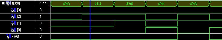
6 Figure:7. e (S2 S1 S0=010, Cin=0 : A B 1) Figure:7.h (S2 S1 S0=011, Cin=1 : Transfer A) Figure:7. f (S2 S1 S0=010, Cin=1 : A - B) Figure:7. i (S2 S1 S0=100, Cin=x : A OR B) Figure:7.g (S2 S1 S0=011, Cin=0 : Decrement A i.e. A 1) Figure:7. j (S2 S1 S0=101, Cin=x : A XOR B) 1219
 B. RTL SCEMATIC OF ALU: Figure:8. c Figure:8. d IV.")


7 Figure:7. k (S2 S1 S0=110, Cin=x : A AND B) Figure:8.b Figure:7. l (S2 S1 S0=111, Cin=x : Complement of A) B. RTL SCEMATIC OF ALU: Figure:8. c Figure:8. d IV. CONCLUSION & FUTURE WORKS This study helped to understand the complete flow of RTL design, starting from designing a top level RTL module for 4- bit ALU using hardware description language, VHDL. Verification of the designed RTL code using simulation techniques, synthesis of RTL code to obtain gate level net list using Xilinx ISE tool and Arithmetic Logic Unit was successfully designed and simulated using Xilinx ISE 9.2i package. The ALU model is designed in such a manner that the whole module can be used as component to design 8,16,32 bit ALU using structural model. Figure:8.a 1220
8 REFERENCES [1] D. Gajski and R. Khun, Introduction: New VLSI Tools, IEEE Computer, Vol. 16, No. 12, pp , Dec [2] Douglas L. Perry, VHDL, third edition, McGraw-Hill, pp.60-63, 238, July [3] S.Yalamanchali, Introductory VHDL: From simulation to synthesis, Prentice Hall, United States, [4] [5] B.Stephen Brown, V.Zvonko, Fundamentals of digital logic with VHDL Design 2nd Edition, Mc Graw Hill International Edition, [6] Charles H.Roth, Jr., Digital System Design using VHDL, PWS Publishing Company, [7] Mark Zwolinski, Digital System Design with VHDL, Prentice Hall, 2000.Pedroni, Digital Logic Design using VHDL. [8] S.Kaliamurthy, R.Muralidharan, VHDL Design of FPGA Arithmetic Processor International Conference on Engineering and ICT, [9] Xilinx Technologies, Xilinx Data Sheet for XC3S100E. direct. xilinx.com/bvdocs/ publications/ ds312.pdf. [10] [11] Prof. S. Kaliamurthy & Ms. U. Sowmmiya, VHDL design of arithmetic processor,global Journals Inc.(USA), November [12] Geetanjali and Nishant Tripathi VHDL Implementation of 32-Bit Arithmetic Logic Unit (Alu) [13] Shikha Khurana, Kanika Kaur Implementation of ALU using FPGA [14] Mr. Abhishek Gupta, Mr. Utsav Malviya, Prof. Vinod Kapse A Novel Approach to Design High Speed Arithmetic Logic Unit Based On Ancient Vedic Multiplication Technique International Journal of Modern Engineering Research (IJMER) Vol.2, Issue.4, July-Aug 2012 pp ISSN:
Prachi Sharma 1, Rama Laxmi 2, Arun Kumar Mishra 3 1 Student, 2,3 Assistant Professor, EC Department, Bhabha College of Engineering
 A Review: Design of 16 bit Arithmetic and Logical unit using Vivado 14.7 and Implementation on Basys 3 FPGA Board Prachi Sharma 1, Rama Laxmi 2, Arun Kumar Mishra 3 1 Student, 2,3 Assistant Professor,
Implementation of Low Power High Speed 32 bit ALU using FPGA
 Implementation of Low Power High Speed 32 bit ALU using FPGA J.P. Verma Assistant Professor (Department of Electronics & Communication Engineering) Maaz Arif; Brij Bhushan Choudhary& Nitish Kumar Electronics
UNIT-III REGISTER TRANSFER LANGUAGE AND DESIGN OF CONTROL UNIT
 UNIT-III 1 KNREDDY UNIT-III REGISTER TRANSFER LANGUAGE AND DESIGN OF CONTROL UNIT Register Transfer: Register Transfer Language Register Transfer Bus and Memory Transfers Arithmetic Micro operations Logic
Submitted by 1
 Submitted by WWW.ASSIGNMENTPOINT.COM 1 In computing, an Arithmetic Logic Unit (ALU) is a digital circuit that performs arithmetic and logical operations. The ALU is a fundamental building block of the
Design of 16 bit Arithmetic and Logical Unit Using Vivado 14.7 and Implementation on Basys 3 FPGA Board
 2016 IJSRSET Volume 2 Issue 5 Print ISSN: 2395-1990 Online ISSN : 2394-4099 Themed Section: Engineering and Technology Design of 16 bit Arithmetic and Logical Unit Using Vivado 14.7 and Implementation
32 bit Arithmetic Logical Unit (ALU) using VHDL
 using VHDL") 32 bit Arithmetic Logical Unit (ALU) using VHDL 1, Richa Singh Rathore 2 1 M. Tech Scholar, Department of ECE, Jayoti Vidyapeeth Women s University, Rajasthan, INDIA, dishamalik26@gmail.com 2 M. Tech Scholar,
32 bit Arithmetic Logical Unit (ALU) using VHDL 1, Richa Singh Rathore 2 1 M. Tech Scholar, Department of ECE, Jayoti Vidyapeeth Women s University, Rajasthan, INDIA, dishamalik26@gmail.com 2 M. Tech Scholar,
COMPUTER ARCHITECTURE AND ORGANIZATION Register Transfer and Micro-operations 1. Introduction A digital system is an interconnection of digital
 Register Transfer and Micro-operations 1. Introduction A digital system is an interconnection of digital hardware modules that accomplish a specific information-processing task. Digital systems vary in
Keywords: Soft Core Processor, Arithmetic and Logical Unit, Back End Implementation and Front End Implementation.
 ISSN 2319-8885 Vol.03,Issue.32 October-2014, Pages:6436-6440 www.ijsetr.com Design and Modeling of Arithmetic and Logical Unit with the Platform of VLSI N. AMRUTHA BINDU 1, M. SAILAJA 2 1 Dept of ECE,
REGISTER TRANSFER AND MICROOPERATIONS
 1 REGISTER TRANSFER AND MICROOPERATIONS Register Transfer Language Register Transfer Bus and Memory Transfers Arithmetic Microoperations Logic Microoperations Shift Microoperations Arithmetic Logic Shift
REGISTER TRANSFER LANGUAGE
 REGISTER TRANSFER LANGUAGE The operations executed on the data stored in the registers are called micro operations. Classifications of micro operations Register transfer micro operations Arithmetic micro
Register Transfer Language and Microoperations (Part 2)
") Register Transfer Language and Microoperations (Part 2) Adapted by Dr. Adel Ammar Computer Organization 1 MICROOPERATIONS Computer system microoperations are of four types: Register transfer microoperations
Register Transfer Language and Microoperations (Part 2) Adapted by Dr. Adel Ammar Computer Organization 1 MICROOPERATIONS Computer system microoperations are of four types: Register transfer microoperations
To design a 4-bit ALU To experimentally check the operation of the ALU
 1 Experiment # 11 Design and Implementation of a 4 - bit ALU Objectives: The objectives of this lab are: To design a 4-bit ALU To experimentally check the operation of the ALU Overview An Arithmetic Logic
DLD VIDYA SAGAR P. potharajuvidyasagar.wordpress.com. Vignana Bharathi Institute of Technology UNIT 3 DLD P VIDYA SAGAR
 DLD UNIT III Combinational Circuits (CC), Analysis procedure, Design Procedure, Combinational circuit for different code converters and other problems, Binary Adder- Subtractor, Decimal Adder, Binary Multiplier,
Designing an Improved 64 Bit Arithmetic and Logical Unit for Digital Signaling Processing Purposes
 Available Online at- http://isroj.net/index.php/issue/current-issue ISROJ Index Copernicus Value for 2015: 49.25 Volume 02 Issue 01, 2017 e-issn- 2455 8818 Designing an Improved 64 Bit Arithmetic and Logical
Combinational Logic with MSI and LSI
 1010101010101010101010101010101010101010101010101010101010101010101010101010101010 1010101010101010101010101010101010101010101010101010101010101010101010101010101010 1010101010101010101010101010101010101010101010101010101010101010101010101010101010
FPGA based Simulation of Clock Gated ALU Architecture with Multiplexed Logic Enable for Low Power Applications
 IJSRD - International Journal for Scientific Research & Development Vol. 3, Issue 04, 2015 ISSN (online): 2321-0613 FPGA based Simulation of Clock Gated ALU Architecture with Multiplexed Logic Enable for
Computer Organization (Autonomous)
") Computer Organization (Autonomous) UNIT I Sections - A & D Prepared by Anil Kumar Prathipati, Asst. Prof., Dept. of CSE. SYLLABUS Introduction: Types of Computers, Functional units of Basic Computer (Block
Computer Organization (Autonomous) UNIT I Sections - A & D Prepared by Anil Kumar Prathipati, Asst. Prof., Dept. of CSE. SYLLABUS Introduction: Types of Computers, Functional units of Basic Computer (Block
For Example: P: LOAD 5 R0. The command given here is used to load a data 5 to the register R0.
 Register Transfer Language Computers are the electronic devices which have several sets of digital hardware which are inter connected to exchange data. Digital hardware comprises of VLSI Chips which are
Arithmetic Circuits. Nurul Hazlina Adder 2. Multiplier 3. Arithmetic Logic Unit (ALU) 4. HDL for Arithmetic Circuit
 4. HDL for Arithmetic Circuit") Nurul Hazlina 1 1. Adder 2. Multiplier 3. Arithmetic Logic Unit (ALU) 4. HDL for Arithmetic Circuit Nurul Hazlina 2 Introduction 1. Digital circuits are frequently used for arithmetic operations 2. Fundamental
Nurul Hazlina 1 1. Adder 2. Multiplier 3. Arithmetic Logic Unit (ALU) 4. HDL for Arithmetic Circuit Nurul Hazlina 2 Introduction 1. Digital circuits are frequently used for arithmetic operations 2. Fundamental
EXPERIMENT #8: BINARY ARITHMETIC OPERATIONS
 EE 2 Lab Manual, EE Department, KFUPM EXPERIMENT #8: BINARY ARITHMETIC OPERATIONS OBJECTIVES: Design and implement a circuit that performs basic binary arithmetic operations such as addition, subtraction,
UNIT - V MEMORY P.VIDYA SAGAR ( ASSOCIATE PROFESSOR) Department of Electronics and Communication Engineering, VBIT
 Department of Electronics and Communication Engineering, VBIT") UNIT - V MEMORY P.VIDYA SAGAR ( ASSOCIATE PROFESSOR) contents Memory: Introduction, Random-Access memory, Memory decoding, ROM, Programmable Logic Array, Programmable Array Logic, Sequential programmable
UNIT - V MEMORY P.VIDYA SAGAR ( ASSOCIATE PROFESSOR) contents Memory: Introduction, Random-Access memory, Memory decoding, ROM, Programmable Logic Array, Programmable Array Logic, Sequential programmable
High speed Integrated Circuit Hardware Description Language), RTL (Register transfer level). Abstract:
, RTL (Register transfer level). Abstract:") based implementation of 8-bit ALU of a RISC processor using Booth algorithm written in VHDL language Paresh Kumar Pasayat, Manoranjan Pradhan, Bhupesh Kumar Pasayat Abstract: This paper explains the design
based implementation of 8-bit ALU of a RISC processor using Booth algorithm written in VHDL language Paresh Kumar Pasayat, Manoranjan Pradhan, Bhupesh Kumar Pasayat Abstract: This paper explains the design
VLSI Implementation of Adders for High Speed ALU
 VLSI Implementation of Adders for High Speed ALU Prashant Gurjar Rashmi Solanki Pooja Kansliwal Mahendra Vucha Asst. Prof., Dept. EC,, ABSTRACT This paper is primarily deals the construction of high speed
Chapter 4 Arithmetic Functions
 Logic and Computer Design Fundamentals Chapter 4 Arithmetic Functions Charles Kime & Thomas Kaminski 2008 Pearson Education, Inc. (Hyperlinks are active in View Show mode) Overview Iterative combinational
CHAPTER 4: Register Transfer Language and Microoperations
 CS 224: Computer Organization S.KHABET CHAPTER 4: Register Transfer Language and Microoperations Outline Register Transfer Language Register Transfer Bus and Memory Transfers Arithmetic Microoperations
COMBINATIONAL LOGIC CIRCUITS
 COMBINATIONAL LOGIC CIRCUITS 4.1 INTRODUCTION The digital system consists of two types of circuits, namely: (i) Combinational circuits and (ii) Sequential circuits A combinational circuit consists of logic
An FPGA based Implementation of Floating-point Multiplier
 An FPGA based Implementation of Floating-point Multiplier L. Rajesh, Prashant.V. Joshi and Dr.S.S. Manvi Abstract In this paper we describe the parameterization, implementation and evaluation of floating-point
EGC221: Digital Logic Lab
 EGC221: Digital Logic Lab Experiment #7 Arithmetic Logic Unit (ALU) Schematic Implementation Student s Name: Student s Name: Reg. no.: Reg. no.: Semester: Spring 2017 Date: 04 April 2017 Assessment: Assessment
An Efficient Design of Vedic Multiplier using New Encoding Scheme
 An Efficient Design of Vedic Multiplier using New Encoding Scheme Jai Skand Tripathi P.G Student, United College of Engineering & Research, India Priya Keerti Tripathi P.G Student, Jaypee University of
Implementation of Ripple Carry and Carry Skip Adders with Speed and Area Efficient
 ISSN (Online) : 2278-1021 Implementation of Ripple Carry and Carry Skip Adders with Speed and Area Efficient PUSHPALATHA CHOPPA 1, B.N. SRINIVASA RAO 2 PG Scholar (VLSI Design), Department of ECE, Avanthi
Chapter 3: part 3 Binary Subtraction
 Chapter 3: part 3 Binary Subtraction Iterative combinational circuits Binary adders Half and full adders Ripple carry and carry lookahead adders Binary subtraction Binary adder-subtractors Signed binary
REGISTER TRANSFER AND MICROOPERATIONS
 REGISTER TRANSFER AND MICROOPERATIONS Register Transfer Language Register Transfer Bus and Memory Transfers Arithmetic Microoperations Logic Microoperations Shift Microoperations Arithmetic Logic Shift
Combinational Logic II
 Combinational Logic II Ranga Rodrigo July 26, 2009 1 Binary Adder-Subtractor Digital computers perform variety of information processing tasks. Among the functions encountered are the various arithmetic
DESIGN AND IMPLEMENTATION OF VLSI SYSTOLIC ARRAY MULTIPLIER FOR DSP APPLICATIONS
 International Journal of Computing Academic Research (IJCAR) ISSN 2305-9184 Volume 2, Number 4 (August 2013), pp. 140-146 MEACSE Publications http://www.meacse.org/ijcar DESIGN AND IMPLEMENTATION OF VLSI
VLSI Based 16 Bit ALU with Interfacing Circuit
 Available online at www.ijiere.com International Journal of Innovative and Emerging Research in Engineering e-issn: 2394-3343 p-issn: 2394-5494 VLSI Based 16 Bit ALU with Interfacing Circuit Chandni N.
Register Transfer and Micro-operations
 Register Transfer Language Register Transfer Bus Memory Transfer Micro-operations Some Application of Logic Micro Operations Register Transfer and Micro-operations Learning Objectives After reading this
 Get Free notes at Module-I One s Complement: Complement all the bits.i.e. makes all 1s as 0s and all 0s as 1s Two s Complement: One s complement+1 SIGNED BINARY NUMBERS Positive integers (including zero)
Combinational and sequential circuits (learned in Chapters 1 and 2) can be used to create simple digital systems.
 can be used to create simple digital systems.") REGISTER TRANSFER AND MICROOPERATIONS Register Transfer Language Register Transfer Bus and Memory Transfers Arithmetic Microoperations Logic Microoperations Shift Microoperations Arithmetic Logic Shift
REGISTER TRANSFER AND MICROOPERATIONS Register Transfer Language Register Transfer Bus and Memory Transfers Arithmetic Microoperations Logic Microoperations Shift Microoperations Arithmetic Logic Shift
An Efficient Carry Select Adder with Less Delay and Reduced Area Application
 An Efficient Carry Select Adder with Less Delay and Reduced Area Application Pandu Ranga Rao #1 Priyanka Halle #2 # Associate Professor Department of ECE Sreyas Institute of Engineering and Technology,
Chapter 3 Part 2 Combinational Logic Design
 University of Wisconsin - Madison ECE/Comp Sci 352 Digital Systems Fundamentals Kewal K. Saluja and Yu Hen Hu Spring 2002 Chapter 3 Part 2 Combinational Logic Design Originals by: Charles R. Kime and Tom
Simulation Results Analysis Of Basic And Modified RBSD Adder Circuits 1 Sobina Gujral, 2 Robina Gujral Bagga
 Simulation Results Analysis Of Basic And Modified RBSD Adder Circuits 1 Sobina Gujral, 2 Robina Gujral Bagga 1 Assistant Professor Department of Electronics and Communication, Chandigarh University, India
The operations executed on data stored in registers(shift, clear, load, count)
") 4-4- Register Transfer Language Microoperation The operations executed on data stored in registers(shift, clear, load, count) Internal H/W Organization(best defined by specifying). The set of registers(register
4-4- Register Transfer Language Microoperation The operations executed on data stored in registers(shift, clear, load, count) Internal H/W Organization(best defined by specifying). The set of registers(register
DESIGN AND IMPLEMENTATION OF APPLICATION SPECIFIC 32-BITALU USING XILINX FPGA
 DESIGN AND IMPLEMENTATION OF APPLICATION SPECIFIC 32-BITALU USING XILINX FPGA T.MALLIKARJUNA 1 *,K.SREENIVASA RAO 2 1 PG Scholar, Annamacharya Institute of Technology & Sciences, Rajampet, A.P, India.
Chapter 6 Combinational-Circuit Building Blocks
 Chapter 6 Combinational-Circuit Building Blocks Commonly used combinational building blocks in design of large circuits: Multiplexers Decoders Encoders Comparators Arithmetic circuits Multiplexers A multiplexer
CSC 220: Computer Organization Unit 10 Arithmetic-logic units
 College of Computer and Information Sciences Department of Computer Science CSC 220: Computer Organization Unit 10 Arithmetic-logic units 1 Remember: 2 Arithmetic-logic units An arithmetic-logic unit,
FPGA Based Implementation of Pipelined 32-bit RISC Processor with Floating Point Unit
 RESEARCH ARTICLE OPEN ACCESS FPGA Based Implementation of Pipelined 32-bit RISC Processor with Floating Point Unit Jinde Vijay Kumar 1, Chintakunta Swapna 2, Boya Nagaraju 3, Thogata Ramanjappa 4 1,2Research
Darshan Institute of Engineering & Technology for Diploma Studies Unit - 1
 Darshan Institute of Engineering & Technology for Diploma Studies Unit - 1 1. Draw and explain 4 bit binary arithmetic or adder circuit diagram. A binary parallel adder is digital function that produces
Introduction to Digital Logic Missouri S&T University CPE 2210 Multipliers/Dividers
 Introduction to Digital Logic Missouri S&T University CPE 2210 Multipliers/Dividers Egemen K. Çetinkaya Egemen K. Çetinkaya Department of Electrical & Computer Engineering Missouri University of Science
Arithmetic-logic units
 Arithmetic-logic units An arithmetic-logic unit, or ALU, performs many different arithmetic and logic operations. The ALU is the heart of a processor you could say that everything else in the CPU is there
ALU Design. 1-bit Full Adder 4-bit Arithmetic circuits. Arithmetic and Logic Unit Flags. Add/Subtract/Increament/Decrement Circuit
 LU Design -bit Full dder 4-bit rithmetic circuits dd/subtract/increament/decrement Circuit rithmetic and Logic Unit Flags Carry-Out, Sign, Zero, Overflow Shift and Rotate t Operations COE2 (Fall27) LU
Experiment 7 Arithmetic Circuits Design and Implementation
 Experiment 7 Arithmetic Circuits Design and Implementation Introduction: Addition is just what you would expect in computers. Digits are added bit by bit from right to left, with carries passed to the
EXPERIMENT NUMBER 11 REGISTERED ALU DESIGN
 11-1 EXPERIMENT NUMBER 11 REGISTERED ALU DESIGN Purpose Extend the design of the basic four bit adder to include other arithmetic and logic functions. References Wakerly: Section 5.1 Materials Required
Digital Design Using VHDL Using Xilinx s Tool for Synthesis and ModelSim for Verification
 Digital Design Using VHDL Using Xilinx s Tool for Synthesis and ModelSim for Verification Ahmed Abu-Hajar, Ph.D. abuhajar@digitavid.net Digitavid, Inc San Jose, CA Session One Outline Introducing VHDL
Chapter 2 Basic Logic Circuits and VHDL Description
 Chapter 2 Basic Logic Circuits and VHDL Description We cannot solve our problems with the same thinking we used when we created them. ----- Albert Einstein Like a C or C++ programmer don t apply the logic.
Performance Analysis of 64-Bit Carry Look Ahead Adder
 Journal From the SelectedWorks of Journal November, 2014 Performance Analysis of 64-Bit Carry Look Ahead Adder Daljit Kaur Ana Monga This work is licensed under a Creative Commons CC_BY-NC International
Design and Implementation of CVNS Based Low Power 64-Bit Adder
 Design and Implementation of CVNS Based Low Power 64-Bit Adder Ch.Vijay Kumar Department of ECE Embedded Systems & VLSI Design Vishakhapatnam, India Sri.Sagara Pandu Department of ECE Embedded Systems
Computer Architecture and Organization: L04: Micro-operations
 Computer Architecture and Organization: L4: Micro-operations By: A. H. Abdul Hafez Abdul.hafez@hku.edu.tr, ah.abdulhafez@gmail.com, hafez@research.iiit.ac.in 1 Outlines 1. Arithmetic microoperation 2.
Chap.3 3. Chap reduces the complexity required to represent the schematic diagram of a circuit Library
 3.1 Combinational Circuits 2 Chap 3. logic circuits for digital systems: combinational vs sequential Combinational Logic Design Combinational Circuit (Chap 3) outputs are determined by the present applied
Carry Select Adder with High Speed and Power Efficiency
 International OPEN ACCESS Journal ISSN: 2249-6645 Of Modern Engineering Research (IJMER) Carry Select Adder with High Speed and Power Efficiency V P C Reddy, Chenchela V K Reddy 2, V Ravindra Reddy 3 (ECE
TUTORIAL On USING XILINX ISE FOUNDATION DESIGN TOOLS: Mixing VHDL and Schematics
 TUTORIAL On USING XILINX ISE FOUNDATION DESIGN TOOLS: Mixing VHDL and Schematics Shawki Areibi July 7, 2005 1 Introduction The objective of this tutorial is to show how VHDL can be incorporated into a
Power Optimized Programmable Truncated Multiplier and Accumulator Using Reversible Adder
 Power Optimized Programmable Truncated Multiplier and Accumulator Using Reversible Adder Syeda Mohtashima Siddiqui M.Tech (VLSI & Embedded Systems) Department of ECE G Pulla Reddy Engineering College (Autonomous)
DESIGN AND IMPLEMENTATION OF ADDER ARCHITECTURES AND ANALYSIS OF PERFORMANCE METRICS
 International Journal of Electronics and Communication Engineering and Technology (IJECET) Volume 8, Issue 5, September-October 2017, pp. 1 6, Article ID: IJECET_08_05_001 Available online at http://www.iaeme.com/ijecet/issues.asp?jtype=ijecet&vtype=8&itype=5
REALIZATION OF MULTIPLE- OPERAND ADDER-SUBTRACTOR BASED ON VEDIC MATHEMATICS
 REALIZATION OF MULTIPLE- OPERAND ADDER-SUBTRACTOR BASED ON VEDIC MATHEMATICS NEETA PANDEY 1, RAJESHWARI PANDEY 2, SAMIKSHA AGARWAL 3, PRINCE KUMAR 4 Department of Electronics and Communication Engineering
Area Delay Power Efficient Carry-Select Adder
 Area Delay Power Efficient Carry-Select Adder Pooja Vasant Tayade Electronics and Telecommunication, S.N.D COE and Research Centre, Maharashtra, India ---------------------------------------------------------------------***---------------------------------------------------------------------
Combinational Logic. Prof. Wangrok Oh. Dept. of Information Communications Eng. Chungnam National University. Prof. Wangrok Oh(CNU) 1 / 93
 1 / 93") Combinational Logic Prof. Wangrok Oh Dept. of Information Communications Eng. Chungnam National University Prof. Wangrok Oh(CNU) / 93 Overview Introduction 2 Combinational Circuits 3 Analysis Procedure
Combinational Logic Prof. Wangrok Oh Dept. of Information Communications Eng. Chungnam National University Prof. Wangrok Oh(CNU) / 93 Overview Introduction 2 Combinational Circuits 3 Analysis Procedure
EE 8351 Digital Logic Circuits Ms.J.Jayaudhaya, ASP/EEE
 EE 8351 Digital Logic Circuits Ms.J.Jayaudhaya, ASP/EEE 1 Logic circuits for digital systems may be combinational or sequential. A combinational circuit consists of input variables, logic gates, and output
CHAPTER 9 MULTIPLEXERS, DECODERS, AND PROGRAMMABLE LOGIC DEVICES
 CHAPTER 9 MULTIPLEXERS, DECODERS, AND PROGRAMMABLE LOGIC DEVICES This chapter in the book includes: Objectives Study Guide 9.1 Introduction 9.2 Multiplexers 9.3 Three-State Buffers 9.4 Decoders and Encoders
Boolean Algebra and Logic Gates
 Boolean Algebra and Logic Gates Binary logic is used in all of today's digital computers and devices Cost of the circuits is an important factor Finding simpler and cheaper but equivalent circuits can
Detection Of Fault In Self Checking Carry Select Adder
 International Journal of Electronics and Communication Engineering. ISSN 0974-2166 Volume 8, Number 2 (2015), pp. 99-106 International Research Publication House http://www.irphouse.com Detection Of Fault
BUILDING BLOCKS OF A BASIC MICROPROCESSOR. Part 1 PowerPoint Format of Lecture 3 of Book
 BUILDING BLOCKS OF A BASIC MICROPROCESSOR Part PowerPoint Format of Lecture 3 of Book Decoder Tri-state device Full adder, full subtractor Arithmetic Logic Unit (ALU) Memories Example showing how to write
Performance Analysis of CORDIC Architectures Targeted by FPGA Devices
 International OPEN ACCESS Journal Of Modern Engineering Research (IJMER) Performance Analysis of CORDIC Architectures Targeted by FPGA Devices Guddeti Nagarjuna Reddy 1, R.Jayalakshmi 2, Dr.K.Umapathy
Implementation of CMOS Adder for Area & Energy Efficient Arithmetic Applications
 Implementation of CMOS Adder for Area & Energy Efficient Arithmetic Applications PRACHI B. DEOTALE Dept.of Electronics & telecommunication Engg., Dr.Bhausaheb Nandurkar College of Engg & Tech., Yavatmal,
Basic Arithmetic (adding and subtracting)
") Basic Arithmetic (adding and subtracting) Digital logic to show add/subtract Boolean algebra abstraction of physical, analog circuit behavior 1 0 CPU components ALU logic circuits logic gates transistors
Basic Arithmetic (adding and subtracting) Digital logic to show add/subtract Boolean algebra abstraction of physical, analog circuit behavior 1 0 CPU components ALU logic circuits logic gates transistors
DESIGN AND IMPLEMENTATION 0F 64-BIT PARALLEL PREFIX BRENTKUNG ADDER
 DESIGN AND IMPLEMENTATION 0F 64-BIT PARALLEL PREFIX BRENTKUNG ADDER V. Jeevan Kumar 1, N.Manasadevi 2, A.Hemalatha 3, M.Sai Kiran 4, P.Jhansi Rani 5 1 Asst. Professor, 2,3,4,5 Student, Dept of ECE, Sri
FPGA Implementation of MIPS RISC Processor
 FPGA Implementation of MIPS RISC Processor S. Suresh 1 and R. Ganesh 2 1 CVR College of Engineering/PG Student, Hyderabad, India 2 CVR College of Engineering/ECE Department, Hyderabad, India Abstract The
A Review of Various Adders for Fast ALU
 58 JEST-M, Vol 3, Issue 2, July-214 A Review of Various Adders for Fast ALU 1Assistnat Profrssor Department of Electronics and Communication, Chandigarh University 2Assistnat Profrssor Department of Electronics
Improved Design of High Performance Radix-10 Multiplication Using BCD Codes
 International OPEN ACCESS Journal ISSN: 2249-6645 Of Modern Engineering Research (IJMER) Improved Design of High Performance Radix-10 Multiplication Using BCD Codes 1 A. Anusha, 2 C.Ashok Kumar 1 M.Tech
Design and Characterization of High Speed Carry Select Adder
 Design and Characterization of High Speed Carry Select Adder Santosh Elangadi MTech Student, Dept of ECE, BVBCET, Hubli, Karnataka, India Suhas Shirol Professor, Dept of ECE, BVBCET, Hubli, Karnataka,
Design & Analysis of 16 bit RISC Processor Using low Power Pipelining
 International OPEN ACCESS Journal ISSN: 2249-6645 Of Modern Engineering Research (IJMER) Design & Analysis of 16 bit RISC Processor Using low Power Pipelining Yedla Venkanna 148R1D5710 Branch: VLSI ABSTRACT:-
Lecture 3: Modeling in VHDL. EE 3610 Digital Systems
 EE 3610: Digital Systems 1 Lecture 3: Modeling in VHDL VHDL: Overview 2 VHDL VHSIC Hardware Description Language VHSIC=Very High Speed Integrated Circuit Programming language for modelling of hardware
Digital Systems Design
 Digital Systems Design Review of Combinatorial Circuit Building Blocks: VHDL for Combinational Circuits Dr. D. J. Jackson Lecture 2-1 Introduction to VHDL Designer writes a logic circuit description in
Review on Floating Point Adder and Converter Units Using VHDL
 Review on Floating Point Adder and Converter Units Using VHDL Abhishek Kumar 1, Mayur S. Dhait 2 1 Research Scholar, Agnihotri College of Engineering, Nagthana Road, Wardha (M.S), India 2 Professor, Department
Computer Architecture Programming the Basic Computer
 4. The Execution of the EXCHANGE Instruction The EXCHANGE routine reads the operand from the effective address and places it in DR. The contents of DR and AC are interchanged in the third microinstruction.
ANADOLU UNIVERSITY DEPARTMENT OF ELECTRICAL AND ELECTRONICS ENGINEERING. EEM Digital Systems II
 ANADOLU UNIVERSITY DEPARTMENT OF ELECTRICAL AND ELECTRONICS ENGINEERING EEM 334 - Digital Systems II LAB 1 - INTRODUCTION TO XILINX ISE SOFTWARE AND FPGA 1. PURPOSE In this lab, after you learn to use
PINE TRAINING ACADEMY
 PINE TRAINING ACADEMY Course Module A d d r e s s D - 5 5 7, G o v i n d p u r a m, G h a z i a b a d, U. P., 2 0 1 0 1 3, I n d i a Digital Logic System Design using Gates/Verilog or VHDL and Implementation
Universiteit Leiden Opleiding Informatica
 Universiteit Leiden Opleiding Informatica Design, Analysis, and Optimization of an Embedded Processor Name: Ruben Meerkerk Studentnr: s1219677 Date: 31/08/2016 1st supervisor: Dr. T.P. Stefanov 2nd supervisor:
Implementation of CMOS Adder for Area & Energy Efficient Arithmetic Applications
 International Journal of Scientific and Research Publications, Volume 6, Issue 3, March 2016 348 Implementation of CMOS Adder for Area & Energy Efficient Arithmetic Applications Prachi B. Deotale *, Chetan
Area-Time Efficient Square Architecture
 AMSE JOURNALS 2015-Series: Advances D; Vol. 20; N 1; pp 21-34 Submitted March 2015; Revised Sept. 21, 2015; Accepted Oct. 15, 2015 Area-Time Efficient Square Architecture *Ranjan Kumar Barik, **Manoranjan
Performance of Constant Addition Using Enhanced Flagged Binary Adder
 Performance of Constant Addition Using Enhanced Flagged Binary Adder Sangeetha A UG Student, Department of Electronics and Communication Engineering Bannari Amman Institute of Technology, Sathyamangalam,
THE LOGIC OF COMPOUND STATEMENTS
 CHAPTER 2 THE LOGIC OF COMPOUND STATEMENTS Copyright Cengage Learning. All rights reserved. SECTION 2.5 Application: Number Systems and Circuits for Addition Copyright Cengage Learning. All rights reserved.
VHDL IMPLEMENTATION OF FLOATING POINT MULTIPLIER USING VEDIC MATHEMATICS
 VHDL IMPLEMENTATION OF FLOATING POINT MULTIPLIER USING VEDIC MATHEMATICS I.V.VAIBHAV 1, K.V.SAICHARAN 1, B.SRAVANTHI 1, D.SRINIVASULU 2 1 Students of Department of ECE,SACET, Chirala, AP, India 2 Associate
REALIZATION OF AN 8-BIT PROCESSOR USING XILINX
 REALIZATION OF AN 8-BIT PROCESSOR USING XILINX T.Deepa M.E (Applied Electronics) Department of Electronics and Communication Engineering, Sri Venkateswara College of Engineering, Sriperumbudur, Chennai,
SRI SUKHMANI INSTITUTE OF ENGINEERING AND TECHNOLOGY, DERA BASSI (MOHALI)
") SRI SUKHMANI INSTITUTE OF ENGINEERING AND TECHNOLOGY, DERA BASSI (MOHALI) VLSI LAB MANUAL ECE DEPARTMENT Introduction to VHDL It is a hardware description language that can be used to model a digital system
SRI SUKHMANI INSTITUTE OF ENGINEERING AND TECHNOLOGY, DERA BASSI (MOHALI) VLSI LAB MANUAL ECE DEPARTMENT Introduction to VHDL It is a hardware description language that can be used to model a digital system
International Journal of Advanced Research in Electrical, Electronics and Instrumentation Engineering
 An Efficient Implementation of Double Precision Floating Point Multiplier Using Booth Algorithm Pallavi Ramteke 1, Dr. N. N. Mhala 2, Prof. P. R. Lakhe M.Tech [IV Sem], Dept. of Comm. Engg., S.D.C.E, [Selukate],
Experiment 18 Full Adder and Parallel Binary Adder
 Objectives Experiment 18 Full Adder and Parallel Binary Adder Upon completion of this laboratory exercise, you should be able to: Create and simulate a full adder in VHDL, assign pins to the design, and
ECE468 Computer Organization & Architecture. The Design Process & ALU Design
 ECE6 Computer Organization & Architecture The Design Process & Design The Design Process "To Design Is To Represent" Design activity yields description/representation of an object -- Traditional craftsman
Design of Delay Efficient Carry Save Adder
 Design of Delay Efficient Carry Save Adder K. Deepthi Assistant Professor,M.Tech., Department of ECE MIC College of technology Vijayawada, India M.Jayasree (PG scholar) Department of ECE MIC College of
OPTIMIZING THE POWER USING FUSED ADD MULTIPLIER
 Available Online at www.ijcsmc.com International Journal of Computer Science and Mobile Computing A Monthly Journal of Computer Science and Information Technology IJCSMC, Vol. 3, Issue. 11, November 2014,
Design and Implementation of VLSI 8 Bit Systolic Array Multiplier
 Design and Implementation of VLSI 8 Bit Systolic Array Multiplier Khumanthem Devjit Singh, K. Jyothi MTech student (VLSI & ES), GIET, Rajahmundry, AP, India Associate Professor, Dept. of ECE, GIET, Rajahmundry,
A 4-bit Arithmetic and Logical Unit with fault detection capability using an informal testing process and tested using CPLD EPM7128SLC84-15
 A 4-bit Arithmetic and Logical Unit with fault detection capability using an informal testing process and tested using CPLD EPM7128SLC84-15 1 Abhishek Singh, 2 Mohd. Arif, 3 Kalpita Agrawal, 4 Anshita