Arria 10 External Memory Interface Design Guidelines
|
|
|
- Valentine Thompson
- 6 years ago
- Views:
Transcription
1 Arria 10 External Memory Interface Design Guidelines Quartus II Software v13.1 Arria 10 Edition Arria 10 design guidelines are preliminary and subject to change 1
2 Contents Introduction Software requirements Generating interface IP and example design project Generating example design files Generating simulation design example files Simulation guidelines Timing closure guidelines Fitter guidelines DDR4 / DDR3 interface pin guidelines 2
3 Introduction Altera EMIF IPs have an optional example design to demonstrate a complete interface solution This design can be used by customers for initial interface validation Arria 10 example design improvements Faster generation Automatic pin assignments. Script pin_assignments.tcl not created nor needed 3
4 Software Requirements Quartus II software version 13.1 Arria 10 Edition 4
5 5 Generating External Memory Interface IP and Example Design Project
6 New Features ARRIA 10 External Memory Interface (EMIF) IP All memory protocol generated through a single IP Select your protocol in the Arria 10 External Memory Interface Megawizard GUI Fast generation mechanism Faster IP and example design generation Automatic pin assignments I/O standard and pin termination assignments are created during generation No pin_assignments.tcl file Synthesis and Simulation file-sets are identical Ability to create memory configuration preset which can be used in different designs Select PLL reference clock frequency and FPGA termination settings directly in the Megawizard GUI 6

7 Generating Interface IP and Example Design Project The following steps and slides demonstrate how to create the memory interface IP and the example design project 1. Open Quartus and launch MegaWizard Plug-in Manager from the Tools menu. 7
8 Select Create New Megafunction 2. Select Create a new megafunction variation and click Next 8

9 Establish New MegaCore Type and Name 3. Select Arria 10 External Memory Interfaces v13.1 IP under Interfaces->External Memory 4. Select VHDL or Verilog HDL 5. Enter the IP variation name for Memory IP used for the <variation _name>_example_design directory along with the IP files in your workspace 6. Click Next to configure memory IP 9
10 Configuring the Interface IP 7. Select the memory protocol from the drop down list 8. Set the desired interface frequency 9. Configure the Memory IP by selecting appropriate settings available under different tabs on this page Note: Predefined configurations are available for various memory devices Pick the desired memory device preset from the list and click on Apply to populate all the fields with the vendor specified settings A custom preset can also be created by clicking on New and then entering the configuration data 10
11 New Options in the MegaWizard Select the PLL reference clock frequency from the drop down menu The allowed PLL ref. clock values are calculated based on the Interface frequency On board oscillator frequency must be one of these values for the memory interface to function properly Select the FPGA on-chip termination settings directly in the GUI 11

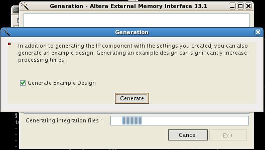
12 Creating the Example Design 10. After configuring the IP, click on Finish 11. A window will pop-up asking to create an example design Ensure the Generate Example Design option is selected and click on Generate 12
13 Interface IP and Example Design Output After IP generation is complete, <variation_name>_example_design directory will be created in your project directory In this example, the variation name is ddr3 and the script files needed to create an example design are available in ddr3_example_design 13
14 Two TCL Scripts Created <variation_name>_example_design contains two TCL scripts: I. make_qii_design.tcl The make_qii_design.tcl generates a synthesizable design example along with a Quartus project, ready for compilation II. make_sim_design.tcl The make_sim_design.tcl generates a simulation design example along with tool-specific scripts to compile and elaborate the necessary files 14
15 Generating the Example Design Files To generate synthesizable design example, run the make_qii_design.tcl script in Nios II command shell or from a command line: 12. Open Nios II command shell and browse to the <variation_name>_example_design directory Or change directory to <variation_name>_example_design directory 13. Run the make_qii_design.tcl script by executing the following command: quartus_sh -t make_qii_design.tcl Optionally can run the make_qii_design.tcl script for a specific device quartus_sh -t make_qii_design.tcl 10AX115R3F40I2SGES 15

16 Example Design Script Output This script runs for a few seconds and produces a qii directory containing a project called ed_synth.qpf Open and compile this project with the Quartus II software v13.1 Arria 10 Edition QSYS file is also generated Open this file in QSYS to add remove or modify IPs in the example design 16
17 Generating Simulation Files for Example Design Project Overview Details in simulation guidelines section 17

18 Memory Model Generating the Simulation Design Example Files To generate a simulation design example, run the following script in Nios II command shell or from the command line Options of VERILOG or VHDL quartus_sh -t make_sim_design.tcl VERILOG The simulation design example is made of a driver connected to the generated IP (device under test or DUT) and to the memory model Driver generates random traffic and internally checks the legality of the outgoing data Example Testbench Memory PHY AFI Avalon Driver (Traffic Controller Generator) Pass/Fail Arria 10 EMIF IP Core Example Design 18
19 Simulation Example Design Script Output Script creates a sim directory containing one subdirectory for each supported simulation tools Each subdirectory contains the specific scripts to run simulation with the corresponding tool 19
20 Arria 10 Simulation Guidelines Arria 10 Simulation Guidelines are preliminary and subject to change 20
21 Simulation Users will be able to choose between two simulation models Skip Calibration Fastest simulation Loads the settings calculated from memory configuration and enters user mode Full Calibration (not supported in Quartus II 13.1) Performs all stages of memory calibration: calibration phases, delay sweeps, and centering of all data bits Skip Calibration mode Full Calibration mode System-level simulation focusing on user logic Details of calibration are not captured Enables users to store and retrieve data Memory interface simulation focusing on calibration Details of calibration are captured (i.e. stages) Includes leveling, per-bit deskew, etc.. Efficiency accurate No board skews are taken into account 21
22 Simulation: Supported & Not Supported Supported Functional Verification Skip Calibration (default) Not Supported Timing Verification Nativelink Memory Vendor Models Full Calibration* Post-Fit Simulation* Multi-Rank* Multiple-CS memory interface* Memory frequency < 400Mhz* RDIMM & LRDIMM configurations* *Available in a future Quartus II version Note: Validating the timing of your design requires using Altera s TimeQuest Timing Analyzer 22
23 Simulation To simulate your design you will need the following components Altera Supported Simulator Design using Altera External Memory Interfaces IP An Example Driver (Altera or User) Testbench (Altera or User) Altera s Memory Simulation Model (We do not support simulation with memory vendor models) 23
24 Information About Simulation Filesets & Directory Core simulation filesets are identical to core synthesis filesets Addresses simulation v synthesis fileset concerns of the past Ensure users are simulating the blocks they are synthesizing <dut>/* <dut>_sim/altera_emif_arch_nf/* Any changes made in the synthesis directory should also be made in the simulation directory to reflect similar IP behavior Fewer files to compile for simulation compared to the External Memory Interfaces IP of the past (UniPHY, ALTMEMPHY) 64 files for the example design 7 are unique for each interface Users can modify the BIST in the example design if needed 24
25 Important Assumptions Made by Simulation Altera library simulation atoms assume the following: RTL simulation assumes an ideal layout including: Interfaces are unaware of each other Interface assumes it is the only interface in the column Interface believes it has its own IOAUX and Hard Nios Interface is at the bottom of the column, nearest to the physical IOAUX block location Fitter may actually place an interface at the top of the column if left unconstrained but there are no drawbacks between an interface at the top of the column and an interface at the bottom of the column One PLL per interface At Post-Fit, it is possible for interfaces to share the same bank PLL PLL reset only occur during power-up Issue a recalibration request per-emif interface in place of a PLL reset *EMIF = External Memory Interfaces 25

26 RTL Simulation v Post-Fit Implementation There may be a discrepancy between the simulated latency versus the Post-Fit latency Do not rely on the simulated interface latency bank 1 Lane 3 Lane 2 Lane 1 Lane 0 bank 0 Lane 3 Lane 2 Lane 1 Lane 0 RTL Simulation Fitter Operations bank 1 Lane 3 Lane 2 Lane 1 Lane 0 bank 0 Lane 3 Lane 2 Lane 1 Lane 0 Post-Fit Implementation AFI Clock Cycle Penalty 26

27 RTL Simulation v Post-Fit Implementation Introduction of AFI Clock Cycle penalty: For wide, multi-bank interfaces and/or ultra-low latency interfaces Fitter can detect this penalty and will issue a warning accordingly Only an issue when the requested write latency is less than the latency accrued by the farthest away bank bank 2 Lane 3 Lane 2 Lane 1 Lane 0 bank 1 Lane 3 Lane 2 Lane 1 Lane 0 bank 0 Lane 3 Lane 2 Lane 1 Lane 0 AFI Clock Cycle Penalty 27
28 RTL Simulation v Post-Fit Implementation RTL Simulation: NIOS initialization and calibration code executes in parallel for all interfaces Interfaces might assert cal_done (calibration done) simultaneously in simulation Do not rely on this behavior shown in simulation Post-Fit Implementation: NIOS initialization and calibration code executes sequentially Order of calibration is determined by fitter operations Calibration is complete when all interfaces in a column assert 'cal_done'" You must sample all cal_done signals in a column to determine when calibration is complete 28


29 Generating the Example Design Step 1: Generate the Design 29
30 Simulating the example design Generation Output File/Directory dut/ Description <- Actual IP for your project dut/ dut_example_design/ Actual IP for your <- Example project Design Subfolder dut_example_design/ dut_sim/ Example Design <- Subfolder Simulation fileset only (no driver, etc) dut.cmp dut_sim/ Simulation Fileset (no driver) dut.qip dut.cmp dut.spd Component Declaration File (text file containing port definitions that can be used in VHDL Design dut.sip Files) dut.qip dut.ppf dut.v Quartus IP File (contains paths for all files needed for the IP core) dut.spd Simulation Package Descriptor File (lists the required simulation files for the IP core or Qsys system) dut.sip Simulation IP File (contains information assignments that specify IP simulation source files) dut.ppf dut.v Pin Planner File (XML file that stores the port and node assignments for use with the Pin Planner) Variation File of the IP core (contains the IP settings used to generate the IP core) Core files in each subdirectory are identical dut_example_design/*: Contains driver and memory model dut_sim/* and dut/*: Identical 30
31 Example Design Output Files In dut_example_design File ed_sim.qsys ed_synth.qsys make_qii_design.tcl Description Qsys file capturing the simulation example design Qsys file capturing the example design for synthesis Script to generate the example design project for synthesis make_sim_design.tcl Script to generate the example design for simulation params.tcl params.txt readme.txt Support file for the generation scripts XML file created that holds user chosen IP settings Instructions for user 31
32 Generating the Example Design Simulation Files Run quartus_sh -t make_sim_design.tcl VERILOG to generate the simulation files for the example design in verilog Run quartus_sh -t make_sim_design.tcl VHDL to generate the simulation files for the example design in VHDL 32
33 Modelsim Example Flow You can create your own.do file in order to view signals in Modelsim s waveform viewer Example: run.do Execute do run.do in the Modelsim console to run the simulation with signal waveforms To only see a successful simulation result shown in the console messages Execute source msim_setup.tcl in the Modelsim console Execute ld_debug after msim_setup.tcl is loaded Execute run -all after ld_debug finishes 33
34 Modelsim Example Guide To store the entire log of the simulation data and results Edit msim_setup.tcl & add -l ed_sim.log to the vsim line 34
35 Simulating the example design Supported simulators: Supported Mentor Graphics Modelsim Synopsys VCS and VCS-MX Not Supported Aldec Riviera-PRO* Cadence NCSIM* *Available in a future Quartus II version 35
36 Arria 10 EMIF Timing Closure Guidelines Arria 10 timing closure guidelines are preliminary and subject to change

37 Arria 10 EMIF Timing paths User Logic (Core) Periphery IO including read, write, write levelling, etc 37
38 Timing Closure Guidelines Timing closure in any core transfers include From last set of registers in core to first set of registers to periphery (C2P) From last set of registers in periphery to first of registers in core (P2C) Note that C2P/P2C paths are cut and not analyzed in the current Quartus II release Core Timing analysis will not include user logic timing nor user logic timing to/from EMIF block Arria 10 timing analysis will not show any periphery-to-periphery timing in TimeQuest Timing closure in any of the IO transfers Not dependent on Quartus II compile Dependent on customer memory, FPGA speed grade parameters and channel effects For accurate timing analysis, simulate correct board parameters and channel effects Board skews must be simulated using board tool (not estimated or calculated via trace length) Channel effects (ISI and crosstalk) can only be determined by a board simulator Include simulated Board skew and Channel effects in Megawizard GUI during IP generation Refer to Board guidelines for more details on board skew and channel effects ReportDDR will run automatically as part of signoff timing analysis User has to check ReportDDR as part of signoff timing analysis to make sure EMIF has closed timing 38

39 Estimate Early IO Timing without Quartus II Compilation Users can see IO margins without compiling EMIF design Early IO timing will look like a spreadsheet type analysis shown in a TimeQuest panel Provides breakdown in margin loss between receiver/transmitter/channel Flow Generate EMIF IP with configuration of interest including memory and board parameters Create Quartus II project files ( QPF, QSF) with selected Arria 10 device part Run TimeQuest with <name>_report_io_timing.tcl that get s generated as part of the IP Details in the next slide EMIF IP generation EMIF source (.tcl files) Ideal Window Channel Effects Quartus project creation (including part selection) Quartus project files (.qpf/.qsf) Run _report_io_timing.tcl in TimeQuest Memory (Receiver) Effects FPGA (Transmitter) Effects Final Margin Early IO estimate flow Time Quest Panel 39


 Note: To generate early IO timing reports, run")
40 Running TimeQuest for Early IO Estimates 1. Start TimeQuest 2. Open Project 3. Pick Script Run TCL script 4. Pick <name>_report_io_timing.tcl file 5. TimeQuest prints out summary and creates a ReportDDR panel Same level of detail for IOs Produces a warning mentioning that core timing is not included Similar type of analysis available for all IO transfers (Read capture, DQS gating, A/C and Write Leveling) Note: To generate early IO timing reports, run report_io_timing.tcl before running any Quartus II compilation 40

41 Early IO Estimates other Execution Methods Instead of Script Run TCL script just type source <name>_report_io_timing.tcl in the TCL console OR At the command prompt type Quartus_sta -t <core_name>_report_io_timing.tcl <project_name> Note: Positive margins in Early IO timing estimate does not guarantee signoff timing analysis 41
42 Arria 10 Fitter Guidelines Arria 10 fitter guidelines are preliminary and subject to change 42
43 Fitter Behaviors Multi-bank Interface: Multiple, contiguous banks that make up one interface Introduction of AFI Clock Cycle penalty: For wide, multi-bank interfaces and/or ultra-low latency interfaces Fitter can detect this penalty and will issue a warning accordingly Only an issue when the requested write latency is less than the latency accrued by the farthest away bank in a multi-bank interface 43
44 Clocking Since multi-bank interfaces will use multiple PLLs and in turn multiple PHY clock trees, a reference clock tree will be used to route a common reference clock signal to all PLLs Not all pins can drive the PLL reference clock tree Quartus II software restricts PLL reference clock frequencies depending on the memory frequency Use the Arria 10 External Memory Interfaces IP Megawizard GUI to determine the valid PLL reference clock frequencies Fitter merges PLLs when a bank is shared by different interfaces Fitter duplicates PLL for multi-bank interfaces 44
45 Clocking Example of the reference clock tree driving multiple PLLs which are, in turn, driving multiple PHY clock trees Jitter is lowered with this balanced structure Balanced Reference Clock Network PLL PLL PLL PLL PHY clock tree PHY clock tree PHY clock tree PHY clock tree 45
46 Sharing Resources In Arria 10, the following resources can be shared and in some cases are forced to be share: *More in Pin Guidelines Certain resources are forced to be shared Resource I/O bank Hard Nios II Core Clock Network PLL reference clock pins* OCT block and RZQ pin* Address/Command pins* Implication Ability to fit more interfaces in a single column Cannot rely on one cal_done signal as representative of all interfaces passing the calibration stage Shared PLL reference network. Users should place interfaces in consecutive banks Shared PLL reference clock and network trees IOAUX & Hard Nios II CPU for all interfaces in a column A bank shared by two interfaces PLL/DLL do not need to be shared as each bank has one None Shared for Ping Pong PHY 46
47 Sharing an I/O Bank Fitter can place interfaces in a shared bank if the interfaces share the same: Protocol Rate Phase Frequency Users can fit even more interfaces in a column Interfaces cannot share the same controller nor sequencer Fitter will not allow users to have a lane shared by two interfaces One DQS-in tree can only talk to one controller Unused pins can be used by the customer as a GPIO Must be the same voltage standard 47
 Bank N+1 Fixed Address / Command Pin")

48 Example: 2 x16 interfaces sharing a bank Unused (Free for GPIO, but not LVDS) Bank N+1 Fixed Address / Command Pin out Data path Bank N Unused (Free for GPIO, but not LVDS) Data path Data path Bank N-1 Fixed Address / Command Pin out 48
49 Sharing Hard Nios / IOAUX Interfaces placed within the same column by the fitter will share the same IOAUX and Hard Nios II The Hard Nios II calibrates each interface sequentially You must sample all cal_done signals in a column to determine when calibration is complete RTL simulation behaves as if every interface has its own Hard Nios II More on this in the Simulation Design Guidelines 49
50 Sharing Hard Nios II Processor The Arria 10 External Memory Interfaces IP will contain one Hard Nios II and IOAUX per interface but fitter will merge them all into a single instance You must use the same IOAUX clock and reset for all interfaces in the same column or Fitter will generate an error IOAUX bank 3 Lane 3 Lane 2 Lane 1 Lane 0 bank 2 Lane 3 Lane 2 Lane 1 Lane 0 bank 1 Lane 3 Lane 2 Lane 1 Lane 0 50 bank 0 Lane 3 Lane 2 Lane 1 Lane 0
51 Sharing Core Clock Networks Fitter can use one core clock domain to synchronously access all interfaces in a column Users can share core clock networks by the master & slave setting in the IP generation GUI Connect core_clks_master_out from the master to all slave s core_clks_slave_in Must use same column, PLL reference clock, rate, and frequency Interfaces in different columns cannot use this feature Place interfaces in consecutive banks as the PLL reference clock are forced to be shared when choosing to share core clock networks 51
52 Fitter Relationship to Pin Assignments Pin assignments Fitter can reallocate banks based on user pin assignments Fitter can rotate pins within a lane based on user pin assignments but cannot move pins across lanes away from their DQS group Users can constrain a DQS pin to a lane, and the Fitter will place all DQ signals in their respective DQS group in the same lane 52
53 Arria10 Interface Pin Guidelines Arria 10 Pin Guidelines are preliminary and subject to change
54 Overview Pin Guidelines Guidelines Rules for constraining pins Determine IO bank requirements for DDR3, DDR4 Interface placement Find pin names for A/C and data pins Example for constraining DDR3 x8 and x72 Alternate methods for constraining interface pin assignments Pin guidelines for sharing multiple interfaces Constraints for sharing multiple interfaces Step by step guidelines 54
55 Pin Guidelines 1. Determine number of banks based on interface width 2. Pick CK0 pin based on desired interface location in the FPGA 3. Constrain CK0 pin to selected pin name or A/C bank 4. Constrain one DQS pin for each DQS group either to pin name or A/C bank 5. Constrain PLL reference clock pin and RZQ pin to pin names 55
56 Rules for constraining pins A/C All A/C pins should be in a single BANK A/C and data pins cannot share a lane (12 IOs) But unused A/C pins in a lane can be used by GPIOs A/C pins must follow predefined locations within a BANK A/C and data pins can share a bank DQ pins DQ signals from two different DQS groups cannot be constrained to same IO_12_LANE DQS pins Related DQ pins must be in the same IO_12_LANE(s) A read data group must be assigned based on DQSin grouping in pin table 56

57 Rules for constraining pins (contd) PLL Reference Clock pins For a given interface speed, there is a restriction on values of possible PLL ref clock frequencies Must use Arria 10 Interface v13.1 MegaWizard to determine possible PLL reference clock frequencies for onboard crystal oscillator Altera recommends using the default PLL reference clock frequency from MegaWizard Crystal clock frequency is generally lowest clock frequency of memory interface divided by integer N Where N= 1,2,3,4,5 Find detailed step by step guidelines for constraining pins in next few slides 57
58 DDR3: Determine Number of Banks Required Find number of banks required based on whether there is any IO bank sharing or not Pin count for DDR3 8/16/32-bit is based on 1CS When using multiple CS for DDR3 8/16/32-bit, Add 5 more pins for 2CS to total IO count Add 15 more pins for 4CS to total IO count Calculate the number of banks required with multiple CS pins No. of IO Banks = (Total No. of IOs for 1CS + Additional IOs for multiple CS) / 48 Interface width and memory configuration Number of IOs IO Banks (non-sharing) IO Banks sharing with other Interfaces (1/4 Granularity) 8-bit w/o ECC 1CS bit w/o ECC 1CS bit with ECC 1CS bit w/o ECC 1CS bit with ECC 1CS bit UDIMM 1-Rank bit UDIMM 2-Rank bit UDIMM 4-Rank bit SO-DIMM 1-Rank bit SO-DIMM 2-Rank bit SO-DIMM 4-Rank
59 DDR4: Determine Number of Banks Required Find number of banks required based on whether there is any IO bank sharing or not Pin count for DDR3 8/16/32-bit is based on 1CS When using multiple CS for DDR3 8/16/32-bit, Add 5 more pins for 2CS to total IO count Add 15 more pins for 4CS to total IO count Calculate the number of banks required with multiple CS pins No. of IO Banks = (Total No. of IOs for 1CS + Additional IOs for multiple CS) / 48 Interface width and memory configuration Number of IOs IO Banks (non-sharing) IO Banks sharing with other Interfaces (With 1/4 Granularity) 8-bit w/o ECC 1CS bit w/o ECC 1CS bit with ECC 1CS bit w/o ECC 1CS bit with ECC 1CS bit UDIMM 1-Rank bit UDIMM 2-Rank bit UDIMM 4-Rank bit UDIMM 1-Rank bit UDIMM 2-Rank bit UDIMM 4-Rank
 must be")
60 Plan Interface Placement in Column Select consecutive banks out of 8 banks in a column and select middle bank for Address/command (A/C) pins (Must) In case of even number of banks, pick any one of the middle two A/C pins can take 3 or 4 IO lanes depending on memory topology and protocol When A/C requires only 3 IO lanes, only bottom 3 lanes (A/C 0,1, 2) must be used
61 DDR3: Find pin number for CK0 pin Pin No. Component, UDIMM, SO-DIMM Find pin number for CK0 pin based on the A/C lanes selected Examples: 61 Pin 8 corresponds to CK0 pin Pin 24 corresponds to PLL_clockin[0] Pin 26 corresponds to RZQ The pin number for A/C pins is also generated in project _readme.txt in Project /submodules/ folder Altera recommends using the project _readme.txt file to find the pin numbers for A/C pins CK3# 44 CK3 43 CK2# 42 CK2 41 CKE[3] 40 CKE[2] 39 ODT3 38 ODT2 37 CS[3] 36 CS[2] 35 BA[2] 34 BA[1] 33 BA[0] 32 CAS# 31 RAS# 30 A[15] 29 A[14] 28 A[13] 27 A[12] 26 RZQ 25 PLL_clockin[1] 24 PLL_clockin[0] 23 A[11] 22 A[10] 21 A[9] 20 A[8] 19 A[7] 18 A[6] 17 A[5] 16 A[4] 15 A[3] 14 A[2] 13 A[1] 12 A[0] 11 CK1# 10 CK1 9 CK0# 8 CK0 7 CKE[1] 6 CKE[0] 5 ODT1 4 ODT0 3 CS[1] 2 CS[0] 1 RESET# 0 WE#
62 DDR4: Find Pin Number for CK0 Pin Pin No. Component UDIMM Find pin number for CK0 pin based on the A/C lanes selected 62 Examples: Pin 8 corresponds to CK0 pin Pin 24 corresponds to PLL_clockin[0] Pin 26 corresponds to RZQ The Pin number for A/C pins is also generated in project _readme.txt in Project /submodules/ folder Altera recommends using the project _readme.txt file to find the pin numbers for A/C pins 47 CK1# 46 CK1 45 CK3# 44 CK3 43 CK2# 42 CK2# 41 CKE[3] 40 CKE[2] 39 ODT3 38 ODT2 37 CS[3] 36 Alert_n CS[2] 35 BG[0] BG[0] 34 BA[1] BA[1] 33 BA[0] BA[0] 32 A[17] A[17] 31 A[16] A[16] 30 A[15] A[15] 29 A[14] A[14] 28 A[13] A[13] 27 A[12] A[12] 26 RZQ RZQ 25 PLL_clockin[1] PLL_clockin[1] 24 PLL_clockin[0] PLL_clockin[0] 23 A[11] A[11] 22 A[10] A[10] 21 A[9] A[9] 20 A[8] A[8] 19 A[7] A[7] 18 A[6] A[6] 17 A[5] A[5] 16 A[4] A[4] 15 A[3] A[3] 14 A[2] A[2] 13 A[1] A[1] 12 A[0] A[0] 11 PAR_in PAR_in 10 C2 CS[1] 9 CK0# CK0# 8 CK0 CK0 7 C1 CKE[1] 6 CKE[0] CKE[0] 5 C0 ODT1 4 ODT0 ODT0 3 ACT_n ACT_n 2 CS[0] CS[0] 1 RESET# RESET# 0 BG[1] BG[1]
63 Find Pin Name for CK0 and Constrain the Pin Based on A/C bank selected, identify column index and bank index for the A/C pins Column Index ranges from 0-1 and Bank Index from 0-7 Find pin name for A/C pin from pin table and constrain pin to pin name in QSF Example: Pin name for CK0 in Column0 Bank 6 is L23 set_location_assignment PIN_L23 to CK0 OR Find Bank name for A/C pin and constrain pin to selected IO48 bank in QSF Example: Selected IO bank for CK0 in Column0 Bank 6 is 2K set_location_assignment IOBANK_2K to CK0 Effectively locks all A/C signals Use Arria10 Pin table to find Pin index, Column index and Bank Index 63 I/O Bank P = Pin index (0-47) X = Column index Y = Bank index Pin name
64 Constrain DQS and PLL Reference Clock Pins Constrain PLL reference clock pin and RZQ pin to the pin names Constrain one DQS pin for each DQS group either to the pin names or selected IO48 banks Follow same method as CK0 for finding pin names for DQS and PLL reference clock pins Constraining CK0 pin, one DQS pin per group and PLL reference clock effectively locks the entire interface Good compromise between full-automatic and manual placement Requires minimal effort Altera recommends this method for constraining pin assignments 64
 set_location_assignment IOBANK_2A to DQS0 Constrain PLL_refclk to pin24 to Bank0 (P24X0Y0) set_location_assignment PIN_AM15 to")
65 Example for constraining DDR3 x8 Requires 1 Bank 3 lanes for A/C pins and 1 lane for DQ and DQS pins Picked IO lanes 0,1,2 for A/C Pins Constrain pin CK0 to pin8 of Bank0 (P8X0Y0) set_location_assignment PIN_AG16 to CK0 Constrain pin DQS0 to Bank0 (2A) set_location_assignment IOBANK_2A to DQS0 Constrain PLL_refclk to pin24 to Bank0 (P24X0Y0) set_location_assignment PIN_AM15 to PLL_clockin Constrain rzqpin to pin24 to Bank0 (P26X0Y0) set_location_assignment PIN_AK18 to rzqpin
 Constrain PLL refclk to pin24 of Bank1 (P24X0Y1)")
 DQS3 to Bank2 (2G) DQS4 to Bank1 (2F) DQS5 to Bank0 (2A) DQS6 to Bank0 (2A) DQS7 to Bank0 (2A) DQS8 to Bank0")
66 Example for constraining DDR3 x72 DDR3 x72 w/ Hard Controller Requires 3 banks 3 lanes for A/C pins 9 lanes for data Constraining DDR3 x72 Constrain pin CK0 to pin8 of Bank1 (P8X0Y1) Constrain PLL refclk to pin24 of Bank1 (P24X0Y1) Constrain rzqpin to pin26 of Bank1 (P24X0Y1) Constrain DQS groups DQS0 to Bank2 (2G) DQS1 to Bank2 (2G) DQS2 to Bank2 (2G) DQS3 to Bank2 (2G) DQS4 to Bank1 (2F) DQS5 to Bank0 (2A) DQS6 to Bank0 (2A) DQS7 to Bank0 (2A) DQS8 to Bank0 (2A) 66
67 Alternate Methods: Constraining Interface Pin assignments 1. Let the fitter assign all Interface signals (A/C, DQS, DQ pins) automatically a) Run the design through the fitter without any constraints b) Save the post-fit netlist, or back-annotate the pin assignments Requires least effort but longer compilation time This method works well for small designs (one interface per column) Must not use this method for darge designs with multiple IPs (Interfaces, HSSI, GPIOs, LVDS etc.) 2. Manually constrain all Interface signals (A/C, DQS, DQ pins) to pin locations a) Plan the Interface placement in a column (i.e., which IO48 banks to use) b) Use pin table to find legal position for each Interface pin c) Use QSF assignments to lock down the pins Fast periphery placement Can be a lengthy/tedious process (especially with multiple IPs) 67
68 Overview Pin Guidelines Step by Step Guidelines Rules for constraining A/C, DQ, DQS and CLK Pins Determine IO Bank Requirements for DDR3, DDR4 Interface placement Find Pin Names for A/C and data pins Constraining Interface Pin assignments Pin Guidelines for sharing Multiple Interfaces Constraints for sharing multiple interfaces Step by step guidelines 68
69 Constraints for Sharing Multiple Interfaces While sharing bank across multiple Interfaces the following criteria should be followed Must use identical clocks (rate, frequency, PLL ref clock) Same protocol Same voltage settings ( VCCIO, VREF) While sharing PLL Reference clock pin between interfaces the banks must be consecutive Interfaces using same IO standard can share OCT and RZQ Pin A bank cannot be used as A/C bank for two or more interfaces Reason: hard controller and sequencer cannot be shared A lane cannot be shared Reason: only one DQSin tree per lane; a lane can only talk to one controller 69
70 Pin Guidelines for Sharing Multiple Interfaces (Steps) 1. Determine total number of interfaces required 2. Determine No. of banks based on interface width and No. of interfaces 3. Ensure that interfaces meet the criteria for sharing interfaces 4. Plan Interface placement in column(s) a. Select middle bank for sharing DQ pins between two interfaces 5. For each interface, constrain CK pin to selected A/C bank or pin name 6. Constrain PLL reference clock to the A/C bank for one of the interfaces only 7. For each interface, constrain one DQS pin in each DQS group to a pin name or Bank. 70
71 Arria 10 Board Design Guidelines Arria 10 board design guidelines are preliminary and subject to change
72 Guidelines Following guidelines are covered in the subsequent slides and they apply to both DDR3 and DDR4 Generic guidelines Length DQ to DQS delay Address command (should include the package delay?) Delay within the group DQS to CK guideline Length matching guidelines are recommendations and they should not be considered as hard guidelines Customer must perform necessary board level simulation to make sure there are no signal integrity, ISI and crosstalk related issues Customers must also enter accurate information in the Board Timing tab of the memory MegaCore and compile the design to ensure there are no timing violations 72
73 Generic Guideline Trace impedance plays an important role in the signal integrity Users must perform board level simulation to determine the best characteristic impedance for their PCB For example, it is possible that for multi rank systems 40 ohm would yield better result than a traditional 50 ohm characteristic impedance To minimize PCB layer propagation variance, Altera recommend that you route signals from the same net group on the same layer Use 45 angles (not 90 corners) Disallow critical signals across split planes Route over appropriate VCC and GND planes Keep signal routing layers close to GND and power planes Avoid routing memory signals closer than inch (0.635 mm) to memory clocks 73
74 Maximum Lengths For DIMM From FPGA to DIMM connector max allowed trace length is 4.5 inches. Maximum DIMM to DIMM distance is inches For Discrete components 7 inches maximum for address/command signal 5 inches maximum for DQ/DQS/DM 74

75 DQ-DQS Delay Match the (package + board) trace delays up to 20 ps of skew for DQ/DQS/DM signals within a DQS group. Details on how to do package de-skew is available in EMIF HB vol2 chapter 4. 75
76 Address/Command/Control Skew All the address, command and control signals should match up to +/- 20 ps compare to the mem_clk trace For example if the mem_clk trace delay is 500 ps then the allowed range for any address/command/control signal is 480 ps to 520 ps For discrete components; make sure above recommendation is met for each component in the fly-by chain For DIMMs: For single or multiple DIMM configuration make sure this guideline is met at each DIMM connector 76
77 Address/Command/Control Skew x = y +/- 20 ps x + x1 = y + y1 +/- 20 ps x + x1 + x2 = y + y1 + y2 +/- 20 ps X + x1 + x2 + x3 = y + y1 + y2 + y3 +/- 20 ps 77
78 DQS-CLK guideline The timing between the DQS and clock signals on each device calibrates dynamically to meet tdqss. To make sure the skew is not too large for the leveling circuit s capability 1. Propagation delay of clock signal must not be shorter than propagation delay of DQS signal at every device: (CKi ) DQSi > 0; 0 < i < number of components 1 2. Total skew of CLK and DQS signal between groups is less than one clock cycle: (CKi + DQSi) max (CKi + DQSi) min < 1 tck If you are using a DIMM topology, your delay and skew must take into consideration values for the actual DIMM. 78
79 Simulation Guideline 1. Using board sim tool such as Hyperlynx, set up a trace models which includes IBIS/Hspice buffer models for FPGA and memory, DIMM connector model (if applicable) and accurate board stack up 2. Use this setup to extract accurate trace delay and ISI information 3. Export memory interface layout into the board sim tool to run the board level simulation 4. Use PDN analysis tools to simulate the power supply noise 79
80 Board Skew Parameters Users must enter accurate information about various delays and the skew in the MegaWizard Timing analysis DDR timing analysis scripts take board skews into account when generating timing analysis report Inaccurate board skew parameters with result in inaccurate timing analysis of the memory interface Delay Chain Settings Physical delays are applied to delay chains to compensate for the skew mismatch between various signals Board skew parameters affects the initial value applied to the delay chains Altera recommends that you simulate your interface in Hyperlynx (or similar tool) to acquire trace delays You can use the Board Skew Parameters Tool available on altera website to calculate the parameter once you have acquired the trace delays 80

81 Slew Rates, ISI and Crosstalk As the operating frequencies are pushing beyond 1 GHz, it is becoming increasingly important that user enters accurate slew rates and ISI/crosstalk information Customers should perform board simulation on the external memory interfaces and acquire all the necessary slew rates and ISI/crosstalk related information, and enter that information into the MegaWizard Do not use the default values. Accurate information about slew rates and ISI/crosstalk will result in accurate timing analysis of the interface Refer to EMIF HB Vol2 Chapter 9 for further information about Board Timing parameters 81

82 Thank You
Intel Stratix 10 External Memory Interfaces IP Design Example User Guide
 Intel Stratix 10 External Memory Interfaces IP Design Example User Guide Updated for Intel Quartus Prime Design Suite: 17.1 Subscribe Send Feedback Latest document on the web: PDF HTML Contents Contents
External Memory Interfaces Intel Arria 10 FPGA IP Design Example User Guide
 External Memory Interfaces Intel Arria 10 FPGA IP Design Example User Guide Updated for Intel Quartus Prime Design Suite: 18.0 Subscribe Send Feedback Latest document on the web: PDF HTML Contents Contents
Intel Cyclone 10 External Memory Interfaces IP Design Example User Guide
 Intel Cyclone 10 External Memory Interfaces IP Design Example User Guide Updated for Intel Quartus Prime Design Suite: 17.1 Subscribe Send Feedback Latest document on the web: PDF HTML Contents Contents
Interfacing DDR2 SDRAM with Stratix II, Stratix II GX, and Arria GX Devices
 Interfacing DDR2 SDRAM with Stratix II, Stratix II GX, and Arria GX Devices November 2007, ver. 4.0 Introduction Application Note 328 DDR2 SDRAM is the second generation of double-data rate (DDR) SDRAM
10. Simulating Memory IP
 10. Simulating Memory IP November 2012 EMI_DG_009-5.1 EMI_DG_009-5.1 This chapter describes the simulation basics so that you are aware of the supported simulators and options available to you when you
High Speed Memory Interfacing 800MHz DDR3 Memory Lab
 High Speed Memory Interfacing 800MHz DDR3 Memory Lab Software Requirements Overview 1) The Quartus II software version 11.1 2) Modelsim software version 11.1 This lab focuses on compiling and simulating
Intel Cyclone 10 External Memory Interfaces IP User Guide
 Intel Cyclone 10 External Memory Interfaces IP User Guide Updated for Intel Quartus Prime Design Suite: 17.1 Subscribe Send Feedback Latest document on the web: PDF HTML Contents Contents 1 Intel Cyclone
QDR II SRAM Board Design Guidelines
 8 emi_dg_007 Subscribe The following topics provide guidelines for you to improve your system's signal integrity and layout guidelines to help successfully implement a QDR II or QDR II+ SRAM interface
Intel Stratix 10 External Memory Interfaces IP User Guide
 Intel Stratix 10 External Memory Interfaces IP User Guide Updated for Intel Quartus Prime Design Suite: 17.1 Subscribe Send Feedback Latest document on the web: PDF HTML Contents Contents 1 Intel Stratix
SerialLite III Streaming IP Core Design Example User Guide for Intel Arria 10 Devices
 IP Core Design Example User Guide for Intel Arria 10 Devices Updated for Intel Quartus Prime Design Suite: 17.1 Subscribe Send Feedback Latest document on the web: PDF HTML Contents Contents 1 Quick Start
External Memory Interfaces Intel Arria 10 FPGA IP User Guide
 External Memory Interfaces Intel Arria 10 FPGA IP User Guide Updated for Intel Quartus Prime Design Suite: 18.0 Subscribe Send Feedback Latest document on the web: PDF HTML Contents Contents 1. External
AN 462: Implementing Multiple Memory Interfaces Using the ALTMEMPHY Megafunction
 AN 462: Implementing Multiple Memory Interfaces Using the ALTMEMPHY Megafunction April 2009 AN-462-1.3 Introduction Many systems and applications use external memory interfaces as data storage or buffer
SerialLite III Streaming IP Core Design Example User Guide for Intel Stratix 10 Devices
 SerialLite III Streaming IP Core Design Example User Guide for Intel Stratix 10 Devices Updated for Intel Quartus Prime Design Suite: 17.1 Stratix 10 ES Editions Subscribe Send Feedback Latest document
External Memory Interfaces Intel Stratix 10 FPGA IP User Guide
 External Memory Interfaces Intel Stratix 10 FPGA IP User Guide Updated for Intel Quartus Prime Design Suite: 18.0 Subscribe Send Feedback Latest document on the web: PDF HTML Contents Contents 1. External
Intel Stratix 10 MX HBM2 IP User Guide
 Intel Stratix 10 MX HBM2 IP User Guide Updated for Intel Quartus Prime Design Suite: 17.1 Subscribe Send Feedback Latest document on the web: PDF HTML Contents Contents 1 Introduction to High Bandwidth
DDR and DDR2 SDRAM Controller Compiler User Guide
 DDR and DDR2 SDRAM Controller Compiler User Guide 101 Innovation Drive San Jose, CA 95134 www.altera.com Operations Part Number Compiler Version: 8.1 Document Date: November 2008 Copyright 2008 Altera
ALTERA FPGAs Architecture & Design
 ALTERA FPGAs Architecture & Design Course Description This course provides all theoretical and practical know-how to design programmable devices of ALTERA with QUARTUS-II design software. The course combines
Intel FPGA PHYLite for Parallel Interfaces IP Core User Guide
 Intel FPGA PHYLite for Parallel Interfaces IP Core User Guide Updated for Intel Quartus Prime Design Suite: 17.1 Subscribe Send Feedback Latest document on the web: PDF HTML Contents Contents...3 Device
Intel FPGA GPIO IP Core User Guide
 Intel FPGA GPIO IP Core User Guide Updated for Intel Quartus Prime Design Suite: 17.1 Subscribe Send Feedback Latest document on the web: PDF HTML Contents Contents...3 Intel FPGA GPIO IP Core Features...
Implementing Multiple Memory Interfaces Using the ALTMEMPHY Megafunction
 Implementing Multiple Memory Interfaces Using the ALTMEMPHY Megafunction May 2008, v.1.2 Introduction Application Note 462 Many systems and applications use external memory interfaces as data storage or
High Bandwidth Memory (HBM2) Interface Intel FPGA IP User Guide
 Interface Intel FPGA IP User Guide") High Bandwidth Memory (HBM2) Interface Intel FPGA IP User Guide Updated for Intel Quartus Prime Design Suite: 18.0 Subscribe Send Feedback Latest document on the web: PDF HTML Contents Contents 1. Introduction
High Bandwidth Memory (HBM2) Interface Intel FPGA IP User Guide Updated for Intel Quartus Prime Design Suite: 18.0 Subscribe Send Feedback Latest document on the web: PDF HTML Contents Contents 1. Introduction
Arria 10 GX Dev kit 으로 PCI express 와 DDR4 완전정복. 송영규차장 Staff FAE, Altera Korea
 Arria 10 GX Dev kit 으로 PCI express 와 DDR4 완전정복 송영규차장 Staff FAE, Altera Korea Module Game Plan PCI EXPRESS OVERVIEW Performance, Productivity, & Features High-Performance DDR4 Interface Introduce DDR4 DDR4
MICROTRONIX AVALON MOBILE DDR MEMORY CONTROLLER IP CORE
 MICROTRONIX AVALON MOBILE DDR MEMORY CONTROLLER IP CORE USER MANUAL V1.6 126-4056 Meadowbrook Drive. London, ON Canada N5L 1E3 www.microtronix.com Document Revision History This user guide provides basic
External Memory Interfaces Intel Cyclone 10 GX FPGA IP User Guide
 External Memory Interfaces Intel Cyclone 10 GX FPGA IP User Guide Updated for Intel Quartus Prime Design Suite: 18.1 Subscribe Latest document on the web: PDF HTML Contents Contents 1. External Memory
Intel Stratix 10 H-tile Hard IP for Ethernet Design Example User Guide
 Intel Stratix 10 H-tile Hard IP for Ethernet Design Example User Guide Updated for Intel Quartus Prime Design Suite: 17.1 Subscribe Send Feedback Latest document on the web: PDF HTML Contents Contents
Low Latency 100G Ethernet Intel Stratix 10 FPGA IP Design Example User Guide
 Low Latency 100G Ethernet Intel Stratix 10 FPGA IP Design Example User Guide Updated for Intel Quartus Prime Design Suite: 18.0 Subscribe Send Feedback Latest document on the web: PDF HTML Contents Contents
Advanced ALTERA FPGA Design
 Advanced ALTERA FPGA Design Course Description This course focuses on advanced FPGA design topics in Quartus software. The first part covers advanced timing closure problems, analysis and solutions. The
11. Analyzing Timing of Memory IP
 11. Analyzing Timing of Memory IP November 2012 EMI_DG_010-4.2 EMI_DG_010-4.2 Ensuring that your external memory interface meets the various timing requirements of today s high-speed memory devices can
High Bandwidth Memory (HBM2) Interface Intel FPGA IP Design Example User Guide
 Interface Intel FPGA IP Design Example User Guide") High Bandwidth Memory (HBM2) Interface Intel FPGA IP Design Example Updated for Intel Quartus Prime Design Suite: 18.1.1 Subscribe Latest document on the web: PDF HTML Contents Contents 1. High Bandwidth
High Bandwidth Memory (HBM2) Interface Intel FPGA IP Design Example Updated for Intel Quartus Prime Design Suite: 18.1.1 Subscribe Latest document on the web: PDF HTML Contents Contents 1. High Bandwidth
Analyzing Timing of Memory IP
 11 emi_dg_010 Subscribe The external memory physical layer (PHY) interface offers a combination of source-synchronous and self-calibrating circuits to maximize system timing margins. The physical layer
2. Recommended Design Flow
 2. Recommended Design Flow This chapter describes the Altera-recommended design low or successully implementing external memory interaces in Altera devices. Altera recommends that you create an example
Arria 10 Migration Guide
 Arria 10 Migration Guide Subscribe UG-01149 101 Innovation Drive San Jose, CA 95134 www.altera.com TOC-2 Arria 10 Migration Guide Contents ACDS 13.1 Arria 10 Edition Known Issues...1-1 Device Support for
JESD204B Intel Cyclone 10 GX FPGA IP Design Example User Guide
 JESD204B Intel Cyclone 10 GX FPGA IP Design Example User Guide Updated for Intel Quartus Prime Design Suite: 18.0 Subscribe Send Feedback Latest document on the web: PDF HTML Contents Contents 1. JESD204B
Quartus II Software Version 11.1 Release Notes
 Quartus II Software Version 11.1 Release Notes RN-01069-1.0 Release Notes This document provides late-breaking information about the following areas of the Altera Quartus II software version 11.1. New
H-tile Hard IP for Ethernet Intel Stratix 10 FPGA IP Design Example User Guide
 H-tile Hard IP for Ethernet Intel Stratix 10 FPGA IP Design Example User Guide Updated for Intel Quartus Prime Design Suite: 18.0 Subscribe Send Feedback Latest document on the web: PDF HTML Contents Contents
Intel Quartus Prime Pro Edition Software and Device Support Release Notes
 Intel Quartus Prime Pro Edition Software and Device Support Release Notes RN-01082-17.0.0 2017.05.08 Subscribe Send Feedback Contents Contents 1 Version 17.0... 3 1.1 New Features and Enhancements...3
DDR and DDR2 SDRAM High-Performance Controller User Guide
 DDR and DDR2 SDRAM High-Performance Controller User Guide 101 Innovation Drive San Jose, CA 95134 (408) 544-7000 www.altera.com Operations Part Number MegaCore Version: 8.0 Document Version: 8.0 Document
9. Functional Description Example Designs
 November 2012 EMI_RM_007-1.3 9. Functional Description Example Designs EMI_RM_007-1.3 This chapter describes the example designs and the traffic generator. Two independent example designs are created during
25G Ethernet Intel Stratix 10 FPGA IP Design Example User Guide
 25G Ethernet Intel Stratix 10 FPGA IP Design Example User Guide Updated for Intel Quartus Prime Design Suite: 18.0 Subscribe Send Feedback Latest document on the web: PDF HTML Contents Contents 1. 25G
DDR3 SDRAM High-Performance Controller User Guide
 DDR3 SDRAM High-Performance Controller User Guide 101 Innovation Drive San Jose, CA 95134 www.altera.com Operations Part Number MegaCore Version: 8.0 Document Date: May 2008 Copyright 2008 Altera Corporation.
Arria 10 JESD204B IP Core Design Example User Guide
 Arria 10 JESD204B IP Core Design Example User Guide UG-DEX-A10-JESD204B 2017.05.08 Last updated for Intel Quartus Prime Design Suite: 17.0 Subscribe Send Feedback Contents Contents 1 Arria 10 JESD204B
8. Best Practices for Incremental Compilation Partitions and Floorplan Assignments
 8. Best Practices for Incremental Compilation Partitions and Floorplan Assignments QII51017-9.0.0 Introduction The Quartus II incremental compilation feature allows you to partition a design, compile partitions
DDR & DDR2 SDRAM Controller Compiler
 DDR & DDR2 SDRAM Controller Compiler August 2007, Compiler Version 7.1 Errata Sheet This document addresses known errata and documentation issues for the DDR and DDR2 SDRAM Controller Compiler version
DDR4 Design And Verification In Hyperlynx LINESIM/Boardsim
 DDR4 Design And Verification In Hyperlynx LINESIM/Boardsim Rod Strange Business Development Manager Teraspeed Consulting A Division of Samtec April 2016 Outline Objective/Goal DDR4 vs. DDR3 from the SI/PI
Cover TBD. intel Quartus prime Design software
 Cover TBD intel Quartus prime Design software Fastest Path to Your Design The Intel Quartus Prime software is revolutionary in performance and productivity for FPGA, CPLD, and SoC designs, providing a
Intel Stratix 10 Low Latency 40G Ethernet Design Example User Guide
 Intel Stratix 10 Low Latency 40G Ethernet Design Example User Guide Updated for Intel Quartus Prime Design Suite: 18.1 Subscribe Latest document on the web: PDF HTML Contents Contents 1. Quick Start Guide...
External Memory Interface Handbook
 External Memory Interface Handbook Volume 3: Reference Material Last updated for Altera Complete Design Suite: 14.1 Subscribe EMI_RM 101 Innovation Drive San Jose, CA 95134 www.altera.com TOC-2 External
Tutorial for Altera DE1 and Quartus II
 Tutorial for Altera DE1 and Quartus II Qin-Zhong Ye December, 2013 This tutorial teaches you the basic steps to use Quartus II version 13.0 to program Altera s FPGA, Cyclone II EP2C20 on the Development
AN 756: Altera GPIO to Altera PHYLite Design Implementation Guidelines
 AN 756: Altera GPIO to Altera PHYLite Design Implementation Guidelines AN-756 2017.05.08 Subscribe Send Feedback Contents Contents 1...3 1.1 Implementing the Altera PHYLite Design... 3 1.1.1 Parameter
Quartus II Software Version 10.0 SP1 Device Support
 Quartus II Software Version 10.0 SP1 Device Support RN-01057 Release Notes This document provides late-breaking information about device support in the 10.0 SP1 version of the Altera Quartus II software.
ALTERA FPGA Design Using Verilog
 ALTERA FPGA Design Using Verilog Course Description This course provides all necessary theoretical and practical know-how to design ALTERA FPGA/CPLD using Verilog standard language. The course intention
Cover TBD. intel Quartus prime Design software
 Cover TBD intel Quartus prime Design software Fastest Path to Your Design The Intel Quartus Prime software is revolutionary in performance and productivity for FPGA, CPLD, and SoC designs, providing a
2. SDRAM Controller Core
 2. SDRAM Controller Core Core Overview The SDRAM controller core with Avalon interface provides an Avalon Memory-Mapped (Avalon-MM) interface to off-chip SDRAM. The SDRAM controller allows designers to
Design Flow Tutorial
 Digital Design LU Design Flow Tutorial Jakob Lechner, Thomas Polzer {lechner, tpolzer}@ecs.tuwien.ac.at Department of Computer Engineering University of Technology Vienna Vienna, October 8, 2010 Contents
Managing Quartus II Projects
 1 QII52012 Subscribe The Quartus II software organizes and manages the elements of your design within a project. The project encapsulates information about your design hierarchy, libraries, constraints,
System Debugging Tools Overview
 9 QII53027 Subscribe About Altera System Debugging Tools The Altera system debugging tools help you verify your FPGA designs. As your product requirements continue to increase in complexity, the time you
100G Interlaken MegaCore Function User Guide
 00G Interlaken MegaCore Function User Guide Subscribe UG-028 05.06.203 0 Innovation Drive San Jose, CA 9534 www.altera.com TOC-2 00G Interlaken MegaCore Function User Guide Contents About This MegaCore
External Memory Interface Handbook Volume 2 Section I. Device and Pin Planning
 External Memory Interface Handbook Volume 2 Section I. Device and Pin Planning External Memory Interface Handbook Volume 2 101 Innovation Drive San Jose, CA 95134 www.altera.com EMI_PLAN_PIN-3.0 Document
Fixed-Point IP Cores (ALTERA_FIXED- POINT_FUNCTIONS) User Guide
 User Guide") Fixed-Point IP Cores (ALTERA_FIXED- POINT_FUNCTIONS) User Guide UG-20067 2017.03.31 Subscribe Send Feedback Contents Contents 1 About Fixed-Point IP Cores... 3 2 Getting Started... 4 2.1 Installing and
Fixed-Point IP Cores (ALTERA_FIXED- POINT_FUNCTIONS) User Guide UG-20067 2017.03.31 Subscribe Send Feedback Contents Contents 1 About Fixed-Point IP Cores... 3 2 Getting Started... 4 2.1 Installing and
QDRII SRAM Controller MegaCore Function User Guide
 QDRII SRAM Controller MegaCore Function User Guide 101 Innovation Drive San Jose, CA 95134 www.altera.com MegaCore Version: 9.1 Document Date: November 2009 Copyright 2009 Altera Corporation. All rights
Debugging Transceiver Links
 Debugging s 11 QII53029 Subscribe This chapter describes using the Transceiver Toolkit to optimize high-speed serial links in your board design. The Transceiver Toolkit provides real-time control, monitoring,
DE2 Board & Quartus II Software
 January 23, 2015 Contact and Office Hours Teaching Assistant (TA) Sergio Contreras Office Office Hours Email SEB 3259 Tuesday & Thursday 12:30-2:00 PM Wednesday 1:30-3:30 PM contre47@nevada.unlv.edu Syllabus
Interlaken IP Core (2nd Generation) Design Example User Guide
 Design Example User Guide") Interlaken IP Core (2nd Generation) Design Example User Guide UG-20051 2017.09.19 Subscribe Send Feedback Contents Contents 1 Quick Start Guide... 3 1.1 Directory Structure... 4 1.2 Design Components...
Interlaken IP Core (2nd Generation) Design Example User Guide UG-20051 2017.09.19 Subscribe Send Feedback Contents Contents 1 Quick Start Guide... 3 1.1 Directory Structure... 4 1.2 Design Components...
Xilinx Answer MIG 7 Series DDR3/DDR2 - Hardware Debug Guide
 Xilinx Answer 43879 MIG 7 Series DDR3/DDR2 - Hardware Debug Guide Important Note: This downloadable PDF of an Answer Record is provided to enhance its usability and readability. It is important to note
8. Introduction to UniPHY IP
 8. Introduction to Uni IP November 2011 EMI_RM_008-1.1 EMI_RM_008-1.1 The Altera and SDRAM controllers with Uni, QDR II and QDR II+ SRAM controllers with Uni, and RLDRAM II controller with Uni provide
AN 812: Qsys Pro System Design Tutorial
 AN 812: Qsys Pro System Design Tutorial AN-812 2017.08.15 Subscribe Send Feedback Contents Contents Qsys Pro System Design Tutorial... 3 Hardware and Software Requirements... 4 Download and Install the
7. External Memory Interfaces in Arria II Devices
 ecember 2010 AIIGX51007-4.0 7. External Memory Interfaces in Arria II evices AIIGX51007-4.0 This chapter describes the hardware features in Arria II devices that facilitate high-speed memory interfacing
June 2003, ver. 1.2 Application Note 198
 Timing Closure with the Quartus II Software June 2003, ver. 1.2 Application Note 198 Introduction With FPGA designs surpassing the multimillion-gate mark, designers need advanced tools to better address
Best Practices for Incremental Compilation Partitions and Floorplan Assignments
 Best Practices for Incremental Compilation Partitions and Floorplan Assignments December 2007, ver. 1.0 Application Note 470 Introduction The Quartus II incremental compilation feature allows you to partition
Interfacing RLDRAM II with Stratix II, Stratix,& Stratix GX Devices
 Interfacing RLDRAM II with Stratix II, Stratix,& Stratix GX Devices November 2005, ver. 3.1 Application Note 325 Introduction Reduced latency DRAM II (RLDRAM II) is a DRAM-based point-to-point memory device
External Memory Interfaces in Cyclone V Devices
 External Memory Interfaces in Cyclone V Devices..8 CV-5 Subscribe Feedback The Cyclone V devices provide an efficient architecture that allows you fit wide external memory interfaces support a high level
Quartus II Software Version 11.1 SP1 Release Notes
 Quartus II Software Version 11.1 SP1 Release Notes RN-01070-1.0 Release Notes This document provides late-breaking information about the following areas of the Altera Quartus II software version 11.1 SP1.
Intel Stratix 10 General Purpose I/O User Guide
 Intel Stratix 10 General Purpose I/O User Guide Updated for Intel Quartus Prime Design Suite: 18.0 Subscribe Send Feedback Latest document on the web: PDF HTML Contents Contents 1. Intel Stratix 10 I/O
2. Mentor Graphics ModelSim and QuestaSim Support
 November 2012 QII53001-12.1.0 2. Mentor Graphics ModelSim and QuestaSim Support QII53001-12.1.0 This chapter provides specific guidelines for simulation of Quartus II designs with Mentor Graphics ModelSim-Altera,
Phase-Locked Loop Reconfiguration (ALTPLL_RECONFIG) Megafunction
 Megafunction") Phase-Locked Loop Reconfiguration (ALTPLL_RECONFIG) Megafunction UG-032405-6.0 User Guide This user guide describes the features and behavior of the ALTPLL_RECONFIG megafunction that you can configure
Phase-Locked Loop Reconfiguration (ALTPLL_RECONFIG) Megafunction UG-032405-6.0 User Guide This user guide describes the features and behavior of the ALTPLL_RECONFIG megafunction that you can configure
Low Latency 100G Ethernet Design Example User Guide
 Low Latency 100G Ethernet Design Example User Guide Updated for Intel Quartus Prime Design Suite: 16.1 Subscribe Send Feedback Latest document on the web: PDF HTML Contents Contents 1 Quick Start Guide...
QDRII SRAM Controller MegaCore Function User Guide
 QDRII SRAM Controller MegaCore Function User Guide 101 Innovation Drive San Jose, CA 95134 www.altera.com MegaCore Version: 8.1 Document Date: November 2008 Copyright 2008 Altera Corporation. All rights
DDR & DDR2 SDRAM Controller Compiler
 DDR & DDR2 SDRAM Controller Compiler march 2007, Compiler Version 7.0 Errata Sheet This document addresses known errata and documentation issues for the DDR and DDR2 SDRAM Controller Compiler version 7.0.
Intel Quartus Prime Pro Edition
 Intel Quartus Prime Pro Edition Version 18.1 Software and Device Support Release Notes Subscribe Latest document on the web: PDF HTML Contents Contents 1. Intel Quartus Prime Pro Edition Version 18.1 Software
Dynamic Reconfiguration of PMA Controls in Stratix V Devices
 Dynamic Reconfiguration of PMA Controls in Stratix V Devices AN-645-1.0 Application Note This application note describes how to use the transceiver reconfiguration controller to dynamically reconfigure
7. External Memory Interfaces in Stratix IV Devices
 February 2011 SIV51007-3.2 7. External Memory Interfaces in Stratix IV evices SIV51007-3.2 This chapter describes external memory interfaces available with the Stratix IV device family and that family
2.5G Reed-Solomon II MegaCore Function Reference Design
 2.5G Reed-Solomon II MegaCore Function Reference Design AN-642-1.0 Application Note The Altera 2.5G Reed-Solomon (RS) II MegaCore function reference design demonstrates a basic application of the Reed-Solomon
1. SDRAM Controller Core
 1. SDRAM Controller Core NII51005-7.2.0 Core Overview The SDRAM controller core with Avalon interface provides an Avalon Memory-Mapped (Avalon-MM) interface to off-chip SDRAM. The SDRAM controller allows
MICROTRONIX AVALON MULTI-PORT SDRAM CONTROLLER
 MICROTRONIX AVALON MULTI-PORT SDRAM CONTROLLER USER MANUAL V3.11 126-4056 Meadowbrook Drive London, ON Canada N5L 1E3 www.microtronix.com Document Revision History This user guide provides basic information
13. LogicLock Design Methodology
 13. LogicLock Design Methodology QII52009-7.0.0 Introduction f Available exclusively in the Altera Quartus II software, the LogicLock feature enables you to design, optimize, and lock down your design
10. Introduction to UniPHY IP
 10. Introduction to Uni IP November 2012 EMI_RM_008-2.1 EMI_RM_008-2.1 The Altera,, and LP SDRAM controllers with Uni, QDR II and QDR II+ SRAM controllers with Uni, RLDRAM II controller with Uni, and RLDRAM
AN 567: Quartus II Design Separation Flow
 AN 567: Quartus II Design Separation Flow June 2009 AN-567-1.0 Introduction This application note assumes familiarity with the Quartus II incremental compilation flow and floorplanning with the LogicLock
Low Latency 40G Ethernet Example Design User Guide
 Low Latency 40G Ethernet Example Design User Guide Subscribe UG-20025 101 Innovation Drive San Jose, CA 95134 www.altera.com TOC-2 Contents Quick Start Guide...1-1 Directory Structure... 1-2 Design Components...
8. Migrating Stratix II Device Resources to HardCopy II Devices
 8. Migrating Stratix II Device Resources to HardCopy II Devices H51024-1.3 Introduction Altera HardCopy II devices and Stratix II devices are both manufactured on a 1.2-V, 90-nm process technology and
JESD204B IP Core. User Guide. 101 Innovation Drive San Jose, CA Last updated for Altera Complete Design Suite: 14.
 JESD04B IP Core User Guide Last updated for Altera Complete Design Suite: 4.0 Subscribe UG-04 0 Innovation Drive San Jose, CA 9534 www.altera.com TOC- JESD04B IP Core User Guide Contents JESD04B IP Core
Intel Quartus Prime Pro Edition User Guide
 Intel Quartus Prime Pro Edition User Guide Block-Based Design Updated for Intel Quartus Prime Design Suite: 18.1 Subscribe Latest document on the web: PDF HTML Contents Contents 1. Block-Based Design Flows...
Block-Based Design User Guide
 Block-Based Design User Guide Intel Quartus Prime Pro Edition Updated for Intel Quartus Prime Design Suite: 18.0 Subscribe Send Feedback Latest document on the web: PDF HTML Contents Contents 1. Block-Based
Quartus II Software Version 11.1 SP2 Release Notes
 Quartus II Software Version 11.1 SP2 Release Notes RN-01072-1.0 Release Notes This document provides late-breaking information about the following areas of the Altera Quartus II software version 11.1 SP2.
Building Gigabit Interfaces in Altera Transceiver Devices
 Building Gigabit Interfaces in Altera Transceiver Devices Course Description In this course, you will learn how you can build high-speed, gigabit interfaces using the 28- nm embedded transceivers found
Intel Quartus Prime Standard Edition User Guide
 Intel Quartus Prime Standard Edition User Guide PCB Design Tools Updated for Intel Quartus Prime Design Suite: 18.1 Subscribe Latest document on the web: PDF HTML Contents Contents 1. Simultaneous Switching
Intel Quartus Prime Pro Edition Software and Device Support Release Notes
 Intel Quartus Prime Pro Edition Software and Device Support Release Notes Subscribe Send Feedback Latest document on the web: PDF HTML Contents Contents 1 Version 17.1... 3 1.1 New Features and Enhancements...3
Section IV. In-System Design Debugging
 Section IV. In-System Design Debugging Introduction Debugging today s FPGA designs can be a daunting task. As your product requirements continue to increase in complexity, the time you spend on design
ALTDQ_DQS2 Megafunction User Guide
 ALTDQ_DQS2 Megafunction ALTDQ_DQS2 Megafunction 101 Innovation Drive San Jose, CA 95134 www.altera.com UG-01089-2.2 Feedback Subscribe 2013 Altera Corporation. All rights reserved. ALTERA, ARRIA, CYCLONE,
Intel Stratix 10 General Purpose I/O User Guide
 Intel Stratix 10 General Purpose I/O User Guide Updated for Intel Quartus Prime Design Suite: 17.1 Subscribe Send Feedback Latest document on the web: PDF HTML Contents Contents 1 Intel Stratix 10 I/O
Implementing Bus LVDS Interface in Cyclone III, Stratix III, and Stratix IV Devices
 Implementing Bus LVDS Interface in Cyclone III, Stratix III, and Stratix IV Devices November 2008, ver. 1.1 Introduction LVDS is becoming the most popular differential I/O standard for high-speed transmission