Computer Structure. The Uncore. Computer Structure 2013 Uncore
|
|
|
- Mercy Tucker
- 6 years ago
- Views:
Transcription
1 Computer Structure The Uncore 1

")

2 2 nd Generation Intel Next Generation Intel Turbo Boost Technology High Bandwidth Last Level Cache Integrates CPU, Graphics, MC, PCI Express* on single chip PCH DMI PCI Express* 16 PCIe High BW/ low-latency core/gf interconnect Substantial performance improvement Next Generation Graphics and Media Display System Agent IMC 2ch DDR3 Intel Advanced Vector Extension (Intel AV) Embedded DisplayPort Integrated Memory Controller 2ch DDR3 Discrete Graphics Support: 1x16 or 2x8 Graphics Intel Hyper-Threading Technology 4 s / 8 Threads 2 s / 4 Threads 2 Foil taken from IDF 2011

3 3 rd Generation Intel TM 22nm process Quad core die, with Intel HD Graphics Billion transistors Die size: 160 mm 2 3
4 The Uncore Subsystem High bandwidth bi-directional ring bus Connects between the IA cores and the various un-core sub-systems The uncore subsystem includes The System Agent (SA) The Graphics unit (GT) The Last Level Cache () DMI PCI Express* In Intel eon Processor E5 Family No graphics unit (GT) Instead it contains many more components: An with larger capacity and snooping capabilities to support multiple processors Intel Quick Path Interconnect (QPI) interfaces that can support multi-socket platforms Power management control hardware A system agent capable of supporting high bandwidth traffic from memory and I/O devices Display System Agent Graphics IMC 4 From the Optimization Manual
5 Scalable Ring On-die Interconnect Ring-based interconnect between s, Graphics, and System Agent domain Composed of 4 rings 32 Byte Data ring, Request ring, Acknowledge ring, and Snoop ring Fully pipelined at core frequency/voltage: bandwidth, latency and power scale with cores Massive ring wire routing runs over the with no area impact Access on ring always picks the shortest path minimize latency Distributed arbitration, ring protocol handles coherency, ordering, and core interface Scalable to servers with large number of processors DMI Display System Agent Graphics PCI Express* IMC High Bandwidth, Low Latency, Modular 5 Foil taken from IDF 2011
6 Last Level Cache The consists of multiple cache slices The number of slices is equal to the number of IA cores Each slice contains a full cache port that can supply 32 bytes/cycle Each slice has logic portion + data array portion The logic portion handles Data coherency Memory ordering Access to the data array portion misses and write-back to memory The data array portion stores cache lines May have 4/8/12/16 ways Corresponding to 0.5M/1M/1.5M/2M block size The GT sits on the same ring interconnect Uses the for its data operations as well May in some case competes with the core on DMI Display System Agent Graphics PCI Express* IMC 6 From the Optimization Manual
7 Ring Interconnect and The physical addresses of data kept in the are distributed among the cache slices by a hash function Addresses are uniformly distributed From the cores and the GT view, the acts as one shared cache With multiple ports and bandwidth that scales with the number of cores The number of cache-slices increases with the number of cores The ring and are not likely to be a BW limiter to core operation DMI PCI Express* The hit latency, ranging between cycles, depends on The core location relative to the block (how far the request needs to travel on the ring) Display System Agent IMC Traffic that cannot be satisfied by the misses, dirty line write-back, non-cacheable operations, and MMIO/IO operations Travels through the cache-slice logic portion and the ring, to the system agent Graphics 7 From the Optimization Manual
8 Cache Box Interface block Between /Graphics/Media and the Ring Between Cache controller and the Ring Implements the ring logic, arbitration, cache controller Communicates with System Agent for misses, external snoops, non-cacheable accesses Full cache pipeline in each cache box Physical Addresses are hashed at the source to prevent hot spots and increase bandwidth Maintains coherency and ordering for the addresses that are mapped to it is fully inclusive with Valid Bits eliminates unnecessary snoops to cores Per core CVB indicates if core needs to be snooped for a given cache line Runs at core voltage/frequency, scales with s Distributed coherency & ordering; Scalable Bandwidth, Latency & Power DMI Display System Agent Graphics PCI Express* IMC 8 Foil taken from IDF 2011
 Graphic domain (Graphics virtual caches, flushed")
9 Sharing is shared among all s, Graphics and Media Graphics driver controls which streams are cached/coherent Any agent can access all data in the, independent of who allocated the line, after memory range checks Controlled way allocation mechanism prevents thrashing between /GF Multiple coherency domains IA Domain (Fully coherent via cross-snoops) Graphic domain (Graphics virtual caches, flushed to IA domain by graphics engine) Non-Coherent domain (Display data, flushed to memory by graphics engine) Much higher Graphics performance, DRAM power savings, more DRAM BW available for s DMI Display System Agent Graphics PCI Express* IMC 9 Foil taken from IDF 2011
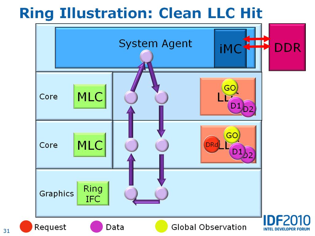
10 Cache Hierarchy Level Capacity ways Line Size (bytes) Write Update Policy Inclusive Latency (cycles) Bandwidth (Byte/cyc) L1 Data 32KB 8 64 Write-back L1 Instruction 32KB 8 64 N/A L2 (Unified) 256KB 8 64 Write-back No Varies Varies 64 Write-back Yes The is inclusive of all cache levels above it Data contained in the core caches must also reside in the Each cache line holds an indication of the cores that may have this line in their L2 and L1 caches Fetching data from when another core has the data Clean hit data is not modified in the other core 43 cycles Dirty hit data is modified in the other core 60 cycles 10 From the Optimization Manual
11 11
12 12
13 13
14 14
15 15
16 16
17 17
18 18
19 19
20 20
21 21
22 22
23 23
24 24
25 Data Prefetch to MLC and Two HW prefetchers fetch data from memory to MLC and Streamer and spatial prefetcher prefetch the data to the Typically data is brought also to the MLC Unless the MLC is heavily loaded with missing demand requests Spatial Prefetcher Strives to complete every cache line fetched to the MLC with the pair line that completes it to a 128-byte aligned chunk Streamer Prefetcher Monitors read requests from the L1 caches for ascending and descending sequences of addresses L1 D$ requests: loads, stores, and L1 D$ HW prefetcher L1 I$ code fetch requests When a forward or backward stream of requests is detected The anticipated cache lines are pre-fetched Prefetch-ed cache lines must be in the same 4K page 25 From the Optimization Manual
26 Data Prefetch to MLC and Streamer Prefetcher Enhancement The streamer may issue two prefetch requests on every MLC lookup Runs up to 20 lines ahead of the load request Adjusts dynamically to the number of outstanding requests per core Not many outstanding requests prefetch further ahead Many outstanding requests prefetch to only, and less far ahead When cache lines are far ahead Prefetch to only and not to the MLC Avoids replacement of useful cache lines in the MLC Detects and maintains up to 32 streams of data accesses For each 4K byte page, can maintain one forward and one backward stream 26 From the Optimization Manual

27 The System Agent Contains PCI Express, DMI, Memory Controller, Display Engine Contains Power Control Unit Programmable ucontroller, handles all power management and reset functions in the chip Smart integration with the ring Provides cores/graphics /Media with high BW, low latency to DRAM/IO for best performance Handles IO-to-cache coherency Separate voltage and frequency from ring/cores, Display integration for better battery life Extensive power and thermal management for PCI Express* and DDR DMI System DisplayAgent Graphics PCI Express* IMC 27 Smart I/O Integration Foil taken from IDF 2011
 Integrated display engine Handles delivering the pixels to the screen Flexible Display Interface (FDI) Connects to the PCH, where the display connectors (HDMI, DVI) are")
 e.g.")
28 System Agent Components PCIe controllers that connect to external PCIe devices Support different configurations: 16+ 4, , DMI (Direct Media Interface) controller Connects to the PCH (Platform Controller Hub) Integrated display engine Handles delivering the pixels to the screen Flexible Display Interface (FDI) Connects to the PCH, where the display connectors (HDMI, DVI) are attached DisplayPort (used for integrated display) e.g., a laptop s LCD Integrated Memory Controller (IMC) Connects to and controls the DRAM An arbiter that handles accesses from Ring and from I/O (PCIe & DMI) Routes the accesses to the right place Routes main memory traffic to the IMC Display Port FDI PCH DMI Display DMI 4 System Agent Graphics PCI Express* IMC HDMI SATA USB 16 PCIe 2ch DDR3 28
29 The Memory Controller The memory controller supports two channels of DDR Data rates of 1066MHz, 1333MHz and 1600MHz Each channel has its own resources Handles memory requests independently Contains a 32 cache-line write-data-buffer Supports 8 bytes per cycle A hash function distributes addresses are between channels Attempts to balance the load between the channels in order to achieve maximum bandwidth and minimum hotspot collisions For best performance DRAM Ctrlr CH A CH B DDR DIMM DDR DIMM Populate both channels with equal amounts of memory Preferably the exact same types of DIMMs Use highest supported speed DRAM, with the best DRAM timings 29 From the Optimization Manual
30 The Memory Controller High-performance out-of-order scheduler Attempts to maximize memory bandwidth while minimizing latency Writes to the memory controller are considered completed when they are written to the write-data-buffer The write-data-buffer is flushed out to main memory at a later time, not impacting write latency Partial writes are not handled efficiently on the memory controller May result in read-modify-write operations on the DDR channel if the partial-writes do not complete a full cache-line in time Software should avoid creating partial write transactions whenever possible E.g., buffer the partial writes into full cache line writes imc also supports high-priority isochronous requests E.g., USB isochronous, and Display isochronous requests High bandwidth of memory requests from the integrated display engine takes up some of the memory bandwidth Impacts core access latency to some degree 30 From the Optimization Manual
31 Integration: Optimization Opportunities Dynamically redistribute power between s & Graphics Tight power management control of all components, providing better granularity and deeper idle/sleep states Three separate power/frequency domains: System Agent (Fixed), s+ring, Graphics (Variable) High BW Last Level Cache, shared among s and Graphics Significant performance boost, saves memory bandwidth and power Integrated Memory Controller and PCI Express ports Tightly integrated with /Graphics/ domain Provides low latency & low power remove intermediate busses Bandwidth is balanced across the whole machine, from /Graphics all the way to Memory Controller Modular uarch for optimal cost/power/performance Derivative products done with minimal effort/time 31 Foil taken from IDF 2011
32 DRAM 32
33 Basic DRAM chip RAS# Addr Row Address Latch Row Address decoder Memory array CAS# Column Address Latch Column addr decoder Data DRAM access sequence Put Row on addr. bus and assert RAS# (Row Addr. Strobe) to latch Row Put Column on addr. bus and assert CAS# (Column Addr. Strobe) to latch Col Get data on address bus 33
34 DRAM Operation DRAM cell consists of transistor + capacitor AL Capacitor keeps the state; Transistor guards access to the state DL M C Reading cell state: raise access line AL and sense DL Capacitor charged current to flow on the data line DL Writing cell state: set DL and raise AL to charge/drain capacitor Charging and draining a capacitor is not instantaneous Leakage current drains capacitor even when transistor is closed DRAM cell periodically refreshed every 64ms 34
35 DRAM Access Sequence Timing trp Row Precharge RAS# CAS# A[0:7] Data trcd RAS/CAS delay Row i Col n Row j CL CAS latency Data n Put row address on address bus and assert RAS# Wait for RAS# to CAS# delay (trcd) between asserting RAS and CAS Put column address on address bus and assert CAS# Wait for CAS latency (CL) between time CAS# asserted and data ready Row precharge time: time to close current row, and open a new row 35
36 DRAM controller DRAM controller gets address and command Splits address to Row and Column Generates DRAM control signals at the proper timing A[20:23] address decoder Chip select Time delay gen. RAS# CAS# Select A[10:19] D[0:7] A[0:9] address mux Memory address bus DRAM R/W# DRAM data must be periodically refreshed DRAM controller performs DRAM refresh, using refresh counter 36
37 Improved DRAM Schemes Paged Mode DRAM Multiple accesses to different columns from same row Saves RAS and RAS to CAS delay RAS# CAS# A[0:7] Data Row Col n Col n+1 Col n+2 Data n D n+1 D n+2 Extended Data Output RAM (EDO RAM) A data output latch enables to parallel next column address with current column data RAS# CAS# A[0:7] Data Row Col n Col n+1 Col n+2 Data n Data n+1 Data n+2 37
38 Improved DRAM Schemes (cont) Burst DRAM Generates consecutive column address by itself RAS# CAS# A[0:7] Data Row Col n Data n Data n+1 Data n+2 38
39 Synchronous DRAM SDRAM All signals are referenced to an external clock (100MHz-200MHz) Makes timing more precise with other system devices 4 banks multiple pages open simultaneously (one per bank) Command driven functionality instead of signal driven ACTIVE: selects both the bank and the row to be activated ACTIVE to a new bank can be issued while accessing current bank READ/WRITE: select column Burst oriented read and write accesses Successive column locations accessed in the given row Burst length is programmable: 1, 2, 4, 8, and full-page May end full-page burst by BURST TERMINATE to get arbitrary burst length A user programmable Mode Register CAS latency, burst length, burst type Auto pre-charge: may close row at last read/write in burst Auto refresh: internal counters generate refresh address 39
40 SDRAM Timing clock cmd ACT NOP t RCD > 20ns RD RD+PC ACT NOP RD t RRD > 20ns ACT NOP RD NOP NOP NOP t RC >70ns BL = 1 Bank Bank 0 Bank 0Bank 0 Bank 1 Bank 1 Bank 0 Bank 0 Addr Row i Col j Col k Row m Col n Row l Col q CL=2 Data Data j Data k Data n Data q t RCD : ACTIVE to READ/WRITE gap = t RCD (MIN) / clock period t RC : successive ACTIVE to a different row in the same bank t RRD : successive ACTIVE commands to different banks 40
41 DDR-SDRAM 2n-prefetch architecture DRAM cells are clocked at the same speed as SDR SDRAM cells Internal data bus is twice the width of the external data bus Data capture occurs twice per clock cycle Lower half of the bus sampled at clock rise Upper half of the bus sampled at clock fall 0:n-1 SDRAM Array 0:2n-1 n:2n-1 0:n-1 400M xfer/sec 200MHz clock Uses 2.5V (vs. 3.3V in SDRAM) Reduced power consumption 41
42 DDR SDRAM Timing 133MHz clock cmd ACT NOP NOP RD NOP ACT NOP NOP RD NOP ACT NOP NOP t RCD >20ns t RRD >20ns t RC >70ns Bank Bank 0 Bank 0 Bank 1 Bank 1 Bank 0 Addr Row i Col j Row m Col n Row l CL=2 Data j n

43 DIMMs DIMM: Dual In-line Memory Module A small circuit board that holds memory chips 64-bit wide data path (72 bit with parity) Single sided: 9 chips, each with 8 bit data bus Dual sided: 18 chips, each with 4 bit data bus Data BW: 64 bits on each rising and falling edge of the clock Other pins Address 14, RAS, CAS, chip select 4, VDC 17, Gnd 18, clock 4, serial address 3, 43
44 DDR Standards DRAM timing, measured in I/O bus cycles, specifies 3 numbers CAS Latency RAS to CAS Delay RAS Precharge Time CAS latency (latency to get data in an open page) in nsec CAS Latency I/O bus cycle time Standard name Mem. clock (MHz) I/O bus clock (MHz) Total BW for DDR400 Cycle time (ns) Data rate (MT/s) DDR V DDQ (V) Module name 3200M Byte/sec = 64 bit 2 200MHz / 8 (bit/byte) 6400M Byte/sec for dual channel DDR SDRAM transfer rate (MB/s) PC DDR ⅓ 133⅓ ⅔ 2.5 PC ⅓ DDR ⅔ 166⅔ 6 333⅓ PC ⅔ DDR PC Timing (CL-tRCDtRP) CAS Latency (ns)

45 DDR2 DDR2 doubles the bandwidth 4n pre-fetch: internally read/write 4 the amount of data as the external bus DDR2-533 cell works at the same freq. as Memory Cell Array I/O Buffers Data Bus a DDR266 cell or a PC133 cell Prefetching increases latency Smaller page size: 1KB vs. 2KB Reduces activation power ACTIVATE command reads all bits in the page Memory Cell Array I/O Buffers Data Bus 8 banks in 1Gb densities and above Increases random accesses 1.8V (vs 2.5V) operation voltage Significantly lower power Memory Cell Array I/O Buffers Data Bus 45
46 DDR2 Standards Standard name Mem clock (MHz) Cycle time I/O Bus clock (MHz) Data rate (MT/s) Module name Peak transfer rate Timings CAS Latency DDR ns PC MB/s DDR ns PC MB/s DDR ns PC MB/s DDR ns PC MB/s DDR ns PC MB/s
47 DDR3 30% power consumption reduction compared to DDR2 1.5V supply voltage, compared to DDR2's 1.8V 90 nanometer fabrication technology Higher bandwidth 8 bit deep prefetch buffer (vs. 4 bit in DDR2 and 2 bit in DDR) Transfer data rate Effective clock rate of MHz using both rising and falling edges of a MHz I/O clock DDR2: MHz using a MHz I/O clock DDR: MHz based on a MHz I/O clock DDR3 DIMMs 240 pins, the same number as DDR2, and are the same size Electrically incompatible, and have a different key notch location 47
48 DDR3 Standards Standard Name Mem clock (MHz) I/O bus clock (MHz) I/O bus Cycle time (ns) Data rate (MT/s) Module name Peak transfer rate (MB/s) DDR PC DDR ⅓ 533⅓ ⅔ PC ⅓ DDR ⅔ 666⅔ ⅓ PC ⅔ DDR PC DDR ⅓ 933⅓ ⅔ PC ⅓ DDR ⅔ 1066⅔ ⅓ PC ⅔ Timings (CL-tRCDtRP) CAS Latency (ns)

49 DDR2 vs. DDR3 Performance The high latency of DDR3 SDRAM has negative effect on streaming operations 49 Source: xbitlabs
50 How to get the most of Memory? Each DIMM supports 4 open pages simultaneously The more open pages, the more random access It is better to have more DIMMs: n DIMMs 4n open pages Dual sided DIMMs may have separate CS of each side Support 8 open pages Dual sided DIMMs may also have a common CS 50
51 SRAM Static RAM True random access High speed, low density, high power No refresh Address not multiplexed DDR SRAM 2 READs or 2 WRITEs per clock Common or Separate I/O DDRII: 200MHz to 333MHz Operation; Density: 18/36/72Mb+ QDR SRAM Two separate DDR ports: one read and one write One DDR address bus: alternating between the read address and the write address QDRII: 250MHz to 333MHz Operation; Density: 18/36/72Mb+ 51
52 SRAM vs. DRAM Random Access: access time is the same for all locations DRAM Dynamic RAM SRAM Static RAM Refresh Refresh needed No refresh needed Address Address muxed: row+ column Address not multiplexed Access Not true Random Access True Random Access density High (1 Transistor/bit) Low (6 Transistor/bit) Power low high Speed slow fast Price/bit low high Typical usage Main memory cache 52
53 Read Only Memory (ROM) Random Access Non volatile ROM Types PROM Programmable ROM Burnt once using special equipment EPROM Erasable PROM Can be erased by exposure to UV, and then reprogrammed E 2 PROM Electrically Erasable PROM Can be erased and reprogrammed on board Write time (programming) much longer than RAM Limited number of writes (thousands) 53
Topic 21: Memory Technology
 Topic 21: Memory Technology COS / ELE 375 Computer Architecture and Organization Princeton University Fall 2015 Prof. David August 1 Old Stuff Revisited Mercury Delay Line Memory Maurice Wilkes, in 1947,
Topic 21: Memory Technology
 Topic 21: Memory Technology COS / ELE 375 Computer Architecture and Organization Princeton University Fall 2015 Prof. David August 1 Old Stuff Revisited Mercury Delay Line Memory Maurice Wilkes, in 1947,
ELEC 5200/6200 Computer Architecture and Design Spring 2017 Lecture 7: Memory Organization Part II
 ELEC 5200/6200 Computer Architecture and Design Spring 2017 Lecture 7: Organization Part II Ujjwal Guin, Assistant Professor Department of Electrical and Computer Engineering Auburn University, Auburn,
EE414 Embedded Systems Ch 5. Memory Part 2/2
 EE414 Embedded Systems Ch 5. Memory Part 2/2 Byung Kook Kim School of Electrical Engineering Korea Advanced Institute of Science and Technology Overview 6.1 introduction 6.2 Memory Write Ability and Storage
Multilevel Memories. Joel Emer Computer Science and Artificial Intelligence Laboratory Massachusetts Institute of Technology
 1 Multilevel Memories Computer Science and Artificial Intelligence Laboratory Massachusetts Institute of Technology Based on the material prepared by Krste Asanovic and Arvind CPU-Memory Bottleneck 6.823
Mainstream Computer System Components
 Mainstream Computer System Components Double Date Rate (DDR) SDRAM One channel = 8 bytes = 64 bits wide Current DDR3 SDRAM Example: PC3-12800 (DDR3-1600) 200 MHz (internal base chip clock) 8-way interleaved
ECE 485/585 Microprocessor System Design
 Microprocessor System Design Lecture 5: Zeshan Chishti DRAM Basics DRAM Evolution SDRAM-based Memory Systems Electrical and Computer Engineering Dept. Maseeh College of Engineering and Computer Science
Mainstream Computer System Components CPU Core 2 GHz GHz 4-way Superscaler (RISC or RISC-core (x86): Dynamic scheduling, Hardware speculation
: Dynamic scheduling, Hardware speculation") Mainstream Computer System Components CPU Core 2 GHz - 3.0 GHz 4-way Superscaler (RISC or RISC-core (x86): Dynamic scheduling, Hardware speculation One core or multi-core (2-4) per chip Multiple FP, integer
Mainstream Computer System Components CPU Core 2 GHz - 3.0 GHz 4-way Superscaler (RISC or RISC-core (x86): Dynamic scheduling, Hardware speculation One core or multi-core (2-4) per chip Multiple FP, integer
Embedded Systems Design: A Unified Hardware/Software Introduction. Outline. Chapter 5 Memory. Introduction. Memory: basic concepts
 Hardware/Software Introduction Chapter 5 Memory Outline Memory Write Ability and Storage Permanence Common Memory Types Composing Memory Memory Hierarchy and Cache Advanced RAM 1 2 Introduction Memory:
Embedded Systems Design: A Unified Hardware/Software Introduction. Chapter 5 Memory. Outline. Introduction
 Hardware/Software Introduction Chapter 5 Memory 1 Outline Memory Write Ability and Storage Permanence Common Memory Types Composing Memory Memory Hierarchy and Cache Advanced RAM 2 Introduction Embedded
CS650 Computer Architecture. Lecture 9 Memory Hierarchy - Main Memory
 CS65 Computer Architecture Lecture 9 Memory Hierarchy - Main Memory Andrew Sohn Computer Science Department New Jersey Institute of Technology Lecture 9: Main Memory 9-/ /6/ A. Sohn Memory Cycle Time 5
COSC 6385 Computer Architecture - Memory Hierarchies (III)
") COSC 6385 Computer Architecture - Memory Hierarchies (III) Edgar Gabriel Spring 2014 Memory Technology Performance metrics Latency problems handled through caches Bandwidth main concern for main memory
COSC 6385 Computer Architecture - Memory Hierarchies (III) Edgar Gabriel Spring 2014 Memory Technology Performance metrics Latency problems handled through caches Bandwidth main concern for main memory
EEM 486: Computer Architecture. Lecture 9. Memory
 EEM 486: Computer Architecture Lecture 9 Memory The Big Picture Designing a Multiple Clock Cycle Datapath Processor Control Memory Input Datapath Output The following slides belong to Prof. Onur Mutlu
Mark Redekopp, All rights reserved. EE 352 Unit 10. Memory System Overview SRAM vs. DRAM DMA & Endian-ness
 EE 352 Unit 10 Memory System Overview SRAM vs. DRAM DMA & Endian-ness The Memory Wall Problem: The Memory Wall Processor speeds have been increasing much faster than memory access speeds (Memory technology
CS311 Lecture 21: SRAM/DRAM/FLASH
 S 14 L21-1 2014 CS311 Lecture 21: SRAM/DRAM/FLASH DARM part based on ISCA 2002 tutorial DRAM: Architectures, Interfaces, and Systems by Bruce Jacob and David Wang Jangwoo Kim (POSTECH) Thomas Wenisch (University
UMBC. Select. Read. Write. Output/Input-output connection. 1 (Feb. 25, 2002) Four commonly used memories: Address connection ... Dynamic RAM (DRAM)
 Four commonly used memories: Address connection ... Dynamic RAM (DRAM)") Memory Types Two basic types: ROM: Read-only memory RAM: Read-Write memory Four commonly used memories: ROM Flash (EEPROM) Static RAM (SRAM) Dynamic RAM (DRAM) Generic pin configuration: Address connection
Memory Types Two basic types: ROM: Read-only memory RAM: Read-Write memory Four commonly used memories: ROM Flash (EEPROM) Static RAM (SRAM) Dynamic RAM (DRAM) Generic pin configuration: Address connection
Basics DRAM ORGANIZATION. Storage element (capacitor) Data In/Out Buffers. Word Line. Bit Line. Switching element HIGH-SPEED MEMORY SYSTEMS
 Data In/Out Buffers. Word Line. Bit Line. Switching element HIGH-SPEED MEMORY SYSTEMS") Basics DRAM ORGANIZATION DRAM Word Line Bit Line Storage element (capacitor) In/Out Buffers Decoder Sense Amps... Bit Lines... Switching element Decoder... Word Lines... Memory Array Page 1 Basics BUS
Basics DRAM ORGANIZATION DRAM Word Line Bit Line Storage element (capacitor) In/Out Buffers Decoder Sense Amps... Bit Lines... Switching element Decoder... Word Lines... Memory Array Page 1 Basics BUS
COMPUTER ARCHITECTURES
 COMPUTER ARCHITECTURES Random Access Memory Technologies Gábor Horváth BUTE Department of Networked Systems and Services ghorvath@hit.bme.hu Budapest, 2019. 02. 24. Department of Networked Systems and
CS 320 February 2, 2018 Ch 5 Memory
 CS 320 February 2, 2018 Ch 5 Memory Main memory often referred to as core by the older generation because core memory was a mainstay of computers until the advent of cheap semi-conductor memory in the
Introduction to memory system :from device to system
 Introduction to memory system :from device to system Jianhui Yue Electrical and Computer Engineering University of Maine The Position of DRAM in the Computer 2 The Complexity of Memory 3 Question Assume
JEDEC Standard No. 21 -C Page Appendix E: Specific PD s for Synchronous DRAM (SDRAM).
.") Page 4.1.2.5-1 4.1.2.5 - Appendix E: Specific PD s for Synchronous DRAM (SDRAM). 1.0 Introduction: This appendix describes the Presence Detects for Synchronous DRAM Modules with SPD revision level 2 (02h).
Page 4.1.2.5-1 4.1.2.5 - Appendix E: Specific PD s for Synchronous DRAM (SDRAM). 1.0 Introduction: This appendix describes the Presence Detects for Synchronous DRAM Modules with SPD revision level 2 (02h).
TECHNOLOGY BRIEF. Double Data Rate SDRAM: Fast Performance at an Economical Price EXECUTIVE SUMMARY C ONTENTS
 TECHNOLOGY BRIEF June 2002 Compaq Computer Corporation Prepared by ISS Technology Communications C ONTENTS Executive Summary 1 Notice 2 Introduction 3 SDRAM Operation 3 How CAS Latency Affects System Performance
INSTITUTO SUPERIOR TÉCNICO. Architectures for Embedded Computing
 UNIVERSIDADE TÉCNICA DE LISBOA INSTITUTO SUPERIOR TÉCNICO Departamento de Engenharia Informática Architectures for Embedded Computing MEIC-A, MEIC-T, MERC Lecture Slides Version 3.0 - English Lecture 16
Memory System Overview. DMA & Endian-ness. Technology. Architectural. Problem: The Memory Wall
 The Memory Wall EE 357 Unit 13 Problem: The Memory Wall Processor speeds have been increasing much faster than memory access speeds (Memory technology targets density rather than speed) Large memories
Introducing Sandy Bridge
 Introducing Sandy Bridge Bob Valentine Senior Principal Engineer 1 Sandy Bridge - Intel Next Generation Microarchitecture Sandy Bridge: Overview Integrates CPU, Graphics, MC, PCI Express* On Single Chip
Chapter 5 Internal Memory
 Chapter 5 Internal Memory Memory Type Category Erasure Write Mechanism Volatility Random-access memory (RAM) Read-write memory Electrically, byte-level Electrically Volatile Read-only memory (ROM) Read-only
Computer Systems Laboratory Sungkyunkwan University
 DRAMs Jin-Soo Kim (jinsookim@skku.edu) Computer Systems Laboratory Sungkyunkwan University http://csl.skku.edu Main Memory & Caches Use DRAMs for main memory Fixed width (e.g., 1 word) Connected by fixed-width
An introduction to SDRAM and memory controllers. 5kk73
 An introduction to SDRAM and memory controllers 5kk73 Presentation Outline (part 1) Introduction to SDRAM Basic SDRAM operation Memory efficiency SDRAM controller architecture Conclusions Followed by part
Memories: Memory Technology
 Memories: Memory Technology Z. Jerry Shi Assistant Professor of Computer Science and Engineering University of Connecticut * Slides adapted from Blumrich&Gschwind/ELE475 03, Peh/ELE475 * Memory Hierarchy
Basic Organization Memory Cell Operation. CSCI 4717 Computer Architecture. ROM Uses. Random Access Memory. Semiconductor Memory Types
 CSCI 4717/5717 Computer Architecture Topic: Internal Memory Details Reading: Stallings, Sections 5.1 & 5.3 Basic Organization Memory Cell Operation Represent two stable/semi-stable states representing
a) Memory management unit b) CPU c) PCI d) None of the mentioned
 Memory management unit b) CPU c) PCI d) None of the mentioned") 1. CPU fetches the instruction from memory according to the value of a) program counter b) status register c) instruction register d) program status word 2. Which one of the following is the address generated
1. CPU fetches the instruction from memory according to the value of a) program counter b) status register c) instruction register d) program status word 2. Which one of the following is the address generated
Computer Organization. 8th Edition. Chapter 5 Internal Memory
 William Stallings Computer Organization and Architecture 8th Edition Chapter 5 Internal Memory Semiconductor Memory Types Memory Type Category Erasure Write Mechanism Volatility Random-access memory (RAM)
Computer Architecture. Memory Hierarchy. Lynn Choi Korea University
 Computer Architecture Memory Hierarchy Lynn Choi Korea University Memory Hierarchy Motivated by Principles of Locality Speed vs. Size vs. Cost tradeoff Locality principle Temporal Locality: reference to
ECE 485/585 Midterm Exam
 ECE 485/585 Midterm Exam Time allowed: 100 minutes Total Points: 65 Points Scored: Name: Problem No. 1 (12 points) For each of the following statements, indicate whether the statement is TRUE or FALSE:
Chapter 8 Memory Basics
 Logic and Computer Design Fundamentals Chapter 8 Memory Basics Charles Kime & Thomas Kaminski 2008 Pearson Education, Inc. (Hyperlinks are active in View Show mode) Overview Memory definitions Random Access
COSC 6385 Computer Architecture - Memory Hierarchies (II)
") COSC 6385 Computer Architecture - Memory Hierarchies (II) Edgar Gabriel Spring 2018 Types of cache misses Compulsory Misses: first access to a block cannot be in the cache (cold start misses) Capacity
COSC 6385 Computer Architecture - Memory Hierarchies (II) Edgar Gabriel Spring 2018 Types of cache misses Compulsory Misses: first access to a block cannot be in the cache (cold start misses) Capacity
Memory Challenges. Issues & challenges in memory design: Cost Performance Power Scalability
 Memory Devices 1 Memory Challenges Issues & challenges in memory design: Cost Performance Power Scalability 2 Memory - Overview Definitions: RAM random access memory DRAM dynamic RAM SRAM static RAM Volatile
Internal Memory. Computer Architecture. Outline. Memory Hierarchy. Semiconductor Memory Types. Copyright 2000 N. AYDIN. All rights reserved.
 Computer Architecture Prof. Dr. Nizamettin AYDIN naydin@yildiz.edu.tr nizamettinaydin@gmail.com Internal Memory http://www.yildiz.edu.tr/~naydin 1 2 Outline Semiconductor main memory Random Access Memory
CSE 431 Computer Architecture Fall Chapter 5A: Exploiting the Memory Hierarchy, Part 1
 CSE 431 Computer Architecture Fall 2008 Chapter 5A: Exploiting the Memory Hierarchy, Part 1 Mary Jane Irwin ( www.cse.psu.edu/~mji ) [Adapted from Computer Organization and Design, 4 th Edition, Patterson
k -bit address bus n-bit data bus Control lines ( R W, MFC, etc.)
") THE MEMORY SYSTEM SOME BASIC CONCEPTS Maximum size of the Main Memory byte-addressable CPU-Main Memory Connection, Processor MAR MDR k -bit address bus n-bit data bus Memory Up to 2 k addressable locations
THE MEMORY SYSTEM SOME BASIC CONCEPTS Maximum size of the Main Memory byte-addressable CPU-Main Memory Connection, Processor MAR MDR k -bit address bus n-bit data bus Memory Up to 2 k addressable locations
15-740/ Computer Architecture Lecture 19: Main Memory. Prof. Onur Mutlu Carnegie Mellon University
 15-740/18-740 Computer Architecture Lecture 19: Main Memory Prof. Onur Mutlu Carnegie Mellon University Last Time Multi-core issues in caching OS-based cache partitioning (using page coloring) Handling
CENG4480 Lecture 09: Memory 1
 CENG4480 Lecture 09: Memory 1 Bei Yu byu@cse.cuhk.edu.hk (Latest update: November 8, 2017) Fall 2017 1 / 37 Overview Introduction Memory Principle Random Access Memory (RAM) Non-Volatile Memory Conclusion
EECS150 - Digital Design Lecture 16 - Memory
 EECS150 - Digital Design Lecture 16 - Memory October 17, 2002 John Wawrzynek Fall 2002 EECS150 - Lec16-mem1 Page 1 Memory Basics Uses: data & program storage general purpose registers buffering table lookups
Memory Hierarchy and Caches
 Memory Hierarchy and Caches COE 301 / ICS 233 Computer Organization Dr. Muhamed Mudawar College of Computer Sciences and Engineering King Fahd University of Petroleum and Minerals Presentation Outline
CS 33. Memory Hierarchy I. CS33 Intro to Computer Systems XVI 1 Copyright 2016 Thomas W. Doeppner. All rights reserved.
 CS 33 Memory Hierarchy I CS33 Intro to Computer Systems XVI 1 Copyright 2016 Thomas W. Doeppner. All rights reserved. Random-Access Memory (RAM) Key features RAM is traditionally packaged as a chip basic
The Memory Hierarchy Part I
 Chapter 6 The Memory Hierarchy Part I The slides of Part I are taken in large part from V. Heuring & H. Jordan, Computer Systems esign and Architecture 1997. 1 Outline: Memory components: RAM memory cells
ECE7995 (4) Basics of Memory Hierarchy. [Adapted from Mary Jane Irwin s slides (PSU)]
![ECE7995 (4) Basics of Memory Hierarchy. [Adapted from Mary Jane Irwin s slides (PSU)]](/thumbs/75/72807926.jpg "ECE7995 (4) Basics of Memory Hierarchy. [Adapted from Mary Jane Irwin s slides (PSU)]") ECE7995 (4) Basics of Memory Hierarchy [Adapted from Mary Jane Irwin s slides (PSU)] Major Components of a Computer Processor Devices Control Memory Input Datapath Output Performance Processor-Memory Performance
ECE7995 (4) Basics of Memory Hierarchy [Adapted from Mary Jane Irwin s slides (PSU)] Major Components of a Computer Processor Devices Control Memory Input Datapath Output Performance Processor-Memory Performance
Address connections Data connections Selection connections
 Interface (cont..) We have four common types of memory: Read only memory ( ROM ) Flash memory ( EEPROM ) Static Random access memory ( SARAM ) Dynamic Random access memory ( DRAM ). Pin connections common
Lecture 15: DRAM Main Memory Systems. Today: DRAM basics and innovations (Section 2.3)
") Lecture 15: DRAM Main Memory Systems Today: DRAM basics and innovations (Section 2.3) 1 Memory Architecture Processor Memory Controller Address/Cmd Bank Row Buffer DIMM Data DIMM: a PCB with DRAM chips
Lecture 15: DRAM Main Memory Systems Today: DRAM basics and innovations (Section 2.3) 1 Memory Architecture Processor Memory Controller Address/Cmd Bank Row Buffer DIMM Data DIMM: a PCB with DRAM chips
Memory. Lecture 22 CS301
 Memory Lecture 22 CS301 Administrative Daily Review of today s lecture w Due tomorrow (11/13) at 8am HW #8 due today at 5pm Program #2 due Friday, 11/16 at 11:59pm Test #2 Wednesday Pipelined Machine Fetch
Read and Write Cycles
 Read and Write Cycles The read cycle is shown. Figure 41.1a. The RAS and CAS signals are activated one after the other to latch the multiplexed row and column addresses respectively applied at the multiplexed
The Memory Hierarchy 1
 The Memory Hierarchy 1 What is a cache? 2 What problem do caches solve? 3 Memory CPU Abstraction: Big array of bytes Memory memory 4 Performance vs 1980 Processor vs Memory Performance Memory is very slow
DDR2 SDRAM UDIMM MT8HTF12864AZ 1GB
 Features DDR2 SDRAM UDIMM MT8HTF12864AZ 1GB For component data sheets, refer to Micron's Web site: www.micron.com Figure 1: 240-Pin UDIMM (MO-237 R/C D) Features 240-pin, unbuffered dual in-line memory
Large and Fast: Exploiting Memory Hierarchy
 CSE 431: Introduction to Operating Systems Large and Fast: Exploiting Memory Hierarchy Gojko Babić 10/5/018 Memory Hierarchy A computer system contains a hierarchy of storage devices with different costs,
Organization. 5.1 Semiconductor Main Memory. William Stallings Computer Organization and Architecture 6th Edition
 William Stallings Computer Organization and Architecture 6th Edition Chapter 5 Internal Memory 5.1 Semiconductor Main Memory 5.2 Error Correction 5.3 Advanced DRAM Organization 5.1 Semiconductor Main Memory
William Stallings Computer Organization and Architecture 6th Edition. Chapter 5 Internal Memory
 William Stallings Computer Organization and Architecture 6th Edition Chapter 5 Internal Memory Semiconductor Memory Types Semiconductor Memory RAM Misnamed as all semiconductor memory is random access
Lecture 18: DRAM Technologies
 Lecture 18: DRAM Technologies Last Time: Cache and Virtual Memory Review Today DRAM organization or, why is DRAM so slow??? Lecture 18 1 Main Memory = DRAM Lecture 18 2 Basic DRAM Architecture Lecture
Introduction read-only memory random access memory
 Memory Interface Introduction Simple or complex, every microprocessorbased system has a memory system. Almost all systems contain two main types of memory: read-only memory (ROM) and random access memory
Mainstream Computer System Components
 Mainstream Computer System Components Double Date Rate (DDR) SDRAM One channel = 8 bytes = 64 bits wide Current DDR3 SDRAM Example: PC3-2800 (DDR3-600) 200 MHz (internal base chip clock) 8-way interleaved
EECS150 - Digital Design Lecture 16 Memory 1
 EECS150 - Digital Design Lecture 16 Memory 1 March 13, 2003 John Wawrzynek Spring 2003 EECS150 - Lec16-mem1 Page 1 Memory Basics Uses: Whenever a large collection of state elements is required. data &
Chapter 5B. Large and Fast: Exploiting Memory Hierarchy
 Chapter 5B Large and Fast: Exploiting Memory Hierarchy One Transistor Dynamic RAM 1-T DRAM Cell word access transistor V REF TiN top electrode (V REF ) Ta 2 O 5 dielectric bit Storage capacitor (FET gate,
Memory latency: Affects cache miss penalty. Measured by:
 Main Memory Main memory generally utilizes Dynamic RAM (DRAM), which use a single transistor to store a bit, but require a periodic data refresh by reading every row. Static RAM may be used for main memory
William Stallings Computer Organization and Architecture 8th Edition. Chapter 5 Internal Memory
 William Stallings Computer Organization and Architecture 8th Edition Chapter 5 Internal Memory Semiconductor Memory The basic element of a semiconductor memory is the memory cell. Although a variety of
The Memory Component
 The Computer Memory Chapter 6 forms the first of a two chapter sequence on computer memory. Topics for this chapter include. 1. A functional description of primary computer memory, sometimes called by
LECTURE 5: MEMORY HIERARCHY DESIGN
 LECTURE 5: MEMORY HIERARCHY DESIGN Abridged version of Hennessy & Patterson (2012):Ch.2 Introduction Programmers want unlimited amounts of memory with low latency Fast memory technology is more expensive
Spring 2018 :: CSE 502. Main Memory & DRAM. Nima Honarmand
 Main Memory & DRAM Nima Honarmand Main Memory Big Picture 1) Last-level cache sends its memory requests to a Memory Controller Over a system bus of other types of interconnect 2) Memory controller translates
The DRAM Cell. EEC 581 Computer Architecture. Memory Hierarchy Design (III) 1T1C DRAM cell
 1T1C DRAM cell") EEC 581 Computer Architecture Memory Hierarchy Design (III) Department of Electrical Engineering and Computer Science Cleveland State University The DRAM Cell Word Line (Control) Bit Line (Information)
EEC 581 Computer Architecture Memory Hierarchy Design (III) Department of Electrical Engineering and Computer Science Cleveland State University The DRAM Cell Word Line (Control) Bit Line (Information)
CPE300: Digital System Architecture and Design
 CPE300: Digital System Architecture and Design Fall 2011 MW 17:30-18:45 CBC C316 Cache 11232011 http://www.egr.unlv.edu/~b1morris/cpe300/ 2 Outline Review Memory Components/Boards Two-Level Memory Hierarchy
DDR SDRAM UDIMM. Draft 9/ 9/ MT18VDDT6472A 512MB 1 MT18VDDT12872A 1GB For component data sheets, refer to Micron s Web site:
 DDR SDRAM UDIMM MT18VDDT6472A 512MB 1 MT18VDDT12872A 1GB For component data sheets, refer to Micron s Web site: www.micron.com 512MB, 1GB (x72, ECC, DR) 184-Pin DDR SDRAM UDIMM Features Features 184-pin,
CS 152 Computer Architecture and Engineering. Lecture 7 - Memory Hierarchy-II
 CS 152 Computer Architecture and Engineering Lecture 7 - Memory Hierarchy-II Krste Asanovic Electrical Engineering and Computer Sciences University of California at Berkeley http://www.eecs.berkeley.edu/~krste
Main Memory. EECC551 - Shaaban. Memory latency: Affects cache miss penalty. Measured by:
 Main Memory Main memory generally utilizes Dynamic RAM (DRAM), which use a single transistor to store a bit, but require a periodic data refresh by reading every row (~every 8 msec). Static RAM may be
Memory latency: Affects cache miss penalty. Measured by:
 Main Memory Main memory generally utilizes Dynamic RAM (DRAM), which use a single transistor to store a bit, but require a periodic data refresh by reading every row. Static RAM may be used for main memory
CENG3420 Lecture 08: Memory Organization
 CENG3420 Lecture 08: Memory Organization Bei Yu byu@cse.cuhk.edu.hk (Latest update: February 22, 2018) Spring 2018 1 / 48 Overview Introduction Random Access Memory (RAM) Interleaving Secondary Memory
Memory Device Evolution
 Memory Device Evolution Cassino May 2008 Maurizio Di Zenzo Applications Lab Mgr Agenda Random access memories A quick comparison of technologies Details of external memory technologies Solutions for low
MEMORY SYSTEM MEMORY TECHNOLOGY SUMMARY DESIGNING MEMORY SYSTEM. The goal in designing any memory system is to provide
 SUMMARY MEMORY SYSTEM ORGANIZATION Memory technology Hierarchical memory systems Characteristics of the storage-device Main memory organization SRAM DRAM Cache memory COMPUTER ARCHITECTURE 2 MEMORY TECHNOLOGY
Organization Row Address Column Address Bank Address Auto Precharge 128Mx8 (1GB) based module A0-A13 A0-A9 BA0-BA2 A10
 based module A0-A13 A0-A9 BA0-BA2 A10") GENERAL DESCRIPTION The Gigaram is ECC Registered Dual-Die DIMM with 1.25inch (30.00mm) height based on DDR2 technology. DIMMs are available as ECC modules in 256Mx72 (2GByte) organization and density,
GENERAL DESCRIPTION The Gigaram is ECC Registered Dual-Die DIMM with 1.25inch (30.00mm) height based on DDR2 technology. DIMMs are available as ECC modules in 256Mx72 (2GByte) organization and density,
EECS150 - Digital Design Lecture 17 Memory 2
 EECS150 - Digital Design Lecture 17 Memory 2 October 22, 2002 John Wawrzynek Fall 2002 EECS150 Lec17-mem2 Page 1 SDRAM Recap General Characteristics Optimized for high density and therefore low cost/bit
Memory systems. Memory technology. Memory technology Memory hierarchy Virtual memory
 Memory systems Memory technology Memory hierarchy Virtual memory Memory technology DRAM Dynamic Random Access Memory bits are represented by an electric charge in a small capacitor charge leaks away, need
Memory technology and optimizations ( 2.3) Main Memory
 Main Memory") Memory technology and optimizations ( 2.3) 47 Main Memory Performance of Main Memory: Latency: affects Cache Miss Penalty» Access Time: time between request and word arrival» Cycle Time: minimum time between
Memory technology and optimizations ( 2.3) 47 Main Memory Performance of Main Memory: Latency: affects Cache Miss Penalty» Access Time: time between request and word arrival» Cycle Time: minimum time between
Memory Systems for Embedded Applications. Chapter 4 (Sections )
") Memory Systems for Embedded Applications Chapter 4 (Sections 4.1-4.4) 1 Platform components CPUs. Interconnect buses. Memory. Input/output devices. Implementations: System-on-Chip (SoC) vs. Multi-Chip
Memory Systems for Embedded Applications Chapter 4 (Sections 4.1-4.4) 1 Platform components CPUs. Interconnect buses. Memory. Input/output devices. Implementations: System-on-Chip (SoC) vs. Multi-Chip
ECSE-2610 Computer Components & Operations (COCO)
") ECSE-2610 Computer Components & Operations (COCO) Part 18: Random Access Memory 1 Read-Only Memories 2 Why ROM? Program storage Boot ROM for personal computers Complete application storage for embedded
ECSE-2610 Computer Components & Operations (COCO) Part 18: Random Access Memory 1 Read-Only Memories 2 Why ROM? Program storage Boot ROM for personal computers Complete application storage for embedded
Introduction to cache memories
 Course on: Advanced Computer Architectures Introduction to cache memories Prof. Cristina Silvano Politecnico di Milano email: cristina.silvano@polimi.it 1 Summary Summary Main goal Spatial and temporal
Computer Memory Basic Concepts. Lecture for CPSC 5155 Edward Bosworth, Ph.D. Computer Science Department Columbus State University
 Computer Memory Basic Concepts Lecture for CPSC 5155 Edward Bosworth, Ph.D. Computer Science Department Columbus State University The Memory Component The memory stores the instructions and data for an
2GB DDR3 SDRAM SODIMM with SPD
 2GB DDR3 SDRAM SODIMM with SPD Ordering Information Part Number Bandwidth Speed Grade Max Frequency CAS Latency Density Organization Component Composition Number of Rank 78.A2GC6.AF1 10.6GB/sec 1333Mbps
,e-pg PATHSHALA- Computer Science Computer Architecture Module 25 Memory Hierarchy Design - Basics
 ,e-pg PATHSHALA- Computer Science Computer Architecture Module 25 Memory Hierarchy Design - Basics The objectives of this module are to discuss about the need for a hierarchical memory system and also
Design and Implementation of High Performance DDR3 SDRAM controller
 Design and Implementation of High Performance DDR3 SDRAM controller Mrs. Komala M 1 Suvarna D 2 Dr K. R. Nataraj 3 Research Scholar PG Student(M.Tech) HOD, Dept. of ECE Jain University, Bangalore SJBIT,Bangalore
LE4ASS21PEH 16GB Unbuffered 2048Mx64 DDR4 SO-DIMM 1.2V Up to PC CL
 LE4ASS21PEH 16GB Unbuffered 2048Mx64 DDR4 SO-DIMM 1.2V Up to PC4-2133 CL 15-15-15 General Description This Legacy device is a JEDEC standard unbuffered SO-DIMM module, based on CMOS DDR4 SDRAM technology,
The University of Adelaide, School of Computer Science 13 September 2018
 Computer Architecture A Quantitative Approach, Sixth Edition Chapter 2 Memory Hierarchy Design 1 Programmers want unlimited amounts of memory with low latency Fast memory technology is more expensive per
DDR SDRAM UDIMM MT8VDDT3264A 256MB MT8VDDT6464A 512MB For component data sheets, refer to Micron s Web site:
 DDR SDRAM UDIMM MT8VDDT3264A 256MB MT8VDDT6464A 512MB For component data sheets, refer to Micron s Web site: www.micron.com 256MB, 512MB (x64, SR) 184-Pin DDR SDRAM UDIMM Features Features 184-pin, unbuffered
Options. Data Rate (MT/s) CL = 3 CL = 2.5 CL = 2-40B PC PC PC
 CL = 3 CL = 2.5 CL = 2-40B PC PC PC") DDR SDRAM UDIMM MT16VDDF6464A 512MB 1 MT16VDDF12864A 1GB 1 For component data sheets, refer to Micron s Web site: www.micron.com 512MB, 1GB (x64, DR) 184-Pin DDR SDRAM UDIMM Features Features 184-pin,
DDR SDRAM UDIMM MT16VDDF6464A 512MB 1 MT16VDDF12864A 1GB 1 For component data sheets, refer to Micron s Web site: www.micron.com 512MB, 1GB (x64, DR) 184-Pin DDR SDRAM UDIMM Features Features 184-pin,
Computer Memory. Textbook: Chapter 1
 Computer Memory Textbook: Chapter 1 ARM Cortex-M4 User Guide (Section 2.2 Memory Model) STM32F4xx Technical Reference Manual: Chapter 2 Memory and Bus Architecture Chapter 3 Flash Memory Chapter 36 Flexible
DDR SDRAM UDIMM MT16VDDT6464A 512MB MT16VDDT12864A 1GB MT16VDDT25664A 2GB
 DDR SDRAM UDIMM MT16VDDT6464A 512MB MT16VDDT12864A 1GB MT16VDDT25664A 2GB For component data sheets, refer to Micron s Web site: www.micron.com 512MB, 1GB, 2GB (x64, DR) 184-Pin DDR SDRAM UDIMM Features
Computer Architecture A Quantitative Approach, Fifth Edition. Chapter 2. Memory Hierarchy Design. Copyright 2012, Elsevier Inc. All rights reserved.
 Computer Architecture A Quantitative Approach, Fifth Edition Chapter 2 Memory Hierarchy Design 1 Introduction Programmers want unlimited amounts of memory with low latency Fast memory technology is more
Design with Microprocessors
 Design with Microprocessors Lecture 12 DRAM, DMA Year 3 CS Academic year 2017/2018 1 st semester Lecturer: Radu Danescu The DRAM memory cell X- voltage on Cs; Cs ~ 25fF Write: Cs is charged or discharged
1. The values of t RCD and t RP for -335 modules show 18ns to align with industry specifications; actual DDR SDRAM device specifications are 15ns.
 UDIMM MT4VDDT1664A 128MB MT4VDDT3264A 256MB For component data sheets, refer to Micron s Web site: www.micron.com 128MB, 256MB (x64, SR) 184-Pin UDIMM Features Features 184-pin, unbuffered dual in-line
Overview. Memory Classification Read-Only Memory (ROM) Random Access Memory (RAM) Functional Behavior of RAM. Implementing Static RAM
 Random Access Memory (RAM) Functional Behavior of RAM. Implementing Static RAM") Memories Overview Memory Classification Read-Only Memory (ROM) Types of ROM PROM, EPROM, E 2 PROM Flash ROMs (Compact Flash, Secure Digital, Memory Stick) Random Access Memory (RAM) Types of RAM Static
Memories Overview Memory Classification Read-Only Memory (ROM) Types of ROM PROM, EPROM, E 2 PROM Flash ROMs (Compact Flash, Secure Digital, Memory Stick) Random Access Memory (RAM) Types of RAM Static
CS 33. Architecture and Optimization (3) CS33 Intro to Computer Systems XVI 1 Copyright 2018 Thomas W. Doeppner. All rights reserved.
 CS33 Intro to Computer Systems XVI 1 Copyright 2018 Thomas W. Doeppner. All rights reserved.") CS 33 Architecture and Optimization (3) CS33 Intro to Computer Systems XVI 1 Copyright 2018 Thomas W. Doeppner. All rights reserved. Hyper Threading Instruction Control Instruction Control Retirement Unit
CS 33 Architecture and Optimization (3) CS33 Intro to Computer Systems XVI 1 Copyright 2018 Thomas W. Doeppner. All rights reserved. Hyper Threading Instruction Control Instruction Control Retirement Unit
4GB Unbuffered VLP DDR3 SDRAM DIMM with SPD
 4GB Unbuffered VLP DDR3 SDRAM DIMM with SPD Ordering Information Part Number Bandwidth Speed Grade Max Frequency CAS Latency Density Organization Component Composition 78.B1GE3.AFF0C 12.8GB/sec 1600Mbps
A Low Power DDR SDRAM Controller Design P.Anup, R.Ramana Reddy
 A Low Power DDR SDRAM Controller Design P.Anup, R.Ramana Reddy Abstract This paper work leads to a working implementation of a Low Power DDR SDRAM Controller that is meant to be used as a reference for
Chapter 5. Internal Memory. Yonsei University
 Chapter 5 Internal Memory Contents Main Memory Error Correction Advanced DRAM Organization 5-2 Memory Types Memory Type Category Erasure Write Mechanism Volatility Random-access memory(ram) Read-write