Memory Challenges. Issues & challenges in memory design: Cost Performance Power Scalability
|
|
|
- Linette Murphy
- 5 years ago
- Views:
Transcription
1 Memory Devices 1
2 Memory Challenges Issues & challenges in memory design: Cost Performance Power Scalability 2
3 Memory - Overview Definitions: RAM random access memory DRAM dynamic RAM SRAM static RAM Volatile memory the RAMs lose data when power is removed Nonvolatile memory retain data when the power is off ISP in-system programmable 3
4 Functionality Static RAM (SRAM) A word, once written at a location, remains stored as long as power is on, unless the same location is written to again Basic structure and operations Read operation: while the address is asserted, and CS (chip select) and OE (output enable) are asserted, DOUT are read out Write operation: while the address and CS/WE are asserted (write enable), a data word placed on DIN (data input) is written into the memory 4
5 SRAM Timing (1) Read operation timing parameters t AA access time from address t ACS access time from chip select t OE output-enable time t OZ output-disable time t OH output-hold time 5
6 SRAM Timing (2) Write operation timing parameters t AS address setup time before write t AH address hold time after write t CSW chip-select setup time before end of write t WP write pulse width t DS data setup time before end of write t DH data hold time after end of write 6
7 Synchronous SRAM Synchronous Clocked interfaces for control, address and data Internal structure Edge-triggered registers AREG for address CREG for control INREG for input data OUTREG for output data 7
8 Functionality Operation of One Bit Cell Dynamic RAM (DRAM) Periodically refresh the stored data by reading it and then writing ing it back, otherwise the data disappears Write operation: Set word line HIGH; To store 1, set bit line HIGH, charging the capacitor; To store 0, set LOW on the bit line, discharging the capacitor Read operation: Set word line HIGH; Bit line is precharged halfway between HIGH and LOW; The capacitor voltage pulls the bit line slightly higher or lower; A sense amplifier detects this small change and recovers 1 or 0. 1-bit storage cell 8
9 DRAM Basic Structure Basic one transistor storage cell together with cross-coupled coupled latch sense amplifier 9
10 DRAM Refreshing Reading destroys the original voltage on the capacitor, so that the recovered data must be written back into the cell after reading DRAM uses refresh cycles to periodically update memory cells Sequentially reading the degraded contents of each cell into a D latch and writing it back to a solid LOW or HIGH Voltage stored in a DRAM cell after writing and refresh operations 10
11 DRAM Internal Structure The physical array is square, for example, 64K X 1 containing 256 X 256 bits Only 8 multiplexed address inputs, saving pins which are important for compact design of memory system A complete 16-bit address is presented in two steps controlled by two signals: RAS_L row address strobe CAS_L column address strobe 11 Internal structure of a 64K X 1 DRAM
12 Read operation DRAM Timing (1) Read a selected row into the row latch column address is applied and stored in the column address register on the falling edge of CAS_L The column address is used to select one bit of the read row As long as CAS_L is asserted, a three-state pin, DOUT, is output-enabled As soon as RAS_L is negated, the entire row is written back 12
13 DRAM Timing (2) Write operation WE_L(write enable) must be asserted before CAS_L is asserted to select a write cycle and to disable DOUT for the rest of the cycle once the selected row is read into the row latch, WE_L also forces the input bit on DIN to be merged into the row latch, in the bit position selected by column address When the row is subsequently written back into the array on the rising edge of RAS_L, it contains a new value in the selected column 13
14 DRAM Other Timing Types CAS-before-RAS refresh cycle Read-modify-write cycle Page-mode read cycle Page-mode write cycle 14
15 Synchronous DRAM (SDRAM) Why synchronous The conventional RAS/CAS edge-based DRAM can not run fast and need to meet timing margins when interfacing with the rest of the system External signals CLK: samples an SDRAM s s control signal and address inputs on the rising edge of a common clock signal CKE: clock enable signal so that inputs are ignored if CKE is not asserted RAS_L, CAS_L and WE_L: command words High-order address bits: interpreted as a bank select to indicate which bank a command word applies to 15
16 DRAM Other Types FPM (Fast Page Mode) DRAM EDO DRAM (Extended Data Out DRAM) RLDRAM (Reduced Latency DRAM) 16
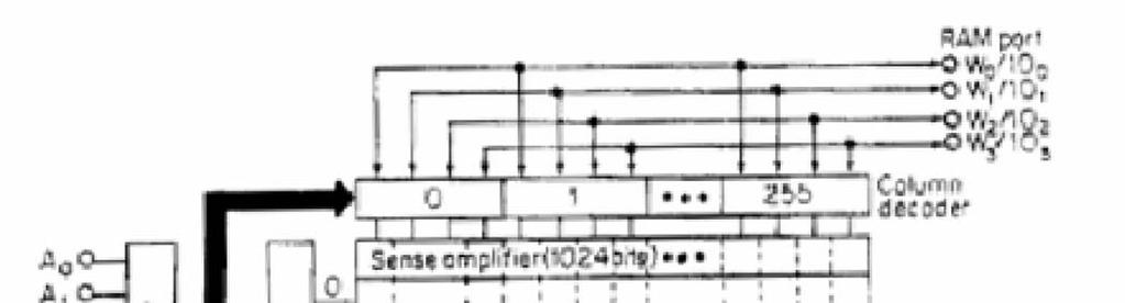
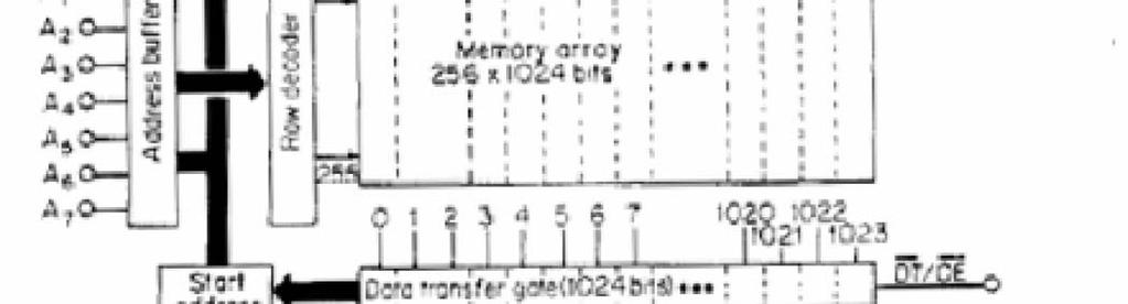
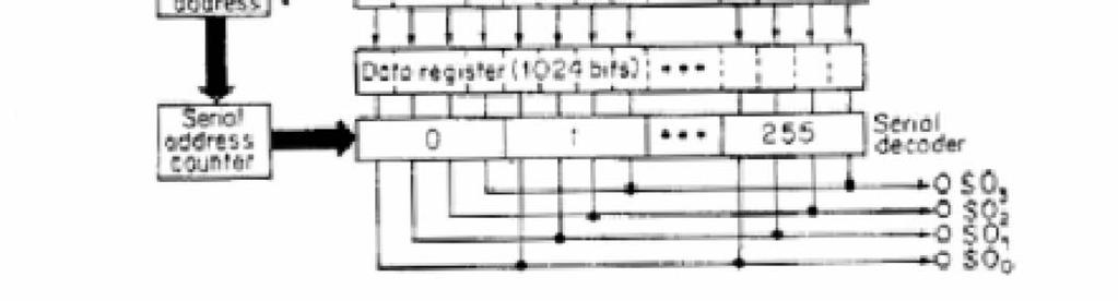
17 Special Application Memory (1) Video RAM (VRAM) 17
18 Special Application Memory (2) Dual-Port RAM 18
19 Read-Only Memory (ROM) Mask ROM Programmable ROM (PROM) Erasable programmable ROM (EPROM) Electrically erasable programmable ROM (EEPROM) 19
20 Flash Memory Electrically erasable, programmable, and nonvolatile Write or erase data in blocks Much faster than EEPROM 20
21 Banks and Ranks Bank: the entire memory array of individual bit cells is divided into sub-arrays called banks Banks allow a device s s memory core to be repaired of manufacturing defects by mapping in redundant core components Banks increase performance of a single device by facilitating concurrent operations Rank: A term that is descriptive of a multichip memory module A rank is a group of memory chips on a memory module that get selected simultaneously and that together form a data word width identical to the width of the memory data bus 21
22 Definition: DDR (Double Data Rate) SDRAM DDR SDRAM (double data rate synchronous DRAM) is a type of DRAM that realize twice the data transfer rate of conventional SDRAM DDR SDRAM is synchronous DRAM that realizes high- speed data transfer while adhering to the specifications of SDRAM as much as possible Differences from SDRAM Functions and specifications Commands Operation timing 22
23 Difference between DDR and SDR SDRAM - Functions and specifications * Conventional SDRAM is referred to as SDR SDRAM (single data rate synchronous DRAM) 23
24 Difference between DDR and SDR SDRAM - Functions and specifications (cont( cont) Twice data transfer rate is achieved by using 2-bit 2 prefetch architecture, with read cycle as example here 24
25 Difference between DDR and SDR SDRAM - Functions and specifications (cont( cont) Explanation of read cycle 2n bits of data are transferred from the memory cell array to the I/O buffer every clock Data transferred to the I/O buffer is output n bits at a time every half clock As the internal bus width is twice the external bus width, a data output rate twice the data rate of the internal bus is achieved 25
26 Use of DLL in DDR SDRAM DLL (delay locked loop) circuit is used in DDR SDRAM A fast access time and high operation frequencies are realized by controlling and adjusting the time lag between external clock and internal clock 26
27 Operation Timing of DDR SDRAM Read cycle timing Write cycle timing 27
28 Operation Timing of DDR SDRAM (cont( cont) Explanation of operation timing - Command signal READ/WRIT at rising edge of clock (CK) - Data input/output timing employs differential clock (CK and /CK) - Data strobe signal (DQS) is adopted to achieve high-speed data transfer. DQS is output from the device and received by the receiver, which adjusts the data (DQ) capture timing using DQS - Data is edge-aligned to DQS for read data and center-aligned for write data. This means that when controller receives read data from DDR SDRAM, it will internally delay the received strobe to the center of the received data window 28
29 FCRAM (Fast Cycle RAM) New technology developed by the Fujitsu Corporation Change the DRAM core itself. The process included pipeline operation and core segmentation with the added benefit of power reduction Address input can be made in parallel with command input. With this pipelining scheme, it s s possible to start a command operation while a data read or write operation is still in process, resulting in an improvement of the cycle time 29
30 FCRAM (cont( cont) FCRAM cores are used in three types of FCRAM memory devices: Network FCRAM FCRAM with a DDR synchronous interface used in networking, graphics, and multimedia Mobile FCRAM FCRAM with an asynchronous SRAM interface for mobile phone applications Consumer FCRAM FCRAM with a synchronous SDR SDRAM interface for use in consumer applications such as cameras, battery-driven devices, and car navigation systems 30
31 FCRAM (cont( cont) Representative values of Network, Mobile, and Consumer FCRAM 31
32 FCRAM (cont( cont) Representative values of Network, Mobile, and Consumer FCRAM (cont) 32
33 SigmaRAM Definition and features: Definition and features: A family of SRAM products jointly defined by the SigmaRAM Consortium The SigmaRAM family consists of devices featuring common I/O buses Designed especially for networking applications, the family of devices features higher speed, new packaging, an improved clocking scheme, multimode operation, and low power SigmaRAM packaging is also designed for networking 33
34 RLDRAM (Reduced Latency DRAM) Definition and features: Definition and features: Codeveloped by Micron Technology and Infineon Technologies Its defining characteristics include High density High bandwidth Reduced cycle time SRAM-like access Ideal for switch and router applications, and also for other high-bandwidth, high-speed, and latency-sensitive applications 34
35 DDR SRAM (Double( Data Rate SRAM DDR, DDRII SRAM) DSRAM has evolved over time to exhibit higher clock frequencies, shorter cycle times, and higher densities 35
36 DDR SRAM (cont( cont) Feature comparison of DDR and DDRII SRAM 36
37 Flash Memory Electrically erasable, programmable and nonvolatile Data to be written or erased in blocks other than one byte at a time like EEPROM Applications: digital cellular phones, digital cameras, LAN switches, etc; also can be used as embedded memory or in packaged, removable memory cards, and is also a variable choice for solid data storage replacing magnetic tapes and low-density hard disk drives Flash densities: range from 1 Mb to 8Gb Flash access times: most applications use flash devices with random access times of ns 37
38 Flash Memory (cont( cont) Flash memory performance increases with greater complexity Performance here refers to the speed with which several read and write operations can be made The major benefit of operating in page mode versus the standard mode is the greater speed A page is a small group of memory words that are accessed, internal to the memory, in parallel rather than one at a time 38
39 Flash Memory (cont( cont) Example timing diagram for page-mode read (byte mode) - The page size of the example device is 8 words (16 bytes). The higher address bits A3-A19 select the page, and the LSB bits A0-A2 (in word mode) and A-1 to A2 (in byte mode) select the specific word/byte within page - The first read has an access time t ACC, which is typical of a standard flash device, however a subsequent page read access to a location anywhere within the same page is much faster, and this access time is denoted as t PACC - Fast page-mode accesses are obtained by keeping A3-A19 constant and changing A0-A2 to select the specific word, or changing A-1 to A2 to select the specific byte within that page 39
40 Flash Cards Flash memory chips are conveniently packaged as flash cards and come in several formats, including the full-size PC Card (ATA PC Card) and the smaller CompactFlash, SmartMedia, and similar formats 40
41 FeRAM (Ferroelectric RAM) and MRAM (Magnetoresistive RAM) Features and performance: Features and performance: The next-generation nonvolatile memory for imminent commercialization MRAM uses magnetic, thin film elements on a silicon substrate. Data is written and read by pulsing wires that are perpendicular to each other with one set above and the other below the magnetic 7 MRAM can reach theoretical write times down to 2.3 ns, 1,000 times faster than the fastest nonvolatile flash and 20 times faster than FeRAM MRAM access times are as fast as 3 ns, or 20 times faster than DRAM, consuming less than 1/100 the energy of DRAM MRAM s resistance to radiation makes it to be considered a prime replacement for SRAM, which suffers more and more from densityinduced, soft-error rates as it scales below 0.1um 41
42 Quad Data Rate (QDR) SRAM Address Rate: 2-word 2 burst QDR SRAM - Sustain both a 2-word 2 read and a 2-word 2 write each clock cycle - The SRAM utilizes first ½ clock cycle to perform a read nad the other ½ clock cycle to perform a write operation. - The address bus is shared for the read and write data ports, necessitating double address rate (DAR) operation - The clock to register, the read address and the clock to register and the write address are 180 out of phase 42
43 QDR SRAM (cont( cont) Address Rate: 4-word 4 burst QDR SRAM - Sustain both a 4-word 4 read and a 4-word 4 write every clock cycle - The SRAM utilizes first clock cycle to perform a read nad the other clock cycle to perform a write operation. - The 4-word 4 read data is output during two cycles (4-word burst) - Double data address rate (DAR) is needed - The rising edge of the positive signal of differential master clock signal is used to register the read address. The next rising edge is used to latch the write address. 43
44 QDR SRAM (cont( cont) Write data placement One approach to using separate input and output clocks of the QDR SRAMs QDR SRAMs have both input and output clocks 44
45 QDR SRAM (cont( cont) Timing diagram for QDR Window of valid data = (t KHKH t CO ) + t DOH - t KHKH : rising edge of clock to rising edge of clock 180 out of phase - t CO : clock to data output time - t DOH : the data hold time 45


46 Direct Rambus DRAM (DRDRAM) PC memory system architecture for RDRAM Electrical topology comparison The RDRAM memory interface features: - The highest bandwidth per pin - Supported DRAM densities from Mb with a roadmap to support up to 1 Gb - Speed bins of 800, 1,066, 1,200, 1,333 Mbps with a roadmap to support up to 1,600 Mbps - Memory configurable into single or dual RIMM modules supporting bandwidths from 1.6 GB/s to 5.3 GB/s with a roadmap to support up to 12.8 GB/set quad-channel module 46


47 DRDRAM (cont( cont) Comparison of consumer HDTV decoder designs showing reduced chip count with the use of RDRAM Memory system architecture comparison 47
48 DRDRAM (cont( cont) Overview of a 16-bit wide-channel system 48
49 DRDRAM (cont( cont) Overview of a Rambus 16-bit system motherboard 49
50 Clock generator architecture DRDRAM (cont( cont) Channel termination Clock output drivers with example component values shown for a channel impedance of 28 Ohm 50
ECE 485/585 Microprocessor System Design
 Microprocessor System Design Lecture 5: Zeshan Chishti DRAM Basics DRAM Evolution SDRAM-based Memory Systems Electrical and Computer Engineering Dept. Maseeh College of Engineering and Computer Science
Internal Memory. Computer Architecture. Outline. Memory Hierarchy. Semiconductor Memory Types. Copyright 2000 N. AYDIN. All rights reserved.
 Computer Architecture Prof. Dr. Nizamettin AYDIN naydin@yildiz.edu.tr nizamettinaydin@gmail.com Internal Memory http://www.yildiz.edu.tr/~naydin 1 2 Outline Semiconductor main memory Random Access Memory
Computer Organization. 8th Edition. Chapter 5 Internal Memory
 William Stallings Computer Organization and Architecture 8th Edition Chapter 5 Internal Memory Semiconductor Memory Types Memory Type Category Erasure Write Mechanism Volatility Random-access memory (RAM)
Memories: Memory Technology
 Memories: Memory Technology Z. Jerry Shi Assistant Professor of Computer Science and Engineering University of Connecticut * Slides adapted from Blumrich&Gschwind/ELE475 03, Peh/ELE475 * Memory Hierarchy
William Stallings Computer Organization and Architecture 6th Edition. Chapter 5 Internal Memory
 William Stallings Computer Organization and Architecture 6th Edition Chapter 5 Internal Memory Semiconductor Memory Types Semiconductor Memory RAM Misnamed as all semiconductor memory is random access
Basics DRAM ORGANIZATION. Storage element (capacitor) Data In/Out Buffers. Word Line. Bit Line. Switching element HIGH-SPEED MEMORY SYSTEMS
 Data In/Out Buffers. Word Line. Bit Line. Switching element HIGH-SPEED MEMORY SYSTEMS") Basics DRAM ORGANIZATION DRAM Word Line Bit Line Storage element (capacitor) In/Out Buffers Decoder Sense Amps... Bit Lines... Switching element Decoder... Word Lines... Memory Array Page 1 Basics BUS
Basics DRAM ORGANIZATION DRAM Word Line Bit Line Storage element (capacitor) In/Out Buffers Decoder Sense Amps... Bit Lines... Switching element Decoder... Word Lines... Memory Array Page 1 Basics BUS
Real Time Embedded Systems
 Real Time Embedded Systems " Memories " rene.beuchat@epfl.ch LAP/ISIM/IC/EPFL Chargé de cours LSN/hepia Prof. HES 1998-2008 2 General classification of electronic memories Non-volatile Memories ROM PROM
Basic Organization Memory Cell Operation. CSCI 4717 Computer Architecture. ROM Uses. Random Access Memory. Semiconductor Memory Types
 CSCI 4717/5717 Computer Architecture Topic: Internal Memory Details Reading: Stallings, Sections 5.1 & 5.3 Basic Organization Memory Cell Operation Represent two stable/semi-stable states representing
Chapter 5 Internal Memory
 Chapter 5 Internal Memory Memory Type Category Erasure Write Mechanism Volatility Random-access memory (RAM) Read-write memory Electrically, byte-level Electrically Volatile Read-only memory (ROM) Read-only
Organization. 5.1 Semiconductor Main Memory. William Stallings Computer Organization and Architecture 6th Edition
 William Stallings Computer Organization and Architecture 6th Edition Chapter 5 Internal Memory 5.1 Semiconductor Main Memory 5.2 Error Correction 5.3 Advanced DRAM Organization 5.1 Semiconductor Main Memory
UNIT V (PROGRAMMABLE LOGIC DEVICES)
") UNIT V (PROGRAMMABLE LOGIC DEVICES) Introduction There are two types of memories that are used in digital systems: Random-access memory(ram): perform both the write and read operations. Read-only memory(rom):
UNIT V (PROGRAMMABLE LOGIC DEVICES) Introduction There are two types of memories that are used in digital systems: Random-access memory(ram): perform both the write and read operations. Read-only memory(rom):
Introduction read-only memory random access memory
 Memory Interface Introduction Simple or complex, every microprocessorbased system has a memory system. Almost all systems contain two main types of memory: read-only memory (ROM) and random access memory
ECSE-2610 Computer Components & Operations (COCO)
") ECSE-2610 Computer Components & Operations (COCO) Part 18: Random Access Memory 1 Read-Only Memories 2 Why ROM? Program storage Boot ROM for personal computers Complete application storage for embedded
ECSE-2610 Computer Components & Operations (COCO) Part 18: Random Access Memory 1 Read-Only Memories 2 Why ROM? Program storage Boot ROM for personal computers Complete application storage for embedded
(Advanced) Computer Organization & Architechture. Prof. Dr. Hasan Hüseyin BALIK (5 th Week)
 Computer Organization & Architechture. Prof. Dr. Hasan Hüseyin BALIK (5 th Week)") + (Advanced) Computer Organization & Architechture Prof. Dr. Hasan Hüseyin BALIK (5 th Week) + Outline 2. The computer system 2.1 A Top-Level View of Computer Function and Interconnection 2.2 Cache Memory
+ (Advanced) Computer Organization & Architechture Prof. Dr. Hasan Hüseyin BALIK (5 th Week) + Outline 2. The computer system 2.1 A Top-Level View of Computer Function and Interconnection 2.2 Cache Memory
Computer Systems Laboratory Sungkyunkwan University
 DRAMs Jin-Soo Kim (jinsookim@skku.edu) Computer Systems Laboratory Sungkyunkwan University http://csl.skku.edu Main Memory & Caches Use DRAMs for main memory Fixed width (e.g., 1 word) Connected by fixed-width
Chapter 8 Memory Basics
 Logic and Computer Design Fundamentals Chapter 8 Memory Basics Charles Kime & Thomas Kaminski 2008 Pearson Education, Inc. (Hyperlinks are active in View Show mode) Overview Memory definitions Random Access
Embedded Systems Design: A Unified Hardware/Software Introduction. Outline. Chapter 5 Memory. Introduction. Memory: basic concepts
 Hardware/Software Introduction Chapter 5 Memory Outline Memory Write Ability and Storage Permanence Common Memory Types Composing Memory Memory Hierarchy and Cache Advanced RAM 1 2 Introduction Memory:
Embedded Systems Design: A Unified Hardware/Software Introduction. Chapter 5 Memory. Outline. Introduction
 Hardware/Software Introduction Chapter 5 Memory 1 Outline Memory Write Ability and Storage Permanence Common Memory Types Composing Memory Memory Hierarchy and Cache Advanced RAM 2 Introduction Embedded
William Stallings Computer Organization and Architecture 8th Edition. Chapter 5 Internal Memory
 William Stallings Computer Organization and Architecture 8th Edition Chapter 5 Internal Memory Semiconductor Memory The basic element of a semiconductor memory is the memory cell. Although a variety of
Topic 21: Memory Technology
 Topic 21: Memory Technology COS / ELE 375 Computer Architecture and Organization Princeton University Fall 2015 Prof. David August 1 Old Stuff Revisited Mercury Delay Line Memory Maurice Wilkes, in 1947,
Topic 21: Memory Technology
 Topic 21: Memory Technology COS / ELE 375 Computer Architecture and Organization Princeton University Fall 2015 Prof. David August 1 Old Stuff Revisited Mercury Delay Line Memory Maurice Wilkes, in 1947,
CS 261 Fall Mike Lam, Professor. Memory
 CS 261 Fall 2016 Mike Lam, Professor Memory Topics Memory hierarchy overview Storage technologies SRAM DRAM PROM / flash Disk storage Tape and network storage I/O architecture Storage trends Latency comparisons
CS24: INTRODUCTION TO COMPUTING SYSTEMS. Spring 2017 Lecture 13
 CS24: INTRODUCTION TO COMPUTING SYSTEMS Spring 2017 Lecture 13 COMPUTER MEMORY So far, have viewed computer memory in a very simple way Two memory areas in our computer: The register file Small number
INSTITUTO SUPERIOR TÉCNICO. Architectures for Embedded Computing
 UNIVERSIDADE TÉCNICA DE LISBOA INSTITUTO SUPERIOR TÉCNICO Departamento de Engenharia Informática Architectures for Embedded Computing MEIC-A, MEIC-T, MERC Lecture Slides Version 3.0 - English Lecture 16
Structure of Computer Systems. advantage of low latency, read and write operations with auto-precharge are recommended.
 148 advantage of low latency, read and write operations with auto-precharge are recommended. The MB81E161622 chip is targeted for small-scale systems. For that reason, the output buffer capacity has been
Memory Pearson Education, Inc., Hoboken, NJ. All rights reserved.
 1 Memory + 2 Location Internal (e.g. processor registers, cache, main memory) External (e.g. optical disks, magnetic disks, tapes) Capacity Number of words Number of bytes Unit of Transfer Word Block Access
Large and Fast: Exploiting Memory Hierarchy
 CSE 431: Introduction to Operating Systems Large and Fast: Exploiting Memory Hierarchy Gojko Babić 10/5/018 Memory Hierarchy A computer system contains a hierarchy of storage devices with different costs,
Address connections Data connections Selection connections
 Interface (cont..) We have four common types of memory: Read only memory ( ROM ) Flash memory ( EEPROM ) Static Random access memory ( SARAM ) Dynamic Random access memory ( DRAM ). Pin connections common
CS 320 February 2, 2018 Ch 5 Memory
 CS 320 February 2, 2018 Ch 5 Memory Main memory often referred to as core by the older generation because core memory was a mainstay of computers until the advent of cheap semi-conductor memory in the
UMBC. Select. Read. Write. Output/Input-output connection. 1 (Feb. 25, 2002) Four commonly used memories: Address connection ... Dynamic RAM (DRAM)
 Four commonly used memories: Address connection ... Dynamic RAM (DRAM)") Memory Types Two basic types: ROM: Read-only memory RAM: Read-Write memory Four commonly used memories: ROM Flash (EEPROM) Static RAM (SRAM) Dynamic RAM (DRAM) Generic pin configuration: Address connection
Memory Types Two basic types: ROM: Read-only memory RAM: Read-Write memory Four commonly used memories: ROM Flash (EEPROM) Static RAM (SRAM) Dynamic RAM (DRAM) Generic pin configuration: Address connection
Concept of Memory. The memory of computer is broadly categories into two categories:
 Concept of Memory We have already mentioned that digital computer works on stored programmed concept introduced by Von Neumann. We use memory to store the information, which includes both program and data.
Computer Memory. Textbook: Chapter 1
 Computer Memory Textbook: Chapter 1 ARM Cortex-M4 User Guide (Section 2.2 Memory Model) STM32F4xx Technical Reference Manual: Chapter 2 Memory and Bus Architecture Chapter 3 Flash Memory Chapter 36 Flexible
chapter 8 The Memory System Chapter Objectives
 chapter 8 The Memory System Chapter Objectives In this chapter you will learn about: Basic memory circuits Organization of the main memory Memory technology Direct memory access as an I/O mechanism Cache
Chapter 5. Internal Memory. Yonsei University
 Chapter 5 Internal Memory Contents Main Memory Error Correction Advanced DRAM Organization 5-2 Memory Types Memory Type Category Erasure Write Mechanism Volatility Random-access memory(ram) Read-write
CS311 Lecture 21: SRAM/DRAM/FLASH
 S 14 L21-1 2014 CS311 Lecture 21: SRAM/DRAM/FLASH DARM part based on ISCA 2002 tutorial DRAM: Architectures, Interfaces, and Systems by Bruce Jacob and David Wang Jangwoo Kim (POSTECH) Thomas Wenisch (University
Chapter 4 Main Memory
 Chapter 4 Main Memory Course Outcome (CO) - CO2 Describe the architecture and organization of computer systems Program Outcome (PO) PO1 Apply knowledge of mathematics, science and engineering fundamentals
TECHNOLOGY BRIEF. Double Data Rate SDRAM: Fast Performance at an Economical Price EXECUTIVE SUMMARY C ONTENTS
 TECHNOLOGY BRIEF June 2002 Compaq Computer Corporation Prepared by ISS Technology Communications C ONTENTS Executive Summary 1 Notice 2 Introduction 3 SDRAM Operation 3 How CAS Latency Affects System Performance
Lecture 18: DRAM Technologies
 Lecture 18: DRAM Technologies Last Time: Cache and Virtual Memory Review Today DRAM organization or, why is DRAM so slow??? Lecture 18 1 Main Memory = DRAM Lecture 18 2 Basic DRAM Architecture Lecture
ECE 485/585 Microprocessor System Design
 Microprocessor System Design Lecture 4: Memory Hierarchy Memory Taxonomy SRAM Basics Memory Organization DRAM Basics Zeshan Chishti Electrical and Computer Engineering Dept Maseeh College of Engineering
Memory Systems for Embedded Applications. Chapter 4 (Sections )
") Memory Systems for Embedded Applications Chapter 4 (Sections 4.1-4.4) 1 Platform components CPUs. Interconnect buses. Memory. Input/output devices. Implementations: System-on-Chip (SoC) vs. Multi-Chip
Memory Systems for Embedded Applications Chapter 4 (Sections 4.1-4.4) 1 Platform components CPUs. Interconnect buses. Memory. Input/output devices. Implementations: System-on-Chip (SoC) vs. Multi-Chip
The Memory Hierarchy Part I
 Chapter 6 The Memory Hierarchy Part I The slides of Part I are taken in large part from V. Heuring & H. Jordan, Computer Systems esign and Architecture 1997. 1 Outline: Memory components: RAM memory cells
4GB Unbuffered VLP DDR3 SDRAM DIMM with SPD
 4GB Unbuffered VLP DDR3 SDRAM DIMM with SPD Ordering Information Part Number Bandwidth Speed Grade Max Frequency CAS Latency Density Organization Component Composition 78.B1GE3.AFF0C 12.8GB/sec 1600Mbps
Read and Write Cycles
 Read and Write Cycles The read cycle is shown. Figure 41.1a. The RAS and CAS signals are activated one after the other to latch the multiplexed row and column addresses respectively applied at the multiplexed
Chapter 2: Fundamentals of a microprocessor based system
 Chapter 2: Fundamentals of a microprocessor based system Objectives Learn about the basic structure of microprocessor systems Learn about the memory read/write timing diagrams. Learn about address decoding
Memory Overview. Overview - Memory Types 2/17/16. Curtis Nelson Walla Walla University
 Memory Overview Curtis Nelson Walla Walla University Overview - Memory Types n n n Magnetic tape (used primarily for long term archive) Magnetic disk n Hard disk (File, Directory, Folder) n Floppy disks
Organization Row Address Column Address Bank Address Auto Precharge 128Mx8 (1GB) based module A0-A13 A0-A9 BA0-BA2 A10
 based module A0-A13 A0-A9 BA0-BA2 A10") GENERAL DESCRIPTION The Gigaram is ECC Registered Dual-Die DIMM with 1.25inch (30.00mm) height based on DDR2 technology. DIMMs are available as ECC modules in 256Mx72 (2GByte) organization and density,
GENERAL DESCRIPTION The Gigaram is ECC Registered Dual-Die DIMM with 1.25inch (30.00mm) height based on DDR2 technology. DIMMs are available as ECC modules in 256Mx72 (2GByte) organization and density,
Mainstream Computer System Components CPU Core 2 GHz GHz 4-way Superscaler (RISC or RISC-core (x86): Dynamic scheduling, Hardware speculation
: Dynamic scheduling, Hardware speculation") Mainstream Computer System Components CPU Core 2 GHz - 3.0 GHz 4-way Superscaler (RISC or RISC-core (x86): Dynamic scheduling, Hardware speculation One core or multi-core (2-4) per chip Multiple FP, integer
Mainstream Computer System Components CPU Core 2 GHz - 3.0 GHz 4-way Superscaler (RISC or RISC-core (x86): Dynamic scheduling, Hardware speculation One core or multi-core (2-4) per chip Multiple FP, integer
CS 261 Fall Mike Lam, Professor. Memory
 CS 261 Fall 2017 Mike Lam, Professor Memory Topics Memory hierarchy overview Storage technologies I/O architecture Storage trends Latency comparisons Locality Memory Until now, we've referred to memory
Design with Microprocessors
 Design with Microprocessors Lecture 12 DRAM, DMA Year 3 CS Academic year 2017/2018 1 st semester Lecturer: Radu Danescu The DRAM memory cell X- voltage on Cs; Cs ~ 25fF Write: Cs is charged or discharged
Memory System Overview. DMA & Endian-ness. Technology. Architectural. Problem: The Memory Wall
 The Memory Wall EE 357 Unit 13 Problem: The Memory Wall Processor speeds have been increasing much faster than memory access speeds (Memory technology targets density rather than speed) Large memories
Microcontroller Systems. ELET 3232 Topic 11: General Memory Interfacing
 Microcontroller Systems ELET 3232 Topic 11: General Memory Interfacing 1 Objectives To become familiar with the concepts of memory expansion and the data and address bus To design embedded systems circuits
CS650 Computer Architecture. Lecture 9 Memory Hierarchy - Main Memory
 CS65 Computer Architecture Lecture 9 Memory Hierarchy - Main Memory Andrew Sohn Computer Science Department New Jersey Institute of Technology Lecture 9: Main Memory 9-/ /6/ A. Sohn Memory Cycle Time 5
Design and Implementation of an AHB SRAM Memory Controller
 Design and Implementation of an AHB SRAM Memory Controller 1 Module Overview Learn the basics of Computer Memory; Design and implement an AHB SRAM memory controller, which replaces the previous on-chip
COSC 6385 Computer Architecture - Memory Hierarchies (III)
") COSC 6385 Computer Architecture - Memory Hierarchies (III) Edgar Gabriel Spring 2014 Memory Technology Performance metrics Latency problems handled through caches Bandwidth main concern for main memory
COSC 6385 Computer Architecture - Memory Hierarchies (III) Edgar Gabriel Spring 2014 Memory Technology Performance metrics Latency problems handled through caches Bandwidth main concern for main memory
2GB DDR3 SDRAM SODIMM with SPD
 2GB DDR3 SDRAM SODIMM with SPD Ordering Information Part Number Bandwidth Speed Grade Max Frequency CAS Latency Density Organization Component Composition Number of Rank 78.A2GC6.AF1 10.6GB/sec 1333Mbps
Design with Microprocessors
 Design with Microprocessors Year III Computer Sci. English 1-st Semester Lecture 12: Memory interfacing Typical Memory Hierarchy [1] On-Chip Components Control edram Datapath RegFile ITLB DTLB Instr Data
1024MB DDR2 SDRAM SO-DIMM
 1024MB DDR2 SDRAM SO-DIMM 1024MB DDR2 SDRAM SO-DIMM based on 128Mx8,8Banks, 1.8V DDR2 SDRAM with SPD Features Performance range ( Bandwidth: 6.4 GB/sec ) Part Number Max Freq. (Clock) Speed Grade 78.02G86.XX2
DDR2 SDRAM UDIMM MT8HTF12864AZ 1GB
 Features DDR2 SDRAM UDIMM MT8HTF12864AZ 1GB For component data sheets, refer to Micron's Web site: www.micron.com Figure 1: 240-Pin UDIMM (MO-237 R/C D) Features 240-pin, unbuffered dual in-line memory
Memory Device Evolution
 Memory Device Evolution Cassino May 2008 Maurizio Di Zenzo Applications Lab Mgr Agenda Random access memories A quick comparison of technologies Details of external memory technologies Solutions for low
Options. Data Rate (MT/s) CL = 3 CL = 2.5 CL = 2-40B PC PC PC
 CL = 3 CL = 2.5 CL = 2-40B PC PC PC") DDR SDRAM UDIMM MT16VDDF6464A 512MB 1 MT16VDDF12864A 1GB 1 For component data sheets, refer to Micron s Web site: www.micron.com 512MB, 1GB (x64, DR) 184-Pin DDR SDRAM UDIMM Features Features 184-pin,
DDR SDRAM UDIMM MT16VDDF6464A 512MB 1 MT16VDDF12864A 1GB 1 For component data sheets, refer to Micron s Web site: www.micron.com 512MB, 1GB (x64, DR) 184-Pin DDR SDRAM UDIMM Features Features 184-pin,
CENG3420 Lecture 08: Memory Organization
 CENG3420 Lecture 08: Memory Organization Bei Yu byu@cse.cuhk.edu.hk (Latest update: February 22, 2018) Spring 2018 1 / 48 Overview Introduction Random Access Memory (RAM) Interleaving Secondary Memory
CENG4480 Lecture 09: Memory 1
 CENG4480 Lecture 09: Memory 1 Bei Yu byu@cse.cuhk.edu.hk (Latest update: November 8, 2017) Fall 2017 1 / 37 Overview Introduction Memory Principle Random Access Memory (RAM) Non-Volatile Memory Conclusion
Memory Basics. Course Outline. Introduction to Digital Logic. Copyright 2000 N. AYDIN. All rights reserved. 1. Introduction to Digital Logic.
 Introduction to Digital Logic Prof. Nizamettin AYDIN naydin@yildiz.edu.tr naydin@ieee.org ourse Outline. Digital omputers, Number Systems, Arithmetic Operations, Decimal, Alphanumeric, and Gray odes. inary
ECEN 449 Microprocessor System Design. Memories. Texas A&M University
 ECEN 449 Microprocessor System Design Memories 1 Objectives of this Lecture Unit Learn about different types of memories SRAM/DRAM/CAM Flash 2 SRAM Static Random Access Memory 3 SRAM Static Random Access
ENEE 759H, Spring 2005 Memory Systems: Architecture and
 SLIDE, Memory Systems: DRAM Device Circuits and Architecture Credit where credit is due: Slides contain original artwork ( Jacob, Wang 005) Overview Processor Processor System Controller Memory Controller
The Memory Component
 The Computer Memory Chapter 6 forms the first of a two chapter sequence on computer memory. Topics for this chapter include. 1. A functional description of primary computer memory, sometimes called by
Design with Microprocessors
 Design with Microprocessors Year III Computer Sci. English 1-st Semester Lecture 12: Memory interfacing Typical Memory Hierarchy [1] On-Chip Components Control edram Datapath RegFile ITLB DTLB Instr Data
Mainstream Computer System Components
 Mainstream Computer System Components Double Date Rate (DDR) SDRAM One channel = 8 bytes = 64 bits wide Current DDR3 SDRAM Example: PC3-12800 (DDR3-1600) 200 MHz (internal base chip clock) 8-way interleaved
COMPUTER ARCHITECTURES
 COMPUTER ARCHITECTURES Random Access Memory Technologies Gábor Horváth BUTE Department of Networked Systems and Services ghorvath@hit.bme.hu Budapest, 2019. 02. 24. Department of Networked Systems and
Mark Redekopp, All rights reserved. EE 352 Unit 10. Memory System Overview SRAM vs. DRAM DMA & Endian-ness
 EE 352 Unit 10 Memory System Overview SRAM vs. DRAM DMA & Endian-ness The Memory Wall Problem: The Memory Wall Processor speeds have been increasing much faster than memory access speeds (Memory technology
a) Memory management unit b) CPU c) PCI d) None of the mentioned
 Memory management unit b) CPU c) PCI d) None of the mentioned") 1. CPU fetches the instruction from memory according to the value of a) program counter b) status register c) instruction register d) program status word 2. Which one of the following is the address generated
1. CPU fetches the instruction from memory according to the value of a) program counter b) status register c) instruction register d) program status word 2. Which one of the following is the address generated
EE414 Embedded Systems Ch 5. Memory Part 2/2
 EE414 Embedded Systems Ch 5. Memory Part 2/2 Byung Kook Kim School of Electrical Engineering Korea Advanced Institute of Science and Technology Overview 6.1 introduction 6.2 Memory Write Ability and Storage
CS 33. Memory Hierarchy I. CS33 Intro to Computer Systems XVI 1 Copyright 2016 Thomas W. Doeppner. All rights reserved.
 CS 33 Memory Hierarchy I CS33 Intro to Computer Systems XVI 1 Copyright 2016 Thomas W. Doeppner. All rights reserved. Random-Access Memory (RAM) Key features RAM is traditionally packaged as a chip basic
DDR SDRAM UDIMM. Draft 9/ 9/ MT18VDDT6472A 512MB 1 MT18VDDT12872A 1GB For component data sheets, refer to Micron s Web site:
 DDR SDRAM UDIMM MT18VDDT6472A 512MB 1 MT18VDDT12872A 1GB For component data sheets, refer to Micron s Web site: www.micron.com 512MB, 1GB (x72, ECC, DR) 184-Pin DDR SDRAM UDIMM Features Features 184-pin,
DDR SDRAM UDIMM MT16VDDT6464A 512MB MT16VDDT12864A 1GB MT16VDDT25664A 2GB
 DDR SDRAM UDIMM MT16VDDT6464A 512MB MT16VDDT12864A 1GB MT16VDDT25664A 2GB For component data sheets, refer to Micron s Web site: www.micron.com 512MB, 1GB, 2GB (x64, DR) 184-Pin DDR SDRAM UDIMM Features
Main Memory. EECC551 - Shaaban. Memory latency: Affects cache miss penalty. Measured by:
 Main Memory Main memory generally utilizes Dynamic RAM (DRAM), which use a single transistor to store a bit, but require a periodic data refresh by reading every row (~every 8 msec). Static RAM may be
DDR SDRAM UDIMM MT8VDDT3264A 256MB MT8VDDT6464A 512MB For component data sheets, refer to Micron s Web site:
 DDR SDRAM UDIMM MT8VDDT3264A 256MB MT8VDDT6464A 512MB For component data sheets, refer to Micron s Web site: www.micron.com 256MB, 512MB (x64, SR) 184-Pin DDR SDRAM UDIMM Features Features 184-pin, unbuffered
,e-pg PATHSHALA- Computer Science Computer Architecture Module 25 Memory Hierarchy Design - Basics
 ,e-pg PATHSHALA- Computer Science Computer Architecture Module 25 Memory Hierarchy Design - Basics The objectives of this module are to discuss about the need for a hierarchical memory system and also
LE4ASS21PEH 16GB Unbuffered 2048Mx64 DDR4 SO-DIMM 1.2V Up to PC CL
 LE4ASS21PEH 16GB Unbuffered 2048Mx64 DDR4 SO-DIMM 1.2V Up to PC4-2133 CL 15-15-15 General Description This Legacy device is a JEDEC standard unbuffered SO-DIMM module, based on CMOS DDR4 SDRAM technology,
Information Storage and Spintronics 10
 Information Storage and Spintronics 10 Atsufumi Hirohata Department of Electronic Engineering 09:00 Tuesday, 30/October/2018 (J/Q 004) Quick Review over the Last Lecture Flash memory : NAND-flash writing
Organization Row Address Column Address Bank Address Auto Precharge 256Mx4 (1GB) based module A0-A13 A0-A9 BA0-BA2 A10
 based module A0-A13 A0-A9 BA0-BA2 A10") GENERAL DESCRIPTION The Gigaram GR2DR4BD-E4GBXXXVLP is a 512M bit x 72 DDDR2 SDRAM high density ECC REGISTERED DIMM. The GR2DR4BD-E4GBXXXVLP consists of eighteen CMOS 512M x 4 STACKED DDR2 SDRAMs for 4GB
GENERAL DESCRIPTION The Gigaram GR2DR4BD-E4GBXXXVLP is a 512M bit x 72 DDDR2 SDRAM high density ECC REGISTERED DIMM. The GR2DR4BD-E4GBXXXVLP consists of eighteen CMOS 512M x 4 STACKED DDR2 SDRAMs for 4GB
1. The values of t RCD and t RP for -335 modules show 18ns to align with industry specifications; actual DDR SDRAM device specifications are 15ns.
 UDIMM MT4VDDT1664A 128MB MT4VDDT3264A 256MB For component data sheets, refer to Micron s Web site: www.micron.com 128MB, 256MB (x64, SR) 184-Pin UDIMM Features Features 184-pin, unbuffered dual in-line
EEM 486: Computer Architecture. Lecture 9. Memory
 EEM 486: Computer Architecture Lecture 9 Memory The Big Picture Designing a Multiple Clock Cycle Datapath Processor Control Memory Input Datapath Output The following slides belong to Prof. Onur Mutlu
Later designs used arrays of small ferrite electromagnets, known as core memory.
 Ram Guide What is random access memory (RAM)? Random access memory (Redirected from RAM) avril ٢٠١٠ Abstact : Random access memory or RAM is a type of computer storage whose contents can be accessed in
Datasheet. Zetta 4Gbit DDR3L SDRAM. Features VDD=VDDQ=1.35V / V. Fully differential clock inputs (CK, CK ) operation
 operation") Zetta Datasheet Features VDD=VDDQ=1.35V + 0.100 / - 0.067V Fully differential clock inputs (CK, CK ) operation Differential Data Strobe (DQS, DQS ) On chip DLL align DQ, DQS and DQS transition with CK
Zetta Datasheet Features VDD=VDDQ=1.35V + 0.100 / - 0.067V Fully differential clock inputs (CK, CK ) operation Differential Data Strobe (DQS, DQS ) On chip DLL align DQ, DQS and DQS transition with CK
Chapter 2: Memory Hierarchy Design (Part 3) Introduction Caches Main Memory (Section 2.2) Virtual Memory (Section 2.4, Appendix B.4, B.
 Introduction Caches Main Memory (Section 2.2) Virtual Memory (Section 2.4, Appendix B.4, B.") Chapter 2: Memory Hierarchy Design (Part 3) Introduction Caches Main Memory (Section 2.2) Virtual Memory (Section 2.4, Appendix B.4, B.5) Memory Technologies Dynamic Random Access Memory (DRAM) Optimized
Chapter 2: Memory Hierarchy Design (Part 3) Introduction Caches Main Memory (Section 2.2) Virtual Memory (Section 2.4, Appendix B.4, B.5) Memory Technologies Dynamic Random Access Memory (DRAM) Optimized
COMP3221: Microprocessors and. and Embedded Systems. Overview. Lecture 23: Memory Systems (I)
") COMP3221: Microprocessors and Embedded Systems Lecture 23: Memory Systems (I) Overview Memory System Hierarchy RAM, ROM, EPROM, EEPROM and FLASH http://www.cse.unsw.edu.au/~cs3221 Lecturer: Hui Wu Session
COMP3221: Microprocessors and Embedded Systems Lecture 23: Memory Systems (I) Overview Memory System Hierarchy RAM, ROM, EPROM, EEPROM and FLASH http://www.cse.unsw.edu.au/~cs3221 Lecturer: Hui Wu Session
8051 INTERFACING TO EXTERNAL MEMORY
 8051 INTERFACING TO EXTERNAL MEMORY Memory Capacity The number of bits that a semiconductor memory chip can store Called chip capacity It can be in units of Kbits (kilobits), Mbits (megabits), and so on
Memory latency: Affects cache miss penalty. Measured by:
 Main Memory Main memory generally utilizes Dynamic RAM (DRAM), which use a single transistor to store a bit, but require a periodic data refresh by reading every row. Static RAM may be used for main memory
Memory latency: Affects cache miss penalty. Measured by:
 Main Memory Main memory generally utilizes Dynamic RAM (DRAM), which use a single transistor to store a bit, but require a periodic data refresh by reading every row. Static RAM may be used for main memory
ECE 2300 Digital Logic & Computer Organization
 ECE 2300 Digital Logic & Computer Organization Spring 201 Memories Lecture 14: 1 Announcements HW6 will be posted tonight Lab 4b next week: Debug your design before the in-lab exercise Lecture 14: 2 Review:
CS152 Computer Architecture and Engineering Lecture 16: Memory System
 CS152 Computer Architecture and Engineering Lecture 16: System March 15, 1995 Dave Patterson (patterson@cs) and Shing Kong (shing.kong@eng.sun.com) Slides available on http://http.cs.berkeley.edu/~patterson
Interfacing FPGAs with High Speed Memory Devices
 Interfacing FPGAs with High Speed Memory Devices 2002 Agenda Memory Requirements Memory System Bandwidth Do I Need External Memory? Altera External Memory Interface Support Memory Interface Challenges
Views of Memory. Real machines have limited amounts of memory. Programmer doesn t want to be bothered. 640KB? A few GB? (This laptop = 2GB)
") CS6290 Memory Views of Memory Real machines have limited amounts of memory 640KB? A few GB? (This laptop = 2GB) Programmer doesn t want to be bothered Do you think, oh, this computer only has 128MB so
CS6290 Memory Views of Memory Real machines have limited amounts of memory 640KB? A few GB? (This laptop = 2GB) Programmer doesn t want to be bothered Do you think, oh, this computer only has 128MB so
JEDEC Standard No. 21 -C Page Appendix E: Specific PD s for Synchronous DRAM (SDRAM).
.") Page 4.1.2.5-1 4.1.2.5 - Appendix E: Specific PD s for Synchronous DRAM (SDRAM). 1.0 Introduction: This appendix describes the Presence Detects for Synchronous DRAM Modules with SPD revision level 2 (02h).
Page 4.1.2.5-1 4.1.2.5 - Appendix E: Specific PD s for Synchronous DRAM (SDRAM). 1.0 Introduction: This appendix describes the Presence Detects for Synchronous DRAM Modules with SPD revision level 2 (02h).
Computer System Components
 Computer System Components CPU Core 1 GHz - 3.2 GHz 4-way Superscaler RISC or RISC-core (x86): Deep Instruction Pipelines Dynamic scheduling Multiple FP, integer FUs Dynamic branch prediction Hardware
Summer 2003 Lecture 18 07/09/03
 Summer 2003 Lecture 18 07/09/03 NEW HOMEWORK Instruction Execution Times: The 8088 CPU is a synchronous machine that operates at a particular clock frequency. In the case of the original IBM PC, that clock
Features. DDR2 UDIMM with ECC Product Specification. Rev. 1.2 Aug. 2011
 Features 240pin, unbuffered dual in-line memory module (UDIMM) Error Check Correction (ECC) Support Fast data transfer rates: PC2-4200, PC3-5300, PC3-6400 Single or Dual rank 512MB (64Meg x 72), 1GB(128
DDR SDRAM SODIMM MT8VDDT1664H 128MB 1. MT8VDDT3264H 256MB 2 MT8VDDT6464H 512MB For component data sheets, refer to Micron s Web site:
 SODIMM MT8VDDT1664H 128MB 1 128MB, 256MB, 512MB (x64, SR) 200-Pin SODIMM Features MT8VDDT3264H 256MB 2 MT8VDDT6464H 512MB For component data sheets, refer to Micron s Web site: www.micron.com Features
Chapter TEN. Memory and Memory Interfacing
 Chapter TEN Memory and Memory Interfacing OBJECTIVES this chapter enables the student to: Define the terms capacity, organization, and speed as used in semiconductor memories. Calculate the chip capacity