User Manual for SMT702
|
|
|
- Lorraine Cobb
- 5 years ago
- Views:
Transcription

1 Unit / Module Description: Unit / Module Number: Dual 3-GHz PXIe ADC Module SMT702 Document Issue Number: 8 Issue Date: 11/12/12 Original Author: PhSR User Manual for SMT702 Sundance Multiprocessor Technology Ltd, Chiltern House, Waterside, Chesham, Bucks. HP5 1PS. This document is the property of Sundance and may not be copied nor communicated to a third party without prior written permission. Sundance Multiprocessor Technology Limited 2006
2 Revision History Issue Changes Made Date Initials 1 Original Document released 12/09/08 PhSR 2 DMA and system monitor added 30/01/09 PhSR 3 ADCs Output characteristics updated. Ordering information updated with FX70t part. 01/12/09 PhSR 4 FPGA Design supports Xlinks. 06/05/10 PhSR 5 Added missing currents; Added weight. 22/05/10 PhSR 6 Soft Reset added in the control register. 14/07/10 PhSR 7 Comment added on board modification (ADC reset) 27/07/10 PhSR 8 Added FX100T version 11/12/12 JV
3 Table of Contents 1 Introduction Related Documents Referenced Documents Acronyms, Abbreviations and Definitions Acronyms and Abbreviations Functional Description General Block Diagram Block Diagram - Standard SMT702 (PXIe) Block Diagram SMT702-HYBRPXI32 (option 32-bit PXI) Block Diagram SMT702-CPCI32 (Option 32-bit PCI) Module Description ADCs FPGA General Description Resources used XC5VLX110T Resources used XCV5FX70T Resources used XCV5FX100T Configuration (CPLD+Flash) DDR2 Memory Clock circuitry Data (samples) path / Data capture PXI Express Bus SHB Connector Power dissipation JTAG PXI Express Hybrid Connectors FPGA Design Control Registers Memory Map Register Descriptions General Control Register 0x8 (read-only) Set Control Register 0x10 (write) Clear Control Register 0x20 (write) Board Name and Version 0x24 (read-only) Firmware Version and Revision Numbers 0x40 (read-only) ADCA (ADC083000) Register 0x1 Configuration Register 0x44 (write) ADCA (ADC083000) Register 0x2 Offset Adjust 0x48 (write and read) ADCA (ADC083000) Register 0x3 Full Scale Voltage Adjust 0x4C (write and read) ADCA (ADC083000) Register 0xD Extended Clock Phase Adjust Fine 0x74 (write and read)...38
4 ADCA (ADC083000) Register 0xE Extended Clock Phase Adjust Coarse 0x78 (write and read) ADCA (ADC083000) Register 0xF Test Pattern register 0x7C (write and read) ADCB (ADC083000) Register 0x1 Configuration Register 0x84 (write and read) ADCB (ADC083000) Register 0x2 Offset Adjust 0x88 (write and read) ADCB (ADC083000) Register 0x3 Full Scale Voltage Adjust 0x8C (write and read) ADCB (ADC083000) Register 0xD Extended Clock Phase Adjust Fine 0xB4 (write and read) ADCB (ADC083000) Register 0xE Extended Clock Phase Adjust Coarse 0xB8 (write and read) ADCB (ADC083000) Register 0xF Test Pattern register 0xBC (write and read) Frequency Synthesizer (LMX2531) Register R0 0xC0 (write and read) Frequency Synthesizer (LMX2531) Register R1 0xC4 (write and read) Frequency Synthesizer (LMX2531) Register R2 0xC8 (write and read) Frequency Synthesizer (LMX2531) Register R3 0xCC (write and read) Frequency Synthesizer (LMX2531) Register R4 0xD0 (write and read) Frequency Synthesizer (LMX2531) Register R5 0xD4 (write and read) Frequency Synthesizer (LMX2531) Register R6 0xD8 (write and read) Frequency Synthesizer (LMX2531) Register R7 0xDC (write and read) Frequency Synthesizer (LMX2531) Register R8 0xE0 (write and read) Frequency Synthesizer (LMX2531) Register R9 0xE4 (write and read) Frequency Synthesizer (LMX2531) Register R12-0xE8 (write and read) ADCA DCM Phase Shift 0x108 (write) ADCB DCM Phase Shift 0x10C (write) System Monitor FPGA Die Temperatures 0x180 (read) System Monitor FPGA Die Temperature thresholds 0x180 (write) System Monitor FPGA Core Voltages 0x184 (read) System Monitor FPGA core voltage thresholds 0x184 (write) System Monitor FPGA Aux Voltages 0x188 (read)...53
5 System Monitor FPGA aux voltage thresholds 0x188 (write) Amount of samples stored in DDR2 Bank A 0x18C (write) Amount of samples stored in DDR2 Bank B 0x190 (write) System Monitor External Signal characteristics Board Layout Top View Bottom View Photo Overview of the board Front panel How is it going to stand on your desk? Software Packages Physical Properties Hardware Modification Safety EMC Ordering Information...66
6 Table of Figures Figure 1 - SMT702 General Block Diagram...9 Figure 2 - SMT702 Block Diagram (Standard SMT702 - PXI Express)...10 Figure 3 - SMT702 Block Diagram (32-bit PXI Option)...11 Figure 4 - SMT702-CPCI32 Block Diagram (32-bit CPCI Option)...12 Figure 5 - Configuration (Flash) Figure 6 - Clock circuitry Block Diagram...21 Figure 7 - Data (samples) path Figure 8 - Standard SMT702 - PXI Express Peripheral Module...23 Figure 9 - SMT702-HYBRPXI32 (opt.) - Hybrid Peripheral Slot Compatible PXI-1 Module...23 Figure 10 - Forced airflow for a 3U module...24 Figure 11 - JTAG Connector...25 Figure 12 - Photo of a Xilinx Parallel IV cable and its ribbon cable for JTAG connection...26 Figure 13 - Block Diagram - FPGA Design (standard Firmware)...28 Figure 14 Register Memory Map...30 Figure 15 Main Characteristics Figure 16 - Board Layout (Top View)...57 Figure 17 - Board Layout (Bottom View)...58 Figure 18 - Overview of the board...60 Figure 19 - SMT702 Front Panel...61 Figure 20 - SMT702 - PXI Express Chassis...61 Figure 21 - SMT702 Demo application...63 Figure 22 - ADC Reset structure modification....65
7 1 Introduction The SMT702 is a PXI Express (opt. Hybrid) Peripheral Module (3U), which integrates two fast 8-bit ADCs, a clock circuitry, 2 banks of DDR2 Memory (1GByte each), IO connectors (2 SHBs, SATA and RSL) and a Virtex5 Xilinx FPGA, under the 3U format. The PXIe specification integrates PCI Express signalling into the PXI standard for more backplane bandwidth. It also enhances PXI timing and synchronisation features by incorporating a 100MHz differential reference clock and triggers. The SMT702 can also integrate the standard 32-bit PXI signalling as an option. Both ADC chips are identical and can produce 3 Giga-samples per second each, with an 8-bit resolution. The manufacturer is National Semiconductor and the part number is ADC Analog-to-Digital converters are clocked by circuitry based on a PLL coupled with a VCO in order to generate a low-jitter signal. Each ADC integrates settings such as offset and scale factor, which makes the pair of ADC suitable to be combined together in order to make a 6GSPS single Analog to Digital converter. This will be subject to a specific FPGA design. An on-board PLL+VCO chip ensures a stable fixed sampling frequency (maximum rate), in order for the board to be used as a digitiser without the need of external clock signal. The PLL will be able to lock its internal VCO either on the 100MHz PXI express reference, on the 10MHz PXI reference or on an external reference signal. The sampling clock for the converters can be either coming from the PLL+VCO chip (fixed frequency of 1.5ghz) or from an external source. The chip used is a National Semiconductor part: LMX2531LQ1500. The reference clock selected is also output on a connector in order to pass it to an other module. The Virtex5 FPGA is responsible for controlling all interfaces, including PXI (32-bit) and PXIe (up to 8 lanes not all PXI Express controller support 8 lane), as well as routing samples. The FPGA fitted on the SMT702 is part of the Virtex-5 familly from Xilinx, XC5VLX110T-3 (fastest speed grade available). Two DDR2 memory banks are accessible by the FPGA in order to store data on the fly. Each bank can store up to 1GByte. An SHB connector is available in order to transfer data/samples to an other Sundance module (SMT712 for instance) All analog connectors on the front panel are SMA.
8 2 Related Documents 2.1 Referenced Documents 1 - National Semiconductor ADC083000: 2 National Semiconductor LMX2531LQ1500: Virtex5 FPGA: PXIe specifications: 5 Micron 2Gigabit DDR2 chip MT47H128M16: 6 Sundance xlink presentation: ftp://ftp2.sundance.com/pub/documentation/pdf-files/x-link.pdf 7 Sundance xlink specifications: ftp://ftp2.sundance.com/pub/documentation/pdf-files/d000051s-spec.pdf 3 Acronyms, Abbreviations and Definitions 3.1 Acronyms and Abbreviations PXIe : PXI Express. SNR: Signal-to-Noise Ratio. It is expressed in dbs. It is defined as the ratio of a signal power to the noise power corrupting the signal. SINAD: Signal-to-Noise Ratio plus Distorsion. Same as SNR but includes harmonics too (no DC component). ENOB: Effective Number Of Bits. This is an alternative way of defining the Signal-to- Noise Ratio and Distorsion Ratio (or SINAD). This means that the ADC is equivalent to a perfect ADC of ENOB number of bits. SFDR: Spurious-Free Dynamic Range. It indicates in db the ratio between the powers of the converted main signal and the greatest undesired spur.
9 4 Functional Description 4.1 General Block Diagram Below is the general block diagram showing all resources available on the board. Note that not all option are implement in the standard firmware. Figure 1 - SMT702 General Block Diagram. The following block diagram shows all three options. The first option (PXIe) can be plugged into any PXI Express slot, the second (32-bit PXI) into any Hybrid PXI Express slot and the third can go in any CPCI system.
10 4.2 Block Diagram - Standard SMT702 (PXIe) Figure 2 - SMT702 Block Diagram (Standard SMT702 - PXI Express) This option implements a PCI Express Endpoint core (Xilinx) based on 4 lanes. It can support up to 8 lanes or only one. The FPGA also has accesses to all PXI triggers and synchronisation signals. In case the user has in mind to recompile/change the firmware, the PCI Express Core is free and provided by Xilinx. A free license locked on a PC MAC key has to be requested. The SMT702 (PXIe version) can only be plugged into a PXI Express or CompactPCI Express Rack. Note that not all resources are implemented in the standard FPGA firmware.
11 4.3 Block Diagram SMT702-HYBRPXI32 (option 32-bit PXI) Figure 3 - SMT702 Block Diagram (32-bit PXI Option) This option implements a 32-bit PCI core (33 Mhz). The FPGA also has accesses to all PXI triggers and synchronisation signals. The PCI core source core cannot be supplied by Sundance as the license held does not cover such use for it. In case the user intends to recompile the source code or design his own firmware, he would have to purchase a license for the core. The SMT702-HYBRPXI32 can only be plugged into a PXI Express or CompactPCI Express rack. Note that not all ressoures shown on the above diagram are implemented in the standard firmware.
12 4.1 Block Diagram SMT702-CPCI32 (Option 32-bit PCI) Figure 4 - SMT702-CPCI32 Block Diagram (32-bit CPCI Option) This option implements a 32-bit PCI core (33 Mhz). Note that PXI trigger signals and reference clock (10Mhz) are not accessible by the PFGA (not available on a standard CPCI rack). An external reference clock would have to be used or an external clock to feed the converter with. The PCI core source core cannot be supplied by Sundance as the license held does not cover such use for it. The SMT702-CPCI32 can be plugged in either a PXI (CompactPCI) or PXI Express rack. Note that not all resources shown on the above diagram are implemented in the standard firmware.
13 4.2 Module Description ADCs The ADCs are 8-bit parts from National Semiconductor (ADC083000). On the SMT702, each ADC can achieve up to 3 GSPS, in DDR mode. Both ADCs are used in the extended mode. For more information, please refer to the ADC datasheet (National Semiconductor). This implies that they are configured using a Serial Interface implemented in the FPGA. The typical Bit Error Rate (BER) of the ADC is Each ADC takes a DDR clock, i.e. to achieve 3GSPS, a clock of 1.5Ghz is required. The ADCs can only work with a DDR clock within the range MHz, which means they can sample at a rate between 1 and 3 GSPS. Both ADCs are AC-coupled using an RF Transformer. They have functionalities such as offset and scale adjustments, as well as test pattern mode. There is also calibration cycle that can be run once the system is in temperature. The FPGA is able to synchronise the ADCs so they samples in phase. The FPGA is able to return the phase shift between ADCA and ADCB to the host application by sampling their clock with its local clock and phase shifting it with a DCM FPGA General Description The FPGA fitted as standard on the SMT702 is part of the Virtex5 LXT family: XC5VLX110T. The package used if FFG1136 and the speed grade is -3 (fastest part). The SMT702 can also receive an FPGA from the Virtex5 FXT family (XC5VFX70T and XC5VFX100T in the same package). The FPGA is fitted with a heatsink coupled with a fan to keep it within an appropriate range of temperature when using the default firmware provided. Nevertheless the board requires some forced cooling. It is recommended to use a PXI-1062Q chassis or equivalent from National instrument as it already integrates a built-in cooling system. Using slot blockers from National Instrument would improve even more the cooling capacity of the system. In order to improve the heat dissipation is a system, some slot blockers can be used (from National Instrument), which redirect the air flow of non-used slots to where it is needed Resources used XC5VLX110T. Below is a summary (ISE11.4) of the resources used in the FPGA by the default firmware (Standard SMT702 XCV5VLX110T FPGA PXIe option): Slice Logic Utilization: Number of Slice Registers: 15,254 out of 69,120 22% Number used as Flip Flops: 15,244 Number used as Latches: 4 Number used as Latch-thrus: 6 Number of Slice LUTs: 11,699 out of 69,120 16% Number used as logic: 11,230 out of 69,120 16% Number using O6 output only: 9,310 Number using O5 output only: 295
14 Number using O5 and O6: 1,625 Number used as Memory: 439 out of 17,920 2% Number used as Dual Port RAM: 308 Number using O6 output only: 204 Number using O5 output only: 20 Number using O5 and O6: 84 Number used as Shift Register: 131 Number using O6 output only: 131 Number used as exclusive route-thru: 30 Number of route-thrus: 357 Number using O6 output only: 325 Number using O5 output only: 32 Slice Logic Distribution: Number of occupied Slices: 6,129 out of 17,280 35% Number of LUT Flip Flop pairs used: 18,945 Number with an unused Flip Flop: 3,691 out of 18,945 19% Number with an unused LUT: 7,246 out of 18,945 38% Number of fully used LUT-FF pairs: 8,008 out of 18,945 42% Number of unique control sets: 812 Number of slice register sites lost to control set restrictions: 1,801 out of 69,120 2% A LUT Flip Flop pair for this architecture represents one LUT paired with one Flip Flop within a slice. A control set is a unique combination of clock, reset, set, and enable signals for a registered element. The Slice Logic Distribution report is not meaningful if the design is over-mapped for a non-slice resource or if Placement fails. OVERMAPPING of BRAM resources should be ignored if the design is over-mapped for a non-bram resource or if placement fails. IO Utilization: Number of bonded IOBs: 463 out of % Number of LOCed IOBs: 461 out of % IOB Flip Flops: 693 IOB Master Pads: 1 IOB Slave Pads: 1 Number of bonded IPADs: 10 out of 50 20% Number of bonded OPADs: 8 out of 32 25% Specific Feature Utilization: Number of BlockRAM/FIFO: 38 out of % Number using BlockRAM only: 22 Number using FIFO only: 16 Total primitives used: Number of 36k BlockRAM used: 21 Number of 18k BlockRAM used: 1 Number of 36k FIFO used: 14 Number of 18k FIFO used: 2 Total Memory used (KB): 1,314 out of 5,328 24% Number of BUFG/BUFGCTRLs: 23 out of 32 71% Number used as BUFGs: 23 Number of IDELAYCTRLs: 6 out of 22 27% Number of BUFDSs: 1 out of 8 12% Number of BUFIOs: 16 out of 80 20% Number of DCM_ADVs: 8 out of 12 66% Number of LOCed DCM_ADVs: 8 out of 8 100% Number of GTP_DUALs: 2 out of 8 25% Number of LOCed GTP_DUALs: 2 out of 2 100% Number of PCIEs: 1 out of 1 100% Number of PLL_ADVs: 1 out of 6 16% Number of SYSMONs: 1 out of 1 100% Number of RPM macros: 128
15 Average Fanout of Non-Clock Nets: Resources used XCV5FX70T. Below is a summary (ISE11.4) of the resources used in the FPGA by the default firmware (Standard SMT702 XCV5VFX70T FPGA PXIe option): Slice Logic Utilization: Number of Slice Registers: 15,344 out of 44,800 34% Number used as Flip Flops: 15,337 Number used as Latches: 1 Number used as Latch-thrus: 6 Number of Slice LUTs: 11,832 out of 44,800 26% Number used as logic: 11,372 out of 44,800 25% Number using O6 output only: 9,458 Number using O5 output only: 289 Number using O5 and O6: 1,625 Number used as Memory: 429 out of 13,120 3% Number used as Dual Port RAM: 308 Number using O6 output only: 204 Number using O5 output only: 20 Number using O5 and O6: 84 Number used as Shift Register: 121 Number using O6 output only: 121 Number used as exclusive route-thru: 31 Number of route-thrus: 393 Number using O6 output only: 318 Number using O5 output only: 75 Slice Logic Distribution: Number of occupied Slices: 6,261 out of 11,200 55% Number of LUT Flip Flop pairs used: 19,052 Number with an unused Flip Flop: 3,708 out of 19,052 19% Number with an unused LUT: 7,220 out of 19,052 37% Number of fully used LUT-FF pairs: 8,124 out of 19,052 42% Number of unique control sets: 821 Number of slice register sites lost to control set restrictions: 1,821 out of 44,800 4% A LUT Flip Flop pair for this architecture represents one LUT paired with one Flip Flop within a slice. A control set is a unique combination of clock, reset, set, and enable signals for a registered element. The Slice Logic Distribution report is not meaningful if the design is over-mapped for a non-slice resource or if Placement fails. OVERMAPPING of BRAM resources should be ignored if the design is over-mapped for a non-bram resource or if placement fails. IO Utilization: Number of bonded IOBs: 463 out of % Number of LOCed IOBs: 463 out of % IOB Flip Flops: 693 IOB Master Pads: 1 IOB Slave Pads: 1 Number of bonded IPADs: 10 out of 50 20% Number of bonded OPADs: 8 out of 32 25% Specific Feature Utilization: Number of BlockRAM/FIFO: 38 out of % Number using BlockRAM only: 22 Number using FIFO only: 16 Total primitives used: Number of 36k BlockRAM used: 21
16 Number of 18k BlockRAM used: 1 Number of 36k FIFO used: 14 Number of 18k FIFO used: 2 Total Memory used (KB): 1,314 out of 5,328 24% Number of BUFG/BUFGCTRLs: 25 out of 32 78% Number used as BUFGs: 25 Number of IDELAYCTRLs: 6 out of 22 27% Number of BUFDSs: 1 out of 8 12% Number of BUFIOs: 16 out of 80 20% Number of DCM_ADVs: 8 out of 12 66% Number of LOCed DCM_ADVs: 8 out of 8 100% Number of GTX_DUALs: 2 out of 8 25% Number of LOCed GTX_DUALs: 2 out of 2 100% Number of PCIEs: 1 out of 3 33% Number of LOCed PCIEs: 1 out of 1 100% Number of PLL_ADVs: 1 out of 6 16% Number of SYSMONs: 1 out of 1 100% Number of RPM macros: 128 Average Fanout of Non-Clock Nets: Resources used XCV5FX100T. Below is a summary (ISE14.3) of the resources used in the FPGA by the default firmware (Standard SMT702 XCV5VFX100T FPGA PXIe option): Slice Logic Utilization: Number of Slice Registers: 16,720 out of 64,000 26% Number used as Flip Flops: 16,712 Number used as Latches: 2 Number used as Latch-thrus: 6 Number of Slice LUTs: 12,911 out of 64,000 20% Number used as logic: 12,053 out of 64,000 18% Number using O6 output only: 10,065 Number using O5 output only: 348 Number using O5 and O6: 1,640 Number used as Memory: 816 out of 19,840 4% Number used as Dual Port RAM: 308 Number using O6 output only: 204 Number using O5 output only: 20 Number using O5 and O6: 84 Number used as Shift Register: 508 Number using O6 output only: 507 Number using O5 and O6: 1 Number used as exclusive route-thru: 42 Number of route-thrus: 441 Number using O6 output only: 389 Number using O5 output only: 51 Number using O5 and O6: 1 Slice Logic Distribution: Number of occupied Slices: 7,335 out of 16,000 45% Number of LUT Flip Flop pairs used: 21,153 Number with an unused Flip Flop: 4,433 out of 21,153 20% Number with an unused LUT: 8,242 out of 21,153 38% Number of fully used LUT-FF pairs: 8,478 out of 21,153 40% Number of unique control sets: 987 Number of slice register sites lost to control set restrictions: 2,113 out of 64,000 3%
17 A LUT Flip Flop pair for this architecture represents one LUT paired with one Flip Flop within a slice. A control set is a unique combination of clock, reset, set, and enable signals for a registered element. The Slice Logic Distribution report is not meaningful if the design is over-mapped for a non-slice resource or if Placement fails. OVERMAPPING of BRAM resources should be ignored if the design is over-mapped for a non-bram resource or if placement fails. IO Utilization: Number of bonded IOBs: 465 out of % Number of LOCed IOBs: 465 out of % IOB Flip Flops: 694 IOB Master Pads: 1 IOB Slave Pads: 1 Number of bonded IPADs: 10 Number of LOCed IPADs: 2 out of 10 20% Number of bonded OPADs: 8 Specific Feature Utilization: Number of BlockRAM/FIFO: 42 out of % Number using BlockRAM only: 26 Number using FIFO only: 16 Total primitives used: Number of 36k BlockRAM used: 22 Number of 18k BlockRAM used: 4 Number of 36k FIFO used: 14 Number of 18k FIFO used: 2 Total Memory used (KB): 1,404 out of 8,208 17% Number of BUFG/BUFGCTRLs: 26 out of 32 81% Number used as BUFGs: 26 Number of IDELAYCTRLs: 6 out of 22 27% Number of BSCANs: 1 out of 4 25% Number of BUFDSs: 1 out of 8 12% Number of BUFIOs: 16 out of 80 20% Number of DCM_ADVs: 8 out of 12 66% Number of LOCed DCM_ADVs: 8 out of 8 100% Number of GTX_DUALs: 2 out of 8 25% Number of LOCed GTX_DUALs: 2 out of 2 100% Number of PCIEs: 1 out of 3 33% Number of LOCed PCIEs: 1 out of 1 100% Number of PLL_ADVs: 1 out of 6 16% Number of SYSMONs: 1 out of 1 100% Number of RPM macros: 137 Average Fanout of Non-Clock Nets: 3.12
18 The parts mentioned above (XC5VLX110T, XC5FX70T, XC5FX100T) are also footprint compatible with the SXT series: XC5VSX50T and XC5VSX95T. The SXT series implements a DSP48E core, which if used on the SMT702 may result an increase of the power consumption. Please contact Sundance if you require details about the SXT series Configuration (CPLD+Flash) On the SMT702, the FPGA is connected to a CPLD via a serial link. The CPLD is responsible for controlling read and write operations to and from the Flash memory and to route data to the FPGA configuration port. The following diagram show how connections are made on the board between the CPLD, the Flash memory and the FPGA: Switch[1:0] jtag Ctrl[4:0] Address[25:0] Data[7:0] Configuration port Figure 5 - Configuration (Flash). A reset coming from the bus (PXI or PXI Express) triggers a configuration cycle and the FPGA is configured with the default firmware (stored in factory at location 0). The on-board Flash memory (256-Mbit part) is big enough to store several versions of firmware. A switch (SW1) at the back of the board allows the selection among 4 locations (Switches select the bitstream to be booted at power up). Each can contain up to 8Mbytes of data, which is big enough to store an XC5LX110T bitstream (about 3.8 Mbytes) and some text (comments or description of the firmware version). The user can store a user bitstream at location 1 (see table below) for instance using the SMT6002 piece of software, also called Flash Utility. The SMT6002 also allows to add comments (text) above the bitstream in flash memory. Note that switches don t have any influence when programming the flash. This architecture allows the SMT702 to be used as a development platform for signal processing and algorithms implementation. The function Reboot can be used from the SMT6002 GUI to boot from any flash location within seconds.
19 Both FPGA and CPLD can be reprogrammed/reconfigured at anytime via JTAG (J8 connector Using a Xilinx parallel/usb programming cable) but it can cause problems as it will break the access to the board from the host. At power up or under a reset on the PXI or PXI Express bus, it takes 140ms for the FPGA (XC5VLX110T-3) to be fully configured and ready to answer the requests from the host. The following table shows the settings that can be used and the start addresses of the bitstream in the Flash memory. Position Switch 2 Position Switch 1 Bitstream start address in flash Description ON ON 0x (Location 3) ON OFF 0x (Location 2) OFF ON 0x (Location 1) OFF OFF 0x (Location 0) User Bitstream 2 User Bitstream 1 User bitstream 0 Default bitstream Default selection Note that the CPLD routes the contents of the flash starting from the location selected (SW1) until the FPGA indicates that it is configured. Addresses are incremented by a counter that rolls over to 0 when the maximum address is reached. For instance, in the case where Location 1 is selected and a corrupted bitstream is loaded at that location (or if there is no bitstream at that location), the default bitstream will end up being loaded. The default bitstream returns DEF as firmware version (see register Firmware Version and Revision numbers). It is recommended to keep the Switch SW1 so the User bitstream 0 is selected and store a custom/user bitstream at Location 1 is needed. The card would then boot from this location. Otherwise the card would boot automatically from the default firmware (Location 0) Storing a new bitstream using the SMT6002 first involves erasing the appropriate sectors before programming them with the bitstream. This is automatically handled by the SMT6002. Storing a new bitstream at location 1 (User Bitstream 0) will only require from the user to select the file (.bit for instance) and press the Comit button. The advanced tab offers more options such as a full erase or a partial erase of the flash memory. None of them should be required in normal mode of operation. Note that a full erase will erase the entire contents of the flash including the default firmware and that it can take up to 3-4 minutes. The partial erase will erase the User bitstreams only DDR2 Memory Two banks of DDR2 memory are available on the SMT702, directly connected to the FPGA. Interfaces are part of the default FPGA design. Each bank is 64-bit wide and 128-Meg deep, so each bank can store up to 1 Giga bytes (or 8-bit ADC samples). Each memory bank is dedicated to one ADC. Both DDR2 interfaces are independent. The type of memory fitted on the board can be clocked at a maximum or 333MHz.
20 In order to achieve storage real-time of the ADC samples, the DDR2 interface is clocked at 250MHz (Default bitstream) Clock circuitry An on-board PLL+VCO chip ensures a stable fixed sampling frequency (maximum rate, i.e. 1500MHz), in order for the board to be used as a digitiser without the need of external clock signal. The PLL will be able to lock its internal VCO either on the 10MHz PXI reference or the 100MHz PXI express reference or on an external reference signal. The sampling clock for the converters can be either coming from the PLL+VCO chip or from an external source. The chip used is a National Semiconductor part: LMX2531LQ1500. The selection Internal/External clock is made via a bit in the control register. The same applies to the selection of the reference clock. Note that the PLL+VCO chip also has the possibility to output half of the fixed VCO frequency, i.e. 1500/2=750MHz.
21 10 Below is a block diagram of the clock circuitry. #5 Ref Out PXIe Ref (10MHz) (back-plane) PXIe Ref (100MHz) (back-plane) c_ref_clk_ OUT_DIV c_ref_clk_on BOARD_DIV 5-80 MHz Fixed on-board clock generator (1.5GHz or half of it) 750 or 1500 MHz 0 #4 Ext Ref Reference Clock Selection LMX MHz c_rf_clk_sel[1:0] 1 #3 Ext Clk MHz LMX2531 Clock Distribution LMX2531 National Semiconductor c_clk_source_sel #2 ADCA (8-bit, 3GSPS) ADC National Semiconductor #1 ADCB (8-bit, 3GSPS) ADC National Semiconductor #x SMA connector on the front panel Note that all blocks are control by the Register Block. Command are received from the PXIe bus and decoded. Figure 6 - Clock circuitry Block Diagram Data (samples) path / Data capture This section details how samples from the ADCs are being captured and stored. By default and after a power-up or reset operation, all interfaces are in reset state. The only exception is the PXI/Express Interface. Relevant interface should first be taken out of the initial reset state. The next step is to program both ADCs and the clock generator and make sure it locked to a reference signal. This is not needed in case of using an external sampling clock. An ADC calibration cycle can be run. ADCs are then ready to output samples and a clock to the FPGA. Here are the details of the following step. One Xilinx DCM per ADC clock is used inside the FPGA to ensure a good capture of data. The status of these DCMs should be checked to make sure they are locked. They are available in the Global Control Register. After being latched, samples go through a multiplexer to be pipelined and then stored into the DDR2 memory available on the board. The DDR2 interface uses some Xilinx specific blocks, such as idelays, DCMs and Phy, which have to be locked and ready as well. These have to be checked the same way, using the bits available from the Global Control Register. Each ADC is being dedicated a DDR2 Memory bank, which can be seen as a Fifo. Both Fifos have status bits to check whether they are empty or full (bit available from Global Control Register). Each Fifo is connected to a DMA channel. DMA channel are implemented as Xlinks.
22 Samples coming from the ADCs are also routed straight on the SHB connector (DDR 32-bit bus). The following diagram shows the data path implemented in order to capture samples from the ADCs: Figure 7 - Data (samples) path. The SMT702 comes with a piece of software, the SMT7002. It is a demo application that shows how to set up the module and allows capturing samples into text files. Source code of the SMT7002 is available to purchase under the product name SMT PXI Express Bus As standard, the SMT702 is a 3U PXI Express peripheral module, which means it comes with two PXI Express connectors: XP4 (PXI timing and synchronisation signals) and XP3 (x8 PCI Express and additional synchronisation signals). The SMT702 dedicates 8 lanes to the PXI Express bus, which gives an effective bandwidth per direction of 16Gb/s. It also implies core and user clocks to be 250 MHz. Note that not all PXIe Express chassis and controller can handle 8 lanes on peripheral modules. Currently only 1 and 4 lanes are supported. The Express core developed by Sundance and based on Xlinks is able to achieve over 700Mbytes per second for a 4-lane core clocked at 250MHz and half of it when clocked at 125MHz. The standard SMT702 can plug in any PXI Express Peripheral Slot or any PXI Express Hybrid Slot (PXI Express chassis, such as the NI-1062Q from National Instrument or equivalent).
23 Reference clock selection is made on the board via a jumper (J11). Position 1-2 selects the PXI reference clock (100Mhz provided by the PXI Express chassis Factory setting). Position 2-3 selects the on-board 250Mhz crystal. Figure 8 - Standard SMT702 - PXI Express Peripheral Module Optionally, the module can be a 3U Hybrid Peripheral Slot Compatible PXI-1 Module, which means it comes with two connectors: XP4 (PXI timing and synchronisation signals) and P1 (32-bit, 33MHz PCI Signals). This version of the SMT702 can only plug in a PXI Express Hybrid Slot (PXI Express chassis, such as the NI-1062Q from National Instrument or equivalent). Figure 9 - SMT702-HYBRPXI32 (opt.) - Hybrid Peripheral Slot Compatible PXI-1 Module
24 4.2.8 SHB Connector An SHB Connector is available from the FPGA. It maps 32 single-ended data lines and a set of control signals including a clock. It can be used to transfer samples to an other Sundance module, for instance the SMT712. A second SHB connector is available on the standard version of the SMT702 (not available on the option -HYBRPXI32 and CPCI32). Note that in order to achieve transfers to an SMT712 board, the standard SHB interface can t be used but requires its DDR version (implement into default firmware). The SHB transfers have been tested at 375MHz, DDR mode, 32-bit words, giving a continuous transfer speed of 3GBytes per second Power dissipation The SMT702 has been designed to work in a PXI Express chassis, which has built-in cooling facilities. It provides enough airflow and has a fan regulation. PXI Express chassis are specified so they can dissipate 30 Watts of heat. The following picture shows the direction of the forced air flow across a 3U PXI Express module: Figure 10 - Forced airflow for a 3U module. A PXI Express rack has a capacity of dissipating 30 watts of heat per slot using forced air-cooling system via typically two 110-cfm fans with filter. In case the SMT702 is used in an other type of chassis, some similar airflow must be implemented as the board requires it. The SMT702 has been developed using the following PXI Express rack from Nation Instrument: PXIe-1062Q.
 connector (2mm) is available and shows TDI, TDO, TCK and TMS lines, as well as a Ground and a reference voltage, as shown below: Figure 11 - JTAG Connector.")
25 JTAG A connector (J8) is specifically dedicated for FPGA and CPLD detection and programming. Both the CPLD and the FPGA are part of the JTAG chain. A 14- position (2x7) connector (2mm) is available and shows TDI, TDO, TCK and TMS lines, as well as a Ground and a reference voltage, as shown below: Figure 11 - JTAG Connector. It can connect directly to a Xilinx Parallel IV cable using the ribbon cable provided by Xilinx. The connector is a Molex part: Molex


26 Figure 12 - Photo of a Xilinx Parallel IV cable and its ribbon cable for JTAG connection

27 PXI Express Hybrid Connectors As being a PXI Express Hybrid Peripheral Module, the SMT702 is a 3U card with 2 PXI connectors, XP4 and XP3 or P1. The following table shows their pinouts. The SMT702 implements up to eight 2.5-Gigabit PCI Express lanes, allowing a maximum theoretical data transfer of 2 gigabytes per second. It also implements optionally a 32-bit, 33-MHz PCI interface.
28 4.3 FPGA Design The following block diagram shows how the default FPGA design is organised. Flash DDR2 Memory BankA 64-bit wide 1Gbytes, 250MHz DDR2 Memory BankB 64-bit wide 1Gbytes, 250MHz #5 #4 #3 #2 #1 Ref Out PXI Ref (10MHz) PXIe Ref (100MHz) Ext Ref Ext Clk CPLD Clock Distribution LMX2531 ADCA (8-bit, 3GSPS) ADC National Semiconductor ADCB (8-bit, 3GSPS) ADC National Semiconductor \ 4x8 bits (375MHz) DDR LVDS 4x8 bits (375MHz) DDR LVDS DDR2 Interface ADC and Clock SPIs Demux 1:2 Demux 1:2 Virtex 5 LXT 1 - Note that all blocks are control by the Register Block. Command are received from the PXIe bus and decoded. 2 Samples are stored directly in the memory and played back to be sent over PXIe, RSL, optionally SATA or optionally PCI #x SMA connector on the front panel 8x8 bits (187.5 MHz) DDR LVDS 8x8 bits (187.5 MHz) DDR LVDS 8x8 bits (187.5 MHz) DDR LVDS 8x8 bits (187.5 MHz) DDR LVDS DDR2 Interface 4x8 bits (375 MHz) DDR RSL Interface PCI Express Core (Endpoint) PCI Interface (opt) Control Registers Figure 13 - Block Diagram - FPGA Design (standard Firmware) Control Registers 4x8 bits (375 MHz) DDR 32-bit SHB 2xlanes 4xlanes 4 PXIe Lanes Data&Control 32-bit PXI/SHB DDR SHB(ChA) connector Dual SATA connector (optional) 4xRSL via RSL connectors (4xlinks@2.5Gbits/s) PXIe Bus 4 Lanes@2.5Gbits/s 32-bit PXI Bus (optional) or DDR SHB (ChB) connector (standard SMT702) The Control Registers drive the complete functionality of the SMT702. They are setup via the PXIe bus (standard firmware provided). The settings of the ADCs, triggers, clocks and the configuration of the RSL/PXI interfaces (optional SATA) and the internal FPGA data path settings can be configured. The data passed on to the SMT702 over the PXIe bus must conform to a certain packet structure and to specific addresses and offsets. Only valid packets will be Memory Map The write packets must contain the address where the data must be written to and the read packets must contain the address where the required data must be read. The following figure shows the memory map for the writable and readable registers on the SMT702: The access to a specific register is made by reading or writing to the address: Address from Host = Offset + Register Address
29 Offset 0x0000 0x0400 0x0800 0x0C00 0x1000 0x1400 0x2400 Description. SMT7xx Boards common registers (Reboot, global reset). SMT702 Registers (ADCs, Clock and control). ADCa data channel (Xlink) ADCb data channel (Xlink) Table of Contents (see Xlink Specifications for more details). Flash memory for bitstream storage. Event Block Register Address Offset 0x0000 SMT7xx Common Registers. Writable Registers Readable Registers 0x04 Global Reset (bit31). Reserved. 0x80 Reconfiguration Bitstream number. Reserved. Offset 0x0400 SMT702 Registers. Register Address Writable Registers Readable Registers 0x08 Reserved. General Control Register. 0x010 Set Control Register. Reserved. 0x020 Clear Control Register. Reserved. 0x24 Reserved Board Name and Version. 0x40 Reserved. Firmware Version and Revision Numbers. 0x44 ADCA (ADC083000) Register 0x1. Read-back (FPGA Register) ADCA (ADC083000) Register 0x1. 0x48 ADCA (ADC083000) Register 0x2. Read-back (FPGA Register) ADCA (ADC083000) Register 0x2. 0x4C ADCA (ADC083000) Register 0x3. Read-back (FPGA Register) ADCA (ADC083000) Register 0x3. 0x74 ADCA (ADC083000) Register 0xD. Read-back (FPGA Register) ADCA (ADC083000) Register 0xD. 0x78 ADCA (ADC083000) Register 0xE. Read-back (FPGA Register) ADCA (ADC083000) Register 0xE. 0x7C ADCA (ADC083000) Register 0xF. Read-back (FPGA Register) ADCA (ADC083000) Register 0xF. 0x84 ADCB (ADC083000) Register 0x1. Read-back (FPGA Register) ADCB (ADC083000) Register 0x1. 0x88 ADCB (ADC083000) Register 0x2. Read-back (FPGA Register) ADCB (ADC083000) Register 0x2. 0x8C ADCB (ADC083000) Register 0x3. Read-back (FPGA Register) ADCB (ADC083000) Register 0x3. 0xB4 ADCB (ADC083000) Register 0xD. Read-back (FPGA Register) ADCB (ADC083000) Register 0xD. 0xB8 ADCB (ADC083000) Register 0xE. Read-back (FPGA Register) ADCB (ADC083000) Register 0xE. 0xBC ADCB (ADC083000) Register 0xF. Read-back (FPGA Register) ADCB (ADC083000) Register 0xF. 0xC0 Frequency Synthesizer (LMX2531) register R0 Read-back (FPGA register) Frequency Synthesizer (LMX2531) register R0 0xC4 Frequency Synthesizer (LMX2531) register R1 Read-back (FPGA register) Frequency Synthesizer (LMX2531) register R1
30 0xC8 Frequency Synthesizer (LMX2531) register R2 Read-back (FPGA register) Frequency Synthesizer (LMX2531) register R2 0xCC Frequency Synthesizer (LMX2531) register R3 Read-back (FPGA register) Frequency Synthesizer (LMX2531) register R3 0xD0 Frequency Synthesizer (LMX2531) register R4 Read-back (FPGA register) Frequency Synthesizer (LMX2531) register R4 0xD4 Frequency Synthesizer (LMX2531) register R5 Read-back (FPGA register) Frequency Synthesizer (LMX2531) register R5 0xD8 Frequency Synthesizer (LMX2531) register R6 Read-back (FPGA register) Frequency Synthesizer (LMX2531) register R6 0xDC Frequency Synthesizer (LMX2531) register R7 Read-back (FPGA register) Frequency Synthesizer (LMX2531) register R7 0xE0 Frequency Synthesizer (LMX2531) register R8 Read-back (FPGA register) Frequency Synthesizer (LMX2531) register R8 0xE4 Frequency Synthesizer (LMX2531) register R9 Read-back (FPGA register) Frequency Synthesizer (LMX2531) register R9 0xE8 Frequency Synthesizer (LMX2531) register R12 Read-back (FPGA register) Frequency Synthesizer (LMX2531) register R12 0x108 ADCA DCM Phase Shift. Reserved. 0x10C ADCB DCM Phase shift. Reserved. 0x180 FPGA Die temperature thresholds. System Monitor Read-back FPGA die temperature measured 0x184 FPGA Core voltage thresholds. System Monitor Read-back FPGA Vccint (Core Voltage) measured 0x188 FPGA Aux voltage thresholds System Monitor Read-back FPGA Vccaux (Core Voltage) measured 0x18C Reserved Amount of samples left to be read out out of DDR2 BankA 0x190 Reserved Amount of samples left to be read out out of DDR2 BankB Figure 14 Register Memory Map. Note that ADC registers are write-only (ADC chips), which means that the contents of the ADC registers can only be read-back from the FPGA. THe same applies to the Clock chip.
31 Register Descriptions General Control Register 0x8 (read-only). Offset 0x0400 General control Register 0x8 (Read-only register). 3 ADCb synch reference state Defaul t 2 DDR2 Fifo Full (Memory Bank A) Defaul t 1 DDR2 Fifo empty (Memory Bank A) Defaul t 0 ADCB Programme d Defaul t ADCa synch reference state System Monitor Vccaux alarm System Monitor Vccint alarm System Monitor Die temperat ure alarm DDR2 Fifo Almost Empty (Memory Bank B) DDR2 Fifo Almost Empty (Memory Bank A) DDR2 Fifo Full (Memory Bank B) DDR2 Fifo Ready (Memory Bank B) IDelay Control Ready (Memor y Bank B) DDR2 Fifo empty (Memory Bank B) DDR2 lock status (Memory Bank B) DDR2 phy init done (Memory Bank B) Ddr2 Fifo Ready (Memory Bank A) IDelay Control Ready (Memory Bank A) DDR2 lock status (Memory Bank A) DDR2 phy init done (Memor y Bank A) ADCb calibrati on complete d ADCa calibration completed ADCa DCM Busy ADCb DCM Busy ADCA Programme d ADCb DCM Lock Status ADCa DCM Lock Status Lock Detect (Clock Chip) Clock Chip Programme d ADCB Calibratio n Running ADCA Calibratio n Running Offset 0x0400 General control Register 0x8 (Read-only register). Setting Bit 0 Description ADCA Calibration Running 0 0 Normal Mode of Operation ADCA not calibrating. A calibration cycle lasts sampling clock cycles. 1 1 ADCA is busy running a Calibration cycle. A calibration cycle lasts sampling clock cycles. Nothing should be done while ADCa is in the middle of a calibration cycle. Setting Bit 1 Description ADCB Calibration Running 0 0 Normal Mode of Operation ADCB not calibrating. A calibration cycle lasts sampling clock cycles. 1 1 ADCB is busy running a Calibration cycle. A calibration cycle lasts sampling clock cycles. Nothing should be done while ADCb is in the middle of a calibration cycle. Setting Bit 2 Description Clock chip programmed 0 0 Clock chip not yet programmed. 1 1 Clock chip has been programmed with all registers after an update request has been sent.
32 Setting Bit 3 Description Lock Detect (Clock chip) 0 0 The Clock chip hasn t locked (reference on internal VCO). 1 1 The clock chip has lock. The on-board clock can be used to clock the ADCs. Setting Bit 4 Description ADCa DCM Lock Status. 0 0 FPGA DCM not locked. 1 1 FPGA DCM Locked. Normal Mode of Operation. Setting Bit 5 Description ADCb DCM Lock Status. 0 0 FPGA DCM not locked. 1 1 FPGA DCM Locked. Normal Mode of Operation. Setting Bit 6 Description ADCa programmed. 0 0 ADCa not yet programmed. 1 1 ADCa has been programmed with all registers after an update request has been sent. Setting Bit 7 Description ADCb programmed. 0 0 ADCb not yet programmed. 1 1 ADCb has been programmed with all registers after an update request has been sent. Setting Bit 8 Description ADCa DCM Busy. 0 0 Normal Mode of Operation. 1 1 The DCM is busy, meaning either in the process of locking or updating its phase shift. Can be polled when one needs to reprogram phase shifts to make sure it is in the middle of a cycle. Setting Bit 9 Description ADCb DCM Busy. 0 0 Normal Mode of Operation. 1 1 The DCM is busy, meaning either in the process of locking or updating its phase shift. Can be polled when one needs to reprogram phase shifts to make sure it is not in the middle of a cycle. Setting Bit 13 Description DDR2 phy init done. Memory Bank A. 0 0 A problem occurred or Memory Bank A is kept in reset. 1 1 Normal Mode of Operation. Setting Bit 14 Description DDR2 lock status. Memory Bank A. 0 0 A problem occurred or Memory Bank A is kept in reset. 1 1 Normal Mode of Operation. Setting Bit 15 Description DDR2 fifo empty. Memory Bank A. 0 0 DDR2 fifo contains samples. 1 1 DDR2 fifo is empty. Setting Bit 16 Description IDelay Control Ready. Memory Bank A. 0 0 A problem occurred or Memory Bank A is kept in reset. 1 1 Normal Mode of Operation. Setting Bit 17 Description DDR2 Fifo Ready. Memory Bank A. 0 0 Fifo not ready. Data should not be written. 1 1 Normal Mode of Operation. Setting Bit 18 Description DDR2 phy init done. Memory Bank B. 0 0 A problem occurred or Memory Bank B is kept in reset. 1 1 Normal Mode of Operation. Setting Bit 19 Description DDR2 lock status. Memory Bank B. 0 0 A problem occurred or Memory Bank B is kept in reset.
33 1 1 Normal Mode of Operation. Setting Bit 20 Description DDR2 fifo empty. Memory Bank B. 0 0 DDR2 fifo contains samples. 1 1 DDR2 fifo is empty. Setting Bit 21 Description IDelay Control Ready. Memory Bank B. 0 0 A problem occurred or Memory Bank B is kept in reset. 1 1 Normal Mode of Operation. Setting Bit 22 Description DDR2 Fifo Ready. Memory Bank B. 0 0 Fifo not ready. Data should not be written. 1 1 Normal Mode of Operation. Setting Bit 23 Description DDR2 Fifo Full. Memory Bank A 0 0 Memory bank A not full. 1 1 Memory bank A full. Setting Bit 24 Description DDR2 Fifo Full. Memory Bank B 0 0 Memory bank B not full. 1 1 Memory bank B full. Setting Bit 25 Description DDR2 Fifo almost empty. Memory Bank A 0 0 Memory bank A not almost empty. 1 1 Memory bank A almost empty. Setting Bit 26 Description DDR2 Fifo almost empty. Memory Bank B 0 0 Memory bank B not almost empty. 1 1 Memory bank B almost empty. Setting Bit 27 Description System Monitor FPGA Die Temperature Alarm 0 0 Normal Mode of Operation. 1 1 Upper die temperature threshold reached. Setting Bit 28 Description System Monitor Vccint Alarm 0 0 Normal Mode of operation. 1 1 Upper Vccint threshold reached. Setting Bit 29 Description System Monitor Vccaux Alarm 0 0 Normal Mode of Operation. 1 1 Upper Vccaux threshold reached. Setting Bit 30 Description ADCa synch reference state 0 0 The clock coming out of ADCa is at a low logic level at the time it s been scanned. 1 1 The clock coming out of ADCa is at a high logic level at the time it s been scanned. Setting Bit 31 Description ADCb synch reference state 0 0 The clock coming out of ADCb is at a low logic level at the time it s been scanned. 1 1 The clock coming out of ADCb is at a high logic level at the time it s been scanned.
34 Set Control Register 0x10 (write). Offset 0x Reset Register 0x10 (write) 3 Default System Monitor Reset Soft Reset SHB2 Reset SHB1 Reset DDR2 Reset DDR2 ChA&B Read Enable External Trigger Selection DDR2 Capture enable Default DCM Reset ADC Calibration request (autoclears) Reference Clock OnBoard Divider Reference Clock Out Divider Ref Clock Circuitry Reset Ref Clock Selection Default Sampling Clock Selection Source CLOCK Power Supplies Enable ADCB Power Supplies Enable ADCA Power Supplies Enable ADC Reset Clock Update (autoclears) ADCB Update (auto-clear) ADCA Update (autoclears) Default Offset 0x Reset Register 0x10 (write) Setting Bit 0 Description ADCA Update (Auto-Clears) 0 0 Normal Mode of Operation 1 1 All Current ADCA Register are passed from the FPGA to the ADCA Chip Setting Bit 1 Description ADCB Update (Auto-Clears) 0 0 Normal Mode of Operation 1 1 All Current ADCB Register are passed from the FPGA to the ADCB Chip Setting Bit 2 Description Clock Update (Auto-Clears) 0 0 Normal Mode of Operation 1 1 All Current Clock Register are passed from the FPGA to the Clock Chip Setting Bit 3 Description ADC Reset (Does not auto-clear) 0 0 Normal Mode of Operation. 1 1 ADCs kept in Reset (Default). Setting Bit 4 Description ADCA Power Supplies Enable 0 0 ADCA is not powered. 1 1 Normal Mode of Operation ADCA under power. Setting Bit 5 Description ADCB Power Supplies Enable 0 0 ADCB is not powered. 1 1 Normal Mode of Operation ADCB under power. Setting Bit 6 Description CLOCK Power Supplies Enable 0 0 CLOCK circuitry is not powered. 1 1 Normal Mode of Operation CLOCK under power.
35 Setting Bit 7 Description Sampling Clock Source Selection 0 0 ADCs are clocked using the on-board clock synthesizer. 1 1 ADCs are clocked using an external source. Setting Bit 9-8 Description Reference Clock Selection 0 00 External Reference Selected MHz PXI Express Reference Clock MHz PXI Express Reference Clock MHz PXI Express Reference Clock. Setting Bit 10 Description Reference Clock Circuitry Reset 0 0 Normal Mode of Operation. 1 1 Reference Clock Circuitry kept in Reset (Default). Setting Bit 12 Description Reference Clock Out Divider. 0 0 Divide by Divide by 2. Setting Bit 13 Description On-board Reference Clock Divider 0 0 Divide by Divide by 2. Setting Bit 14 Description ADCs Calibration Request (Auto-Clears) 0 0 Normal Mode of Operation (Default) 1 1 Forces the FPGA to recalibrate its IOs. This is required when the sampling clock of the ADCs has been changed. Setting Bit 15 Description ADC DCMs Reset 0 0 Normal Mode of operation 1 1 Resets ADC DCMs. Setting Bit 16 Description DDR2 Capture Enable 0 0 DDR2 Memory not enabled. Nothing can be written. 1 1 DDR2 memory enabled, meaning samples can be written in memory until it is full. Setting Bit 17 Description Trigger Source Selection 0 0 On-board trigger selected (bit 16) 1 1 External trigger selected (Trig Input). A Level high on the Trig Input is required to start an acquisition (length of the pulse being at least 1/8 th of the ADC sampling clock. Setting Bit 18 Description DDR2 read Enable 0 0 DDR2 Memory read operation not enabled. 1 1 DDR2 memory read operation enabled, meaning samples contained in DDR2 memory can be transferred to the host. Setting Bit 19 Description DDR2 Reset 0 0 Normal Mode of Operation 1 1 Keeps DDR2 circuitry in Reset Setting Bit 20 Description SHB1 Reset 0 0 Normal Mode of Operation 1 1 Keeps SHB1 circuitry in Reset Setting Bit 21 Description SHB2 Reset 0 0 Normal Mode of Operation 1 1 Keeps SHB2 circuitry in Reset Setting Bit 22 Description Soft Reset
36 0 0 Normal Mode of Operation 1 1 Resets Xlinks blocks usually used before starting an acquisition to clear Xlinks FIFOs. Setting Bit 23 Description System Monitor Reset 0 0 Normal Mode of Operation 1 1 Keeps System Monitor circuitry in Reset Note 1: The on-board reference clock is used by the on-board clock generator, which can only take reference clock within the range 5-80MHz. Bit13 must be set for all reference reaching the chip above 80MHz Clear Control Register 0x20 (write). Same as Set Control Register (0x10) but used to clear individual register bits Board Name and Version 0x24 (read-only). Offset 0x Reset Register 0x24 (read-only) 3 Board Name (MSB) 2 Board Name (LSB) 1 FPGA Type 0 FPGA Type PCB Revision Offset 0x Reset Register 0x24 (read-only) Setting Bit 3:0 Description PCB Revision Return a number coded in binary on 4 bits. Setting Bit 11:4 Description FPGA Type Return 110 for an LX110T FPGA, 070 for and FX70T FPGA, 100 for and FX100T FPGA. Setting Bit 31:12 Description Board name Returns 0702, as an hexadecimal value Firmware Version and Revision Numbers 0x40 (readonly). Offset 0x Reset Register 0x40 (read-only) 3 Firmware Version Number (MSB) 2 Firmware Version Number (LSB) 1 Firmware Revision Number (MSB) 0 Firmware Revision Number (LSB) Offset 0x Reset Register 0x40 (read-only) Setting Bit 15:0 Description Firmware Revision Return a number coded in binary on 16 bits. Setting Bit 31:16 Description Firmware Version Returns 0DEF (hexadecimal value) for the default firmware.
37 ADCA (ADC083000) Register 0x1 Configuration Register 0x44 (write). Offset 0x ADCA (ADC083000) Register 0x1 Configuration Register 0x44 (write) 1 Reserved DRE RTD DCS DCP nde OV OE Default Reserved Reserved Reserved Reserved Reserved Reserved Reserved Reserved Default Offset 0x ADCA (ADC083000) Register 0x1 Configuration Register 0x44 (write) Setting Bit 14 Description (DRE Differential Reset Enable) 0 0 Single-ended Reset enabled. 1 1 Differential Reset enabled. Setting Bit 13 Description (RTD resistor Trim Disable) 0 0 Normal Operation. 1 1 Input termination resistor is not trimmed during calibration cycle. Setting Bit 12 Description (DCS Duty Cycle Stabilizer) 0 0 Stabilisation circuit disabled. 1 1 Duty Cycle Stabilizer applied to the sampling clock. Setting Bit 11 Description (DCP DDR Clock Phase DDR Mode only) phase ADC output clock time-aligned with data phase ADC output clock placed in the middle of data. Setting Bit 10 Description (nde DDR Enable) 0 0 DDR Mode. 1 1 SRD Mode. Setting Bit 9 Description (OV LVDS Output Voltage amplitude) 0 0 Reduced output amplitude 510mV. This setting is recommended on the SMT702. It reduces the overall noise on the board and therefore increases the performance of the ADCs. 1 1 Standard output amplitude 710mV. Setting Bit 8 Description (OE Output Edge) 0 0 1:4 Demux Mode (DDR Mode must be Selected) :2 Demux Mode (DDR Mode must be selected) ADCA (ADC083000) Register 0x2 Offset Adjust 0x48 (write and read). Offset 0x ADCA (ADC083000) Register 0x2 Offset Adjust 0x48 (write and read) 1 Offset Value Default Reserved Reserved Reserved Reserved Reserved Reserved Reserved Reserved
38 Default Offset 0x ADCA (ADC083000) Register 0x2 Offset Adjust 0x48 (write and read) Setting Bit 8-15 Description (Offset Adjust) bit value mV per bit 0x0 is 0mv and 0xFF is 45mV. Setting Bit 7 Description (Offset sign) 0 0 Positive offset. 1 1 Negative offset ADCA (ADC083000) Register 0x3 Full Scale Voltage Adjust 0x4C (write and read). Offset 0x ADCA (ADC083000) Register 0x3 Full Scale Voltage Adjust 0x4C (write and read) 1 Adjust Value Default Adjust Value Reserved Reserved Reserved Reserved Reserved Reserved Reserved Default Offset 0x ADCA (ADC083000) Register 0x3 Full Scale Voltage Adjust 0x4C (write and read) Setting Bit 7-15 Description (Full Scale Voltage Adjust) bit value 20% adjustment around the nominal 700mVpp differential value 0x0 is 560mVp-p and 0x1FF is 840mVp-p ADCA (ADC083000) Register 0xD Extended Clock Phase Adjust Fine 0x74 (write and read). Offset 0x ADCA (ADC083000) Register 0xD Extended Clock Phase Adjust Fine 0x74 (write and read) 1 Phase Adjust (Fine) Default Phase Adjust Reserved Reserved Reserved Reserved Reserved Reserved Reserved Default Offset 0x ADCA (ADC083000) Register 0xD Extended Clock Phase Adjust Fine 0x74 (write and read) Setting Bit 7-15 Description (Fine Adjust Magnitude)
39 0 0 9-bit value With all bits set, adjust=110ps ADCA (ADC083000) Register 0xE Extended Clock Phase Adjust Coarse 0x78 (write and read). Offset 0x ADCA (ADC083000) Register 0xE Extended Clock Phase Adjust Coarse 0x78 (write and read) 1 ENA Phase Adjust (Coarse) LFS Reserved Reserved Default Reserved Reserved Reserved Reserved Reserved Reserved Reserved Reserved Default Offset 0x ADCA (ADC083000) Register 0xE Extended Clock Phase Adjust Coarse 0x78 (write and read) Setting Bit 10 Description (LFS Low Frequency Sample Clock) 0 0 Sample Clock above 900MHz. 1 1 Sample Clock below 900MHz. Setting Bit Description (Coarse Adjust Magnitude) bit value Each LSB adds approximately 70ps of Clock Adjust. Setting Bit 15 Description (ENA - enable) 0 0 Disabled. 1 1 Enabled ADCA (ADC083000) Register 0xF Test Pattern register 0x7C (write and read). Offset 0x ADCA (ADC083000) Register 0xF Test Pattern Register 0x7C (write and read) 1 Reserved Reserved Reserved Reserved TPO Reserved Reserved Reserved Default Reserved Reserved Reserved Reserved Reserved Reserved Reserved Reserved Default Offset 0x ADCA (ADC083000) Register 0xF Test Pattern Register 0x7C (write and read) Setting Bit 11 Description (TPO Test Pattern Output Enable) 0 0 Normal mode of Operation. 1 1 All ADC outputs in Test Pattern mode.
40 ADCB (ADC083000) Register 0x1 Configuration Register 0x84 (write and read). Offset 0x ADCB (ADC083000) Register 0x1 Configuration Register 0x84 (write and read) 1 Reserved DRE RTD DCS DCP nde OV OE Default Reserved Reserved Reserved Reserved Reserved Reserved Reserved Reserved Default Offset 0x ADCB (ADC083000) Register 0x1 Configuration Register 0x84 (write and read) Setting Bit 14 Description (DRE Differential Reset Enable) 0 0 Single-ended Reset enabled. 1 1 Differential Reset enabled. Setting Bit 13 Description (RTD resistor Trim Disable) 0 0 Normal Operation. 1 1 Input termination resistor is not trimmed during calibration cycle. Setting Bit 12 Description (DCS Duty Cycle Stabilizer) 0 0 Stabilisation circuit disabled. 1 1 Duty Cycle Stabilizer applied to the sampling clock. Setting Bit 11 Description (DCP DDR Clock Phase DDR Mode only) phase ADC output clock time-aligned with data phase ADc output clock placed in the middle of data. Setting Bit 10 Description (nde DDR Enable) 0 0 DDr Mode. 1 1 SRD Mode. Setting Bit 9 Description (OV LVDS Output Voltage amplitude) 0 0 Reduced output amplitude 510mV. This setting is recommended on the SMt702. It reduces the overall noise on the board and therefore increases the performance of the ADCs. 1 1 Standard output amplitude 710mV. Setting Bit 8 Description (OE Output Edge) 0 0 1:4 Demux Mode (DDR Mode must be Selected) :2 Demux Mode (DDR Mode must be selected).
41 ADCB (ADC083000) Register 0x2 Offset Adjust 0x88 (write and read). Offset 0x ADCB (ADC083000) Register 0x2 Offset Adjust 0x88 (write and read) 1 Offset Value Default Reserved Reserved Reserved Reserved Reserved Reserved Reserved Reserved Default Offset 0x ADCB (ADC083000) Register 0x2 Offset Adjust 0x88 (write and read) Setting Bit 8-15 Description (Offset Adjust) bit value mV per bit 0x0 is 0mv and 0xFF is 45mV. Setting Bit 7 Description (Offset sign) 0 0 Positive offset. 1 1 Negative offset ADCB (ADC083000) Register 0x3 Full Scale Voltage Adjust 0x8C (write and read). Offset 0x ADCB (ADC083000) Register 0x3 Full Scale Voltage Adjust 0x8C (write and read) 1 Adjust Value Default Adjust Value Reserved Reserved Reserved Reserved Reserved Reserved Reserved Default Offset 0x ADCB (ADC083000) Register 0x3 Full Scale Voltage Adjust 0x8C (write and read) Setting Bit 7-15 Description (Full Scale Voltage Adjust) bit value 20% adjustment around the nominal 700mVpp differential value 0x0 is 560mVp-p and 0x1FF is 840mVp-p.
42 ADCB (ADC083000) Register 0xD Extended Clock Phase Adjust Fine 0xB4 (write and read). Offset 0x ADCB (ADC083000) Register 0xD Extended Clock Phase Adjust Fine 0xB4 (write and read) 1 Phase Adjust (Fine) Default Phase Adjust Reserved Reserved Reserved Reserved Reserved Reserved Reserved Default Offset 0x ADCB (ADC083000) Register 0xD Extended Clock Phase Adjust Fine 0xB4 (write and read) Setting Bit 7-15 Description (Fine Adjust Magnitude) bit value With all bits set, adjust=110ps ADCB (ADC083000) Register 0xE Extended Clock Phase Adjust Coarse 0xB8 (write and read). Offset 0x ADCB (ADC083000) Register 0xE Extended Clock Phase Adjust Coarse 0xB8 (write and read) 1 ENA Phase Adjust (Coarse) LFS Reserved Reserved Default Reserved Reserved Reserved Reserved Reserved Reserved Reserved Reserved Default Offset 0x ADCB (ADC083000) Register 0xE Extended Clock Phase Adjust Coarse 0xB8 (write and read) Setting Bit 10 Description (LFS Low Frequency Sample Clock) 0 0 Sample Clock above 900MHz. 1 1 Sample Clock below 900MHz. Setting Bit Description (Coarse Adjust Magnitude) bit value Each LSB adds approximately 70ps of Clock Adjust. Setting Bit 15 Description (ENA - enable) 0 0 Disabled. 1 1 Enabled.
43 ADCB (ADC083000) Register 0xF Test Pattern register 0xBC (write and read). Offset 0x ADCB (ADC083000) Register 0xF Test Pattern Register 0xBC (write and read) 1 Reserved Reserved Reserved Reserved TPO Reserved Reserved Reserved Default Reserved Reserved Reserved Reserved Reserved Reserved Reserved Reserved Default Offset 0x ADCB (ADC083000) Register 0xF Test Pattern Register 0xBC (write and read) Setting Bit 11 Description (TPO Test Pattern Output Enable) 0 0 Normal mode of Operation. 1 1 All ADC outputs in Test Pattern mode Frequency Synthesizer (LMX2531) Register R0 0xC0 (write and read). The LMX2531 in the SMT702 is a clock synthesizer that generates a frequency within the range MHz. The chip has a built-in VCO and uses a reference clock to lock its pll. Offset 0x Frequency Synthesizer (LMX2531) Register R0 0xC0 (write and read) 2 Reserved N[7:4] Default N[3:0] NUM[11:8] Default NUM[7:0] Default Offset 0x Frequency Synthesizer (LMX2531) Register R0 0xC0 (write and read) Setting Bit 11-0 Fractional numerator (NUM[11:0]) 0 0 Value between 0 (all 0s) and (all 1s) Setting Bit N Counter (N[7:0]) 0 0 Value between 0 (0x0) and 2039 (0x3F7)
44 Frequency Synthesizer (LMX2531) Register R1 0xC4 (write and read). Offset 0x Frequency Synthesizer (LMX2531) Register R1 0xC4 (write and read) 2 Reserved Reserved ICP[4] Default ICP[3:0] N[10:8] NUM[21:20] Default NUM[19:12] Default Offset 0x Frequency Synthesizer (LMX2531) Register R1 0xC4 (write and read) Setting Bit 9-0 Fractional numerator (NUM[21:12]) 0 0 Value between 0 (all 0s) and (all 1s) Setting Bit N Counter (N[10:8]) 0 0 Value between 0 (0x37) and 2039 (0x3F7) Setting Bit Charge Pump Current (ICP[4:0]) 0 0 0x0 corresponds to 90uA (state 1x) and 0xF (State 16x) to 1440uA (90uA per state) Frequency Synthesizer (LMX2531) Register R2 0xC8 (write and read). Offset 0x Frequency Synthesizer (LMX2531) Register R2 0xC8 (write and read) 2 Reserved Reserved DEN[11:0] Default DEN[11:0] Default DEN[11:0] R[5:0] Default Offset 0x Frequency Synthesizer (LMX2531) Register R2 0xC8 (write and read) Setting Bit 5-0 R Counter Value (R[5:0]) 0 0 R Country Value These bits determine the phase detector frequency. Only possible values are 1, 2, 4, 8, 16 or 32 Setting Bit 17-6 Fractional Denominator DEN[11:0] 0 0 Value between 0 (all 0s) and (all 1s)
45 Frequency Synthesizer (LMX2531) Register R3 0xCC (write and read). Offset 0x Frequency Synthesizer (LMX2531) Register R3 0xCC (write and read) 2 Reserved DIV2 FDM DITHER[1:0] Default ORDER[1:0] FoLD[3:0]= 0000 DEN[21:12] Default DEN[21:12] Default Offset 0x Frequency Synthesizer (LMX2531) Register R3 0xCC (write and read) Setting Bit 9-0 Fractional Denominator DEN[21:12] 0 0 Value between 0 (all 0s) and (all 1s) Setting Bit Multiplexed Output for Ftest/LD pin FoLD[3:0] 0 0x0 Ftest/LD pin not used on the SMT702 Set Register to 0x0 Setting Bit Order of Delta Sigma modulator ORDER[1:0] 0 0x0 Fourth 1 0x1 Reset Modulator (all fractions are ignored) 2 0x2 Second 3 0x3 Third Setting Bit Dithering DITHER[1:0] 0 0x0 Weak dithering 1 0x1 Reserved 2 0x2 Strong Dithering 3 0x3 Dithering Disabled Setting Bit 18 Fractional Denominator Mode FDM 0 0x0 Only 12 LSBs of the fractional numerator and denominator are considered 1 0x1 Only the 10 MSBs of the fractional numerator and denominator are considered Setting Bit 19 Divide By 2 option DIV2 0 0x0 VCO output frequency not divided by 2 1 0x1 VCO output frequency divided by Frequency Synthesizer (LMX2531) Register R4 0xD0 (write and read). Offset 0x Frequency Synthesizer (LMX2531) Register R4 0xD0 (write and read) 2 Reserved ICPFL[3:0] Default ICPFL[3:0] TOC[13:0] Default
46 0 TOC[13:0] Default Offset 0x Frequency Synthesizer (LMX2531) Register R4 0xD0 (write and read) Setting Bit 13-0 Timeout Counter for fastlock (TOC[13:0]) 0 0 0x0 Timeout 0 0x1 Timeout always enable 0x2 timeout 0 0x3 timeout 0 0x4 timeout 4x2 phase detector - - 0x3FFF 16383x2 phase detector Setting Bit Charge Pump Current for fastlock ICPFL[3:0] 0 0 0x0 corresponds to 90uA (state 1x) and 0xF (State 16x) to 1440uA (90uA per state) Frequency Synthesizer (LMX2531) Register R5 0xD4 (write and read). Offset 0x Frequency Synthesizer (LMX2531) Register R5 0xD4 (write and read) 1 TOC[13:0] Default Reserved EN_DIGLO D EN_PLLLDO 2 EN_PLLL DO1 EN_VCOLD EN_OSC EN_VCO EN_PLL Default Offset 0x Frequency Synthesizer (LMX2531) Register R5 0xD4 (write and read) Setting Bit 0 Enable bit for pll EN_PLL 0 0 PLL powered off 1 1 PLL powered on Setting Bit 1 Enable bit for vco EN_VCO 0 0 VCO powered off 1 1 VCO powered on Setting Bit 2 Enable bit for Oscillator inverter EN_OSC 0 0 Reference Oscillator powered off 1 1 Reference Oscillator powered on Setting Bit 3 Enable bit for VCO LDO EN_VCOLDO 0 0 LDO powered off 1 1 LDO powered on Setting Bit 4 Enable bit for PLL LDO1 EN_PLLLDO1 0 0 LDO powered off 1 1 LDO powered on Setting Bit 5 Enable bit for PLL LDO2 EN_PLLLDO2 0 0 LDO powered off 1 1 LDO powered on Setting Bit 6 Enable bit for Digital LDO EN_DIGLDO 0 0 PLL powered off 1 1 PLL powered on Setting Bit 14 Reset all register REG_RST
47 0 0 Normal Operation 1 1 All register set to the default values Frequency Synthesizer (LMX2531) Register R6 0xD8 (write and read). Offset 0x Frequency Synthesizer (LMX2531) Register R6 0xD8 (write and read) 2 Reserved XTLSEL[2:0] Default VCO_ACI_SEL[3:0] EN_LPF LTR R4_ADJ[1:0] R4_ADJ_FL[1:0 ] Default R4_ADJ_FL[1:0] R3_ADJ[1:0] R3_ADJ_FL[1:0] C3_4_ADJ[2:0] Default Offset 0x Frequency Synthesizer (LMX2531) Register R6 0xD8 (write and read) Setting Bit 2-0 Value for C3 and C4 in the internal loop filter C3_4_ADJ[2:0] 0 0x0 C3=50pF and C4=50pF 1 0x1 C3=50pF and C4=100pF 2 0x2 C3=50pF and C4=150pF 3 0x3 C3=100pF and C4=50pF 4 0x4 C3=150pF and C4=50pF 5 0x5 C3=100pF and C4=100pF 6 0x6 C3=50pF and C4=150pF 7 0x7 C3=50pF and C4=150pF Setting Bit 4-3 Value for internal loop filter resistor R3 during fastlock R3_ADJ_FL[1:0] 0 0x0 10 kω 1 0x1 20 kω 2 0x2 30 kω 3 0x3 40 kω Setting Bit 6-5 Value for internal loop filter resistor R3 R3_ADJ[1:0] 0 0x0 10 kω 1 0x1 20 kω 2 0x2 30 kω 3 0x3 40 kω Setting Bit 8-7 Value for internal loop filter resistor R4 during fastlock R3_ADJ_FL[1:0] 0 0x0 10 kω 1 0x1 20 kω 2 0x2 30 kω 3 0x3 40 kω Setting Bit 10-9 Value for internal loop filter resistor R4 R4_ADJ[1:0] 0 0x0 10 kω 1 0x1 20 kω 2 0x2 30 kω 3 0x3 40 kω
48 Setting Bit 11 Enable for partially integrated internal loop filter EN_LPFLTR 0 0 Disabled (R3 and R4=0R and C3+C4=200pF) 1 1 Enabled Setting Bit Optimisation of VCO Phase noise VCO_ACI_SEL 0 0 Should always be set to 8 Setting Bit Crystal Selection XTLSEL[2:0] 0 0x0 <25MHz 1 0x MHz 2 0x MHz 3 0x3 >70MHz 4 0x4 Manual mode 5 0x5 Reserved 6 0x6 Reserved 7 0x7 Reserved Frequency Synthesizer (LMX2531) Register R7 0xDC (write and read). Offset 0x Frequency Synthesizer (LMX2531) Register R7 0xDC (write and read) 2 Reserved XTLMAN[11:0] Default XTLMAN[11:0] Default XTLMAN[11:0] XTLDIV[1:0] Reserved Default Offset 0x Frequency Synthesizer (LMX2531) Register R7 0xDC (write and read) Setting Bit 5-4 Division Ratio for the Crystal Frequency XTLDIV[1:0] 0 0x0 Reserved 1 0x1 Divide by 2 - <20Mhz 2 0x2 Divide by Mhz 3 0x3 Divide by 8 - >40Mhz Setting Bit 17-6 Manual Crystal Mode XTLMAN[11:0] 0 0x0 To be programmed with 0s Frequency Synthesizer (LMX2531) Register R8 0xE0 (write and read). Offset 0x Frequency Synthesizer (LMX2531) Register R8 0xE0 (write and read) 2 Reserved Default Reserved
49 Default Reserved XTLMAN 2 Default Offset 0x Frequency Synthesizer (LMX2531) Register R8 0xE0 (write and read) Setting Bit 0 Manual crystal mode second adjustment XTLMAN2 0 0x0 To be programmed with zeros Frequency Synthesizer (LMX2531) Register R9 0xE4 (write and read). Offset 0x Frequency Synthesizer (LMX2531) Register R9 0xE4 (write and read) 2 Reserved Default Reserved Default Reserved Default Setting Offset 0x Frequency Synthesizer (LMX2531) Register R9 0xE4 (write and read) 0 0x0 Should be programmed as above Frequency Synthesizer (LMX2531) Register R12-0xE8 (write and read). Offset 0x Frequency Synthesizer (LMX2531) Register R12 0xE8 (write and read) 2 Reserved Default Reserved Default Reserved Default Setting Offset 0x Frequency Synthesizer (LMX2531) Register R12 0xE8 (write and read) 0 0x0 Should be programmed as above
50 ADCA DCM Phase Shift 0x108 (write). Offset 0x0400 ADCA DCM Phase Shift 0x108 (write). 1 Phase Shift Sign Default 0 0 Phase Shift[7:0] Default Setting Bit 8 Sign of Phase Shift 0 0x0 Positive phase shift 1 0x1 Negative phase shift Setting Bit 7-0 Phase Shift value Offset 0x ADCA DCM Phase Shift 0x108 (write) 0 8-bit phase shift value to describe a phase shift between 0 and 255 The default firmware implements one DCM_ADV (see Xilinx Virtex 5 documentation for more details) per ADC data path, i.e. one DCM_ADV for ADCA and one for ADCB. Both are set to have a programmable phase shift, which means it can be changed from the host application. Both DCMs are set in mode VARIABLE_CENTER. There is one bit to set the sign of the phase shit and 8 bit to set the value. The phase shift range is Once the control word of send, the DCM is being reset and programmed with the new phase shift. By default, the shift register is set to ADCB DCM Phase Shift 0x10C (write). Offset 0x0400 ADCB DCM Phase Shift 0x10C (write). 1 Phase Shift Sign Default 0 0 Phase Shift[7:0] Default Setting Bit 8 Sign of Phase Shift 0 0x0 Positive phase shift 1 0x1 Negative phase shift Setting Bit 7-0 Phase Shift value 0 8-bit phase shift value. Offset 0x ADCB DCM Phase Shift 0x10C (write) The default firmware implements one DCM_ADV per ADC data path, i.e. one DCM_ADV for ADCA and one for ADCB. Both are set to have a programmable phase shift, which means it can be changed from the host application. Both DCMs are set in mode VARIABLE_CENTER.
51 There is one bit to set the sign of the phase shit and 8 bit to set the value. The phase shift range is Once the control word of send, the DCM is being reset and programmed with the new phase shift. By default, the shift register is set to System Monitor FPGA Die Temperatures 0x180 (read). Offset 0x0400 System Monitor FPGA Die Temperatures 0x180 (read). 3 Reserved Maximum Die Temperature[9:4] Default Maximum Die Temperature[3:0] Minimum Die Temperature[9:6] Default Minimum Die Temperature[5:0] Current Die Temperature[9:8] Default Current Die Temperature[7:0] Default Offset 0x0400 System Monitor FPGA Die Temperatures 0x180 (read). Setting Bit Maximum FPGA Die Temperature (measured) 2 The Temperature is coded on 10 bits. Setting Bit Minimum FPGA Die Temperature (measured) 1 The Temperature is coded on 10 bits. Setting Bit 9..0 Current FPGA Die Temperature (measured) 0 The Temperature is coded on 10 bits System Monitor FPGA Die Temperature thresholds 0x180 (write). Offset 0x0400 System Monitor FPGA Die Temperature thresholds 0x180 (write). 3 Reserved Die Temperature OT lower threshold[9:4] Default Die Temperature OT lower threshold[3:0] Die Temperature upper threshold[9:6] Default Die Temperature upper threshold[5:0] Die Temperature lower threshold[9:8] Default Die Temperature lower threshold[7:0] Default Offset 0x0400 System Monitor FPGA Die Temperature thresholds 0x180 (write). Setting Bit Die Temperature OT (Over temperature) lower threshold 2 The Temperature is coded on 10 bits. Setting Bit Die Temperature upper threshold 1 The Temperature is coded on 10 bits.
52 Setting Bit 9..0 Die Temperature lower threshold 0 The Temperature is coded on 10 bits System Monitor FPGA Core Voltages 0x184 (read). Offset 0x0400 System Monitor FPGA Core Voltages 0x184 (read). 3 Reserved Maximum Vccint[9:4] Default Maximum Vccint[3:0] Minimum Vccint [9:6] Default Minimum Vccint [5:0] Current Vccint [9:8] Default Current Vccint [7:0] Default Offset 0x0400 System Monitor FPGA Core Voltages 0x184 (read). Setting Bit Maximum FPGA Vccint (measured) 2 The Voltage is coded on 10 bits. Setting Bit Minimum FPGA Vccint (measured) 1 The Voltage is coded on 10 bits. Setting Bit 9..0 Current FPGA Vccint (measured) 0 The Voltage is coded on 10 bits System Monitor FPGA core voltage thresholds 0x184 (write). Offset 0x0400 System Monitor FPGA core voltage thresholds 0x184 (write). 3 Reserved Default Reserved Vccint upper threshold[9:6] Default Vccint upper threshold[5:0] Vccint lower threshold[9:8] Default Vccint lower threshold[7:0] Default Offset 0x0400 System Monitor FPGA core voltage thresholds 0x184 (write). Setting Bit FPGA Core voltage upper threshold 1 The Voltage is coded on 10 bits.
53 Setting Bit 9..0 FPGA Core voltage lower threshold 0 The Voltage is coded on 10 bits System Monitor FPGA Aux Voltages 0x188 (read). Offset 0x0400 System Monitor FPGA Aux Voltages 0x188 (read). 3 Reserved Maximum Vccaux[9:4] Default Maximum Vccaux [3:0] Minimum Vccaux [9:6] Default Minimum Vccaux [5:0] Current Vccaux [9:8] Default Current Vccaux [7:0] Default Offset 0x0400 System Monitor FPGA Aux Voltages 0x188 (read). Setting Bit Maximum FPGA Vccaux (measured) 2 The Voltage is coded on 10 bits. Setting Bit Minimum FPGA Vccaux (measured) 1 The Voltage is coded on 10 bits. Setting Bit 9..0 Current FPGA Vccaux (measured) 0 The Voltage is coded on 10 bits System Monitor FPGA aux voltage thresholds 0x188 (write). Offset 0x0400 System Monitor FPGA aux voltage thresholds 0x188 (write). 3 Reserved Default Reserved Vccaux upper threshold[9:6] Default Vccaux upper threshold[5:0] Vccaux lower threshold[9:8] Default Vccaux lower threshold[7:0] Default Offset 0x0400 System Monitor FPGA aux voltage thresholds 0x188 (write). Setting Bit FPGA Aux voltage upper threshold 1 The Voltage is coded on 10 bits. Setting Bit 9..0 FPGA Aux voltage lower threshold
54 0 The Voltage is coded on 10 bits Amount of samples stored in DDR2 Bank A 0x18C (write). Offset 0x0400 Amount of samples stored in DDR2 Bank A 0x18C (read). 3 Reserved Amount of samples Default Amount of samples Default Amount of samples Default Amount of samples Default Offset 0x0400 Amount of samples stored in DDR2 Bank A 0x18C (read). Setting Bit Amount of samples. 0 Returns the amount of samples currently left to be transferred to the host Amount of samples stored in DDR2 Bank B 0x190 (write). Offset 0x0400 Amount of samples stored in DDR2 Bank B 0x190 (read). 3 Reserved Amount of samples Default Amount of samples Default Amount of samples Default Amount of samples Default Offset 0x0400 Amount of samples stored in DDR2 Bank B 0x190 (read). Setting Bit Amount of samples. 0 Returns the amount of samples currently left to be transferred to the host System Monitor. Virtex 5 FPGAs implement a function block called System Monitor (Xilinx). It allows the user to monitor the FPGA Die temperature, the FPGA core voltage (Vccint) and the Auxiliary voltage (Vccaux). It also provides the minimum and maximum values measured since a system monitor reset has been applied.
55 The SMT702 firmware implements a state machine that collects minimum, maximum and current readings for the die temperature, Vccint and Vccaux. They are all accessible External Signal characteristics The main characteristics of all external signals of the SMT702 are gathered into the following table. Analogue Inputs Input voltage range AC coupled option. 600 or 800mV - AC coupled via RF transformer. Impedance 50Ω. Bandwidth ADC bandwidth: 3 Ghz (ADC datasheet). External Reference Input Input Voltage Level Input Impedance Frequency Range 10-15dBm (AC-coupled) 50-Ohm (Termination implemented at the connector) MHz. External Reference Output Output Voltage Level Output Impedance 1.6 Volts peak-to-peak (AC-coupled) 50-Ohm (Termination implemented at the connector) External Sampling Clock Input Input Voltage Level Input Format Frequency range Volts peak-to-peak (AC-coupled) Single-ended or differential on option (3.3V LVPECL) MHz (DDR sampling clock) External Trigger Inputs Input Voltage Level Format Impedance Frequency range Volts peak-to-peak. DC-coupled and Single-ended (Termination implemented at the connector). Differential on option (3.3 V PECL). 50-Ohm MHz maximum ADCs Output characteristics The figures below have been obtained using WaveVision version 5 with default options. On-board VCO used - ADCs running at 3GSPS 16k-point FFT - E4433B Signal Generator coupled with a 6 th -order filter Coherent sampling captures Bandwidth at -3dBs at -6dBs 2.2GHz 2.6GHz ENOB 373 MHz (filtered) Full Scale-0.5dB 3GSPS On-board VCO 749 MHz (filtered) Full Scale-0.5dB 3GSPS On-board VCO 1498 MHz (filtered) Full Scale-0.5dB 7.1 bits (Cha) 6.76 bits (Chb) 7.2 bits (Cha) bits (Chb) 6.7 bits (Cha) bits (Chb)
56 SNR 3GSPS On-board VCO 373 MHz (filtered) Full Scale-0.5dB 3GSPS On-board VCO 749 MHz (filtered) Full Scale-0.5dB 3GSPS On-board VCO 1498 MHz (filtered) Full Scale-0.5dB 3GSPS On-board VCO SINAD SFDR 373 MHz (filtered) Full Scale-0.5dB 3GSPS On-board VCO 749 MHz (filtered) Full Scale-0.5dB 3GSPS On-board VCO 1498 MHz (filtered) Full Scale-0.5dB 3GSPS On-board VCO 373 MHz (filtered) Full Scale-0.5dB 3GSPS On-board VCO 749 MHz (filtered) Full Scale-0.5dB 3GSPS On-board VCO 1498 MHz (filtered) Full Scale-0.5dB 3GSPS On-board VCO 44.6dBs (Cha) 46.5dBs (Cha) 43.2dBs (Cha) 44.6dBs (Cha) 45.1dBs (Cha) 42.6dBs (Cha) dBs (Cha) dBs (Cha) dBs (Cha) 42.5dBs (Chb) 46.3dBs (Chb) 41.8dBs (Chb) 42.4dBs (Chb) 43.3dBs (Chb) 41.6dBs (Chb) dBs (Chb) dBs (Chb) dBs (Chb) Output Data Width Data Format Minimum Sampling Clock (DDR) Maximum Sampling Clock (DDR) 8-Bits Offset Binary 500 MHz (equivalent to ADC sampling at 1GSPS) 1500 MHz (equivalent to ADC sampling at 1GSPS) Figure 15 Main Characteristics.

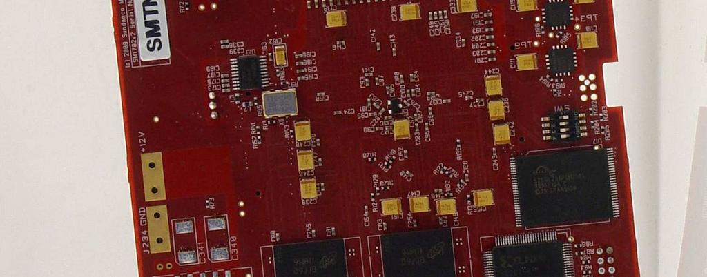
57 5 Board Layout 5.1 Top View Figure 16 - Board Layout (Top View)
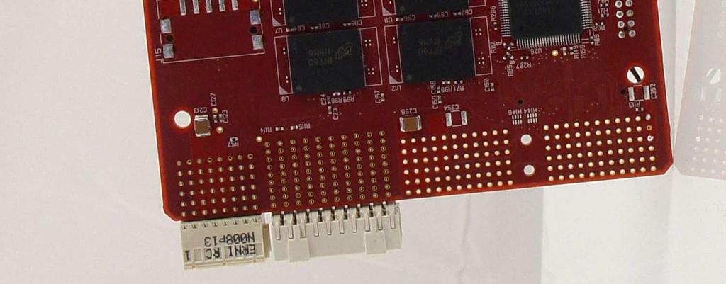
58 5.2 Bottom View Figure 17 - Board Layout (Bottom View)


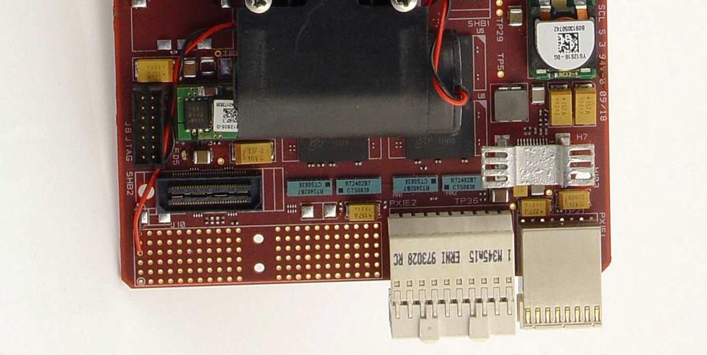
59 6 Photo 6.1 Overview of the board


60 Figure 18 - Overview of the board


61 6.2 Front panel On the front panel of the SMT702, 6 SMA connectors are available for ADC ChannelA, ADC ChannelB, External Reference and Clock in and out. There is also a dual SATA-I connector. Figure 19 - SMT702 Front Panel. 6.3 How is it going to stand on your desk? The SMT702 has been designed to be plugged into a PXI Express chassis from National Instrument The NI PXIe-1062Q is an example. Figure 20 - SMT702 - PXI Express Chassis.
.")
62 7 Software Packages Here is a list of the software packages that will be required for the SMT702 to work. SMT6300 is the software package that installs the Sundance driver for the SMT702 board. SMT6002 is the software package that installs the server application to write into flash memory (this is to store bitstreams and to reboot dynamically the board). The application is called Flash Utility. SMT7002 is the software package that installs a demo application (smt702 Configuration) for the SMT702 as shown below: As soon as the application is launched, it reads from the FPGA the board name, type of FPGA, PCB revision and the firmware version. Once running, status flags are displayed in the status section as well as the temperature of the FPGA and its internal voltages (1.0V and 2.5V). A log is available on the right hand side.
63 Figure 21 - SMT702 Demo application. Parameters to configure the clock chip and dcm phase shifts can be loaded (Hardware selection section example files are provided in \\Program Files\Sundance\SMT7026\Host\Smt702Config\Custom_Parameters) from a configuration file, as well as the clock and reference source. Samples can be stored into DDR2 memory, played back, stored into files and displayed into 2 graphs. The first one shows the raw samples and the second the FFT of the captured samples (2048 points). Each captured can be stored into individual files (smt7002_cha.txt or smt7002_chb.txt) and also a concatenated version of all captures made (smt7002_total_cha.txt or smt7002_total_chb.txt) In order to have the software source code for the SMT7002, the SMT7026 package will have to be purchased. They come as a visual C++ project with all necessary files to recompile the application and modify it.
64 8 Physical Properties Dimensions PXI Express 3U SMT702-LX110T Board Booted ADCs OFF Clock OFF SHBs OFF Board Booted ADCs ON Clock ON SHBs OFF Board Booted ADCs ON Clock ON SHBs ON Weight 272 grams Supply Currents +12V 0.88 amp amps amps. +3.3V 1.70 amps. 4.4 amps. 5.5 amps. MTBF Dimensions PXI Express 3U SMT702-FX70T Board Booted ADCs OFF Clock OFF SHBs OFF Board Booted ADCs ON Clock ON SHBs OFF Board Booted ADCs ON Clock ON SHBs ON Weight 272 grams Supply Currents +12V 0.9 amp amp amp. +3.3V 1.95 amps. 4.4 amps. 5.4 amps. MTBF The SMT7002 GUI has been used to configure the boards from which currents consumed were measured. Boards were setup as follows, internal clock locked on external 10-MHz reference, ADCs clocked at 3GSPS and set in Test mode, continuous acquisitions (DMAs).


65 9 Hardware Modification It has been found that modifying the converter reset structure improves the synchronisation between the ADCs. The non-symetrical structure previously used would add a non-wanted delay on the second ADC channels. The new structure consists in removing some ICs and replacing them by 2 sets of differential wires. ADCs can now be more accurately synchronised in frequency. A software function has been added to the software package, returning the skew between the 2 ADC sampling clocks. A typical skew measured at the FPGA is 170pS. Figure 22 - ADC Reset structure modification.
66 10 Safety This module presents no hazard to the user when in normal use. 11 EMC This module is designed to operate from within an enclosed host system, which is build to provide EMC shielding. Operation within the EU EMC guidelines is not guaranteed unless it is installed within an adequate host system. This module is protected from damage by fast voltage transients originating from outside the host system which may be introduced through the output cables. Short circuiting any output to ground does not cause the host PC system to lock up or reboot. 12 Ordering Information Three variations of this product are available: 1 SMT702 with an XC5VLX110T-3 (fastest speed grade available) FPGA and works as a PXI Express Peripheral Module. The part number for this option is SMT702. Requires a PXI Express chassis such as the NI-1062Q from National Instrument. 2 SMT702 with an XC5VLX110T-3 (fastest speed grade available) FPGA and works as a PXI Express Hybrid Peripheral Module (PXI P1 connector). The part number for this option is SMT702-HYBRPXI32. Requires a PXI Express chassis such as the NI- 1062Q from National Instrument. 3 - SMT702 with an XC5VLX110T-3 (fastest speed grade available) FPGA and works as a Compact PCI Module. The part number for this option is SMT702-CPCI32. Requires a Compact PCI rack. Note that it can also be plugged into a PXI Express chassis such as the NI-1062Q from National Instrument. 4 - SMT702 with an XC5VLX110T-3 (fastest speed grade available) FPGA and works in standalone. It can be fitted in a PCI slot (Can be PCI-32 or 64 or PCI-X on a PC motherboard) without being electrically connected to it. This option requires an external power cable and a connection to an other piece of hardware from Sundance via SHB or RSL or SATA (optional). The part number for this option is SMT702- STANDALONE. Note that the Standalone version of the SMT702 does not have any dual SATA connector. 5 SMT702 with an XC5VFX70T-3 (fastest speed grade available) FPGA and works as a PXI Express Peripheral Module. The part number for this option is SMT702- FX70T. Requires a PXI Express chassis such as the NI-1062Q from National Instrument. 6 SMT702 with an XC5VFX70T-3 (fastest speed grade available) FPGA and works as a PXI Express Hybrid Peripheral Module (PXI P1 connector). The part number for this option is SMT702-HYBRPXI32-FX70T. Requires a PXI Express chassis such as the NI-1062Q from National Instrument.

67 7 - SMT702 with an XC5VFX70T-3 (fastest speed grade available) FPGA and works as a Compact PCI Module. The part number for this option is SMT702-CPCI32-FX70T. Requires a Compact PCI rack. Note that it can also be plugged into a PXI Express chassis such as the NI-1062Q from National Instrument. 8 SMT702 with an XC5VFX100T-3 (fastest speed grade available) FPGA and works as a PXI Express Peripheral Module. The part number for this option is SMT702- FX100T. Requires a PXI Express chassis such as the NI-1062Q from National Instrument. 9 SMT702 with an XC5VFX100T-3 (fastest speed grade available) FPGA and works as a PXI Express Hybrid Peripheral Module (PXI P1 connector). The part number for this option is SMT702-HYBRPXI32-FX100T. Requires a PXI Express chassis such as the NI-1062Q from National Instrument SMT702 with an XC5VFX100T-3 (fastest speed grade available) FPGA and works as a Compact PCI Module. The part number for this option is SMT702-CPCI32- FX100T. Requires a Compact PCI rack. Note that it can also be plugged into a PXI Express chassis such as the NI-1062Q from National Instrument. Note that an SMT702 can also be used in a PC. This will require a PXIe to PCIe adaptor (Sundance part number SMT580) as show below: The SMT580 only routes the PCI express lanes, reference clock and power supplies. None of the PXI signals are routed.
Product Specification for SMT712
 Sundance Multiprocessor Technology Limited Product Specification Form : QCF51 Date : 6 July 2006 Unit / Module Description: Dual -DAC PXI Express Hybrid Peripheral Module Unit / Module Number: SMT712 Document
PXIe FPGA board SMT G Parker
 Form : QCF51 Date : 6 July 2006 PXIe FPGA board SMT700 1.5 20 th November 2009 G Parker Sundance Multiprocessor Technology Ltd, Chiltern House, Waterside, Chesham, Bucks. HP5 1PS. This document is the
APPLICATION NOTE. Application note about SMT702_SMT712 System: 2-Ghz Platform. SMT702 and SMT712 SUNDANCE MULTIPROCESSOR TECHNOLOGY LTD.
 Application note about SMT702_SMT712 System: 2-Ghz Platform SMT702 and SMT712 SUNDANCE MULTIPROCESSOR TECHNOLOGY LTD. Date Comments / Changes Author Revision 12/03/10 Original Document completed PhSR 1
User Manual for SMT784
 Sundance Multiprocessor Technology Limited User Manual Form : QCF42 Date : 11 February 2009 Unit / Module Description: Unit / Module Number: Document Issue Number: Issue Date: Original Author: Quad-ADC-14-bit-125Msps
SMT9091 SMT148-FX-SMT351T/SMT391
 Unit / Module Description: Unit / Module Number: Document Issue Number: Issue Date: Original Author: This Document provides an overview of the developed system key features. SMT148-FX-SMT351T/SMT391 E.Puillet
SMT166-FMC User Guide
 Sundance Multiprocessor Technology Limited Product Specification Unit / Module Description: Unit / Module Number: Document Issue Number: Issue Date: Original Author: SMT166-FMC User Guide Revision History
Version 1.6 Page 2 of 25 SMT351 User Manual
 SMT351 User Manual Version 1.6 Page 2 of 25 SMT351 User Manual Revision History Date Comments Engineer Version 28/07/04 First revision JPA 1.1 16/09/04 Added pin number for JP1 pinout section. Updated
SMT943 APPLICATION NOTE 1 APPLICATION NOTE 1. Application Note - SMT372T and SMT943.doc SMT943 SUNDANCE MULTIPROCESSOR TECHNOLOGY LTD.
 APPLICATION NOTE 1 Application Note - SMT372T + SMT943 SMT943 SUNDANCE MULTIPROCESSOR TECHNOLOGY LTD. Date Comments / Changes Author Revision 07/07/10 Original Document completed CHG 1 Date 13/05/2010
User Manual for SMT111
 Sundance Multiprocessor Technology Limited User Manual Form : QCF42 Date : 11 February 2009 Unit / Module Description: Standalone Carrier Board (single-module size) Unit / Module Number: SMT111 Document
User Guide of the PCIe SG DMA Engine on AVNET Virtex5 Development Board
 User Guide of the PCIe SG DMA Engine on AVNET Virtex5 Development Board V.3 Wenxue Gao weng.ziti@gmail.com 4 September 2 Revision Date Comment. 2 Aug 29 Created.. 26 Nov 29 Correction of some errors..2
SMT743 APPLICATION NOTE 1 APPLICATION NOTE 1. Application Note - SMT743 System.doc SMT743 SUNDANCE MULTIPROCESSOR TECHNOLOGY LTD.
 APPLICATION NOTE 1 Application Note - SMT743 System. SMT743 SUNDANCE MULTIPROCESSOR TECHNOLOGY LTD. Date 23/05/2011 Revision 1 Page 1 of 8 Date Comments / Changes Author Revision 23/05/11 Original Document
Sundance Multiprocessor Technology Limited. Capture Demo For Intech Unit / Module Number: C Hong. EVP6472 Intech Demo. Abstract
 Sundance Multiprocessor Technology Limited EVP6472 Intech Demo Unit / Module Description: Capture Demo For Intech Unit / Module Number: EVP6472-SMT391 Document Issue Number 1.1 Issue Data: 19th July 2012
Application Note for EVP
 Sundance Multiprocessor Technology Limited Application Note Form : QCF32 Date : 11 Februay 2009 Unit / Module Description: SMT111-SMT372T-SMT946 Unit / Module Number: Document Issue Number: 1.0 Issue Date:
DESIGN SPECIFICATION FOR SMT318-SX55. Copyright Sundance
 DESIGN SPECIFICATION FOR SMT318-SX55 Copyright Sundance All rights reserved. No part of this document may be reproduced, translated, stored in a retrieval system, or transmitted, in any form or by any
SMT338-VP. User Manual
 SMT338-VP User Manual Version 1.3 Page 2 of 22 SMT338-VP User Manual Revision History Date Comments Engineer Version 16/08/04 First revision JPA 1.0 17/05/05 Corrected: purpose of Led 5 and Led 6 SM 1.1
Sundance Multiprocessor Technology Limited. Capture Demo For Intech Unit / Module Number: C Hong. EVP6472 Intech Demo. Abstract
 Sundance Multiprocessor Technology Limited EVP6472 Intech Demo Unit / Module Description: Capture Demo For Intech Unit / Module Number: EVP6472-SMT911 Document Issue Number 1.1 Issue Data: 6th October
Virtex-II Architecture. Virtex II technical, Design Solutions. Active Interconnect Technology (continued)
") Virtex-II Architecture SONET / SDH Virtex II technical, Design Solutions PCI-X PCI DCM Distri RAM 18Kb BRAM Multiplier LVDS FIFO Shift Registers BLVDS SDRAM QDR SRAM Backplane Rev 4 March 4th. 2002 J-L
Virtex-II Architecture SONET / SDH Virtex II technical, Design Solutions PCI-X PCI DCM Distri RAM 18Kb BRAM Multiplier LVDS FIFO Shift Registers BLVDS SDRAM QDR SRAM Backplane Rev 4 March 4th. 2002 J-L
SMT-FMC211. Quad DAC FMC. Sundance Multiprocessor Technology Limited
 Sundance Multiprocessor Technology Limited Form : QCF51 Template Date : 10 November 2010 Unit / Module Description: Quad DAC FMC Unit / Module Number: Document Issue Number: 1.1 Original Issue Date: 11
Sundance Multiprocessor Technology Limited. Capture Demo For Intech Unit / Module Number: C Hong. EVP6472 Intech Demo. Abstract
 Sundance Multiprocessor Technology Limited EVP6472 Intech Demo Unit / Module Description: Capture Demo For Intech Unit / Module Number: EVP6472-SMT939 Document Issue Number 1.1 Issue Data: 1th March 2012
Prototyping NGC. First Light. PICNIC Array Image of ESO Messenger Front Page
 Prototyping NGC First Light PICNIC Array Image of ESO Messenger Front Page Introduction and Key Points Constructed is a modular system with : A Back-End as 64 Bit PCI Master/Slave Interface A basic Front-end
User Manual for DVIP
 Sundance Multiprocessor Technology Limited Form : QCF42 User Manual Date : 6 July 2006 Unit / Module Description: Unit / Module Number: DVIP (Digital Video Infrastructure Platform) System DVIP Document
New! New! New! New! New!
 New! New! New! New! New! Models 72664, Model 74664 Model 73664 General Information Models 72664, are members of the Cobalt family of high-performance CompactPCI s based on the Xilinx Virtex-6 FPGA. They
cpci-dart Base-Board & Daughter-Board
 DYNAMIC ENGINEERING 150 DuBois, Suite C Santa Cruz, CA 95060 (831) 457-8891 Fax (831) 457-4793 http://www.dyneng.com sales@dyneng.com Est. 1988 User Manual cpci-dart Base-Board & Daughter-Board Eight-Channel
ADQ412. Product Preview. Features. Introduction. Applications. Software support. Ordering information. ADQ Development Kit
 ADQ412 is a software-selectable two or four channel flexible member of the ADQ V6 Digitizer family. The ADQ412 has an outstanding combination of high bandwidth and dynamic range, which enables demanding
Product Information Sheet PX Channel, 14-Bit Waveform Digitizer
 Product Information Sheet PX14400 2 Channel, 14-Bit Waveform Digitizer FEATURES 2 Analog Channels at up to 400 MHz Sample Rate per Channel 14 Bits of Resolution Bandwidth from 100 KHz to 400 MHz 1 Gigabyte
User Manual for FC100
 Sundance Multiprocessor Technology Limited User Manual Form : QCF42 Date : 6 July 2006 Unit / Module Description: IEEE-754 Floating-point FPGA IP Core Unit / Module Number: FC100 Document Issue Number:
Zynq AP SoC Family
 Programmable Logic (PL) Processing System (PS) Zynq -7000 AP SoC Family Cost-Optimized Devices Mid-Range Devices Device Name Z-7007S Z-7012S Z-7014S Z-7010 Z-7015 Z-7020 Z-7030 Z-7035 Z-7045 Z-7100 Part
The Next Generation 65-nm FPGA. Steve Douglass, Kees Vissers, Peter Alfke Xilinx August 21, 2006
 The Next Generation 65-nm FPGA Steve Douglass, Kees Vissers, Peter Alfke Xilinx August 21, 2006 Hot Chips, 2006 Structure of the talk 65nm technology going towards 32nm Virtex-5 family Improved I/O Benchmarking
PXDAC4800. Product Information Sheet. 1.2 GSPS 4-Channel Arbitrary Waveform Generator FEATURES APPLICATIONS OVERVIEW
 Product Information Sheet PXDAC4800 1.2 GSPS 4-Channel Arbitrary Waveform Generator FEATURES 4 AC-Coupled or DC-Coupled DAC Channel Outputs 14-bit Resolution @ 1.2 GSPS for 2 Channels or 600 MSPS for 4
Using the FADC250 Module (V1C - 5/5/14)
") Using the FADC250 Module (V1C - 5/5/14) 1.1 Controlling the Module Communication with the module is by standard VME bus protocols. All registers and memory locations are defined to be 4-byte entities.
Using the FADC250 Module (V1C - 5/5/14) 1.1 Controlling the Module Communication with the module is by standard VME bus protocols. All registers and memory locations are defined to be 4-byte entities.
Product Specification for SMT148FX
 Sundance Multiprocessor Technology Limited Product Specification Form : QCF51 Date : 6 July 2006 Unit / Module Description: 4 Slot Stand Alone TIM carrier Unit / Module Number: SMT148FX Document Issue
User Guide of the PCIe SG DMA Engine on Xilinx ML605 Virtex6 Development Board
 User Guide of the PCIe SG DMA Engine on Xilinx ML65 Virtex6 Development Board V1.7 Wenxue Gao weng.ziti@gmail.com Sabatini Simone sabatini.simone@gmail.com 26 March 212 Revision Date Comment 1. 2 Aug 29
AD GSPS Analog Input XMC/PMC with Xilinx Virtex -5 FPGA. Data Sheet
 Data Sheet 3GSPS Analog Input XMC/PMC with Xilinx Virtex -5 FPGA Applications Electronic Warfare (EW) Spectral Analysis RADAR Features 3GSPS, 8-bit ADC Xilinx Virtex-5 SX95T FPGA (user programmable) Dual
HCAL DCC Technical Reference E. Hazen - Revised March 27, 2007 Note: Latest version of this document should be available at:
 HCAL DCC Technical Reference E. Hazen - Revised March 27, 2007 Note: Latest version of this document should be available at: http://cmsdoc.cern.ch/cms/hcal/document/countinghouse/dcc/dcctechref.pdf Table
ADM-XRC-5LX. PCI Mezzanine Card. User Guide. Version 2.0
 ADM-XRC-5LX PCI Mezzanine Card User Guide Copyright 2006, 2007, 2008 Alpha Data Parallel Systems Ltd. All rights reserved. This publication is protected by Copyright Law, with all rights reserved. No part
Revision History. Changes Made Issue Initials 1.1 PSR. (impedances) 1.3 PSR. register descriptions. 1.7 PSR. PLL register (0x2) corrected.
 1.3 PSR. register descriptions. 1.7 PSR. PLL register (0x2) corrected.") SMT350 User Manual Version 1.9 Page 2 of 45 SMT350 User Manual Revision History Changes Made Issue Initials 11/10/05 Original Document. 1.0 PSR 18/01/06 Updates on ADC inputs and DAC outputs (impedances)
SMT350 User Manual Version 1.9 Page 2 of 45 SMT350 User Manual Revision History Changes Made Issue Initials 11/10/05 Original Document. 1.0 PSR 18/01/06 Updates on ADC inputs and DAC outputs (impedances)
UWB PMC/XMC I/O Module
 UWB PMC/XMC I/O Module 2 Ch. Ultra-Wide-Band Receiver 25 MSPS A/Ds Large FPGA for User Code Deep memory Features Two LTC222-2, 2-bit 25MSPS converters 3MHz analog input bandwidth Support for undersampling
X5-TX. Datasheet. AmpliconBenelux.com
 V 2.0 11/10/09 PCI Express XMC Module with Four channels 500 MSPS or Dual 1 GSPS, 16-bit DAC outputs, Virtex5 FPGA with 512MB DDR2 DRAM and 4 MB QDR SRAM Memories FEATURES 16-bit DACs: Four outputs at
SMT370v2/v3 User Manual
 SMT370v2/v3 User Manual User Manual (QCF42); Version 3.0, 8/11/00; Sundance Multiprocessor Technology Ltd. 1999 Version 2.0 Page 2 of 46 SMT370v2/v3 User Manual Revision History Date Comments Engineer
Field Programmable Gate Array (FPGA)
") Field Programmable Gate Array (FPGA) Lecturer: Krébesz, Tamas 1 FPGA in general Reprogrammable Si chip Invented in 1985 by Ross Freeman (Xilinx inc.) Combines the advantages of ASIC and uc-based systems
Field Programmable Gate Array (FPGA) Lecturer: Krébesz, Tamas 1 FPGA in general Reprogrammable Si chip Invented in 1985 by Ross Freeman (Xilinx inc.) Combines the advantages of ASIC and uc-based systems
7-Series Architecture Overview
 7-Series Architecture Overview Zynq Vivado 2013.2 Version This material exempt per Department of Commerce license exception TSU Objectives After completing this module, you will be able to: Describe the
Analog & Digital I/O
 Analog & Digital I/O ANALOG & DIGITAL I/O MODEL DESCRIPTION Cobalt 730 1 GHz and D/A, Virtex-6 - XMC Cobalt 78630 1 GHz and D/A, Virtex-6 - x8 Cobalt 53630 1 GHz and D/A, Virtex-6-3U VPX - Format 1 Cobalt
S2C K7 Prodigy Logic Module Series
 S2C K7 Prodigy Logic Module Series Low-Cost Fifth Generation Rapid FPGA-based Prototyping Hardware The S2C K7 Prodigy Logic Module is equipped with one Xilinx Kintex-7 XC7K410T or XC7K325T FPGA device
UniBoard V1.0 Board Description
 V1.0 Board Description Auteur(s) / Author(s): Organisatie / Organization Datum / Date Sjouke Zwier Gijs Schoonderbeek ASTRON 24-06-2010 Controle / Checked: ASTRON Goedkeuring / Approval: ASTRON Autorisatie
Revision History. Changes Made Issue Initials. 02/09/08 Original Document based on SMT350 User Manual 1.0 PhSR
 SMT950 User Manual Version 2.0 Page 2 of 52 SMT950 User Manual Revision History Changes Made Issue Initials 02/09/08 Original Document based on SMT350 User Manual 1.0 PhSR 21/11/09 Update ADC DC coupling
Summary. Introduction. Application Note: Virtex, Virtex-E, Spartan-IIE, Spartan-3, Virtex-II, Virtex-II Pro. XAPP152 (v2.1) September 17, 2003
 September 17, 2003") Application Note: Virtex, Virtex-E, Spartan-IIE, Spartan-3, Virtex-II, Virtex-II Pro Xilinx Tools: The Estimator XAPP152 (v2.1) September 17, 2003 Summary This application note is offered as complementary
Application Note: Virtex, Virtex-E, Spartan-IIE, Spartan-3, Virtex-II, Virtex-II Pro Xilinx Tools: The Estimator XAPP152 (v2.1) September 17, 2003 Summary This application note is offered as complementary
VXS-610 Dual FPGA and PowerPC VXS Multiprocessor
 VXS-610 Dual FPGA and PowerPC VXS Multiprocessor Two Xilinx Virtex -5 FPGAs for high performance processing On-board PowerPC CPU for standalone operation, communications management and user applications
CompuScope Ultra-fast waveform digitizer card for PCI bus. APPLICATIONS. We offer the widest range of
 We offer the widest range of high-speed and high-resolution digitizers available on the market CompuScope 1602 Ultra-fast waveform digitizer card for PCI bus today. Our powerful PC-based instrumentation
Basic FPGA Architecture Xilinx, Inc. All Rights Reserved
 Basic FPGA Architecture 2005 Xilinx, Inc. All Rights Reserved Objectives After completing this module, you will be able to: Identify the basic architectural resources of the Virtex -II FPGA List the differences
AGM CPLD AGM CPLD DATASHEET
 AGM CPLD DATASHEET 1 General Description AGM CPLD family provides low-cost instant-on, non-volatile CPLDs, with densities from 256, 272 to 576 logic LUTs and non-volatile flash storage of 256Kbits. The
14HSAI4. 14-Bit, 4-Channel, 50MSPS/Channel PMC Analog Input Board. With 66MHz PCI Compatibility, Multiple Ranges, and Data Packing
 14HSAI4 14-Bit, 4-Channel, 50MSPS/Channel PMC Analog Input Board FEATURES: With 66MHz PCI Compatibility, Multiple Ranges, and Data Packing Available in PMC, PCI, cpci and PC104-Plus and PCI Express form
New! New! New! New! New!
 New! New! New! New! New! Model 5950 Features Supports Xilinx Zynq UltraScale+ RFSoC FPGAs 18 GB of DDR4 SDRAM On-board GPS receiver PCI Express (Gen. 1, 2 and 3) interface up to x8 LVDS connections to
64-Channel, 16-Bit Simultaneous Sampling PMC Analog Input Board
 66-16AI64SSA/C 64-Channel, 16-Bit Simultaneous Sampling PMC Analog Board With 200 KSPS Sample Rate per Channel and 66 MHz PCI Support Available in PMC, PCI, cpci and PC104-Plus and PCI Express form factors
Product Information Sheet PDA14 2 Channel, 14-Bit Waveform Digitizer APPLICATIONS FEATURES OVERVIEW
 Product Information Sheet PDA 2 Channel, -Bit Waveform Digitizer FEATURES 2 Channels at up to 100 MHz Sample Rate Bits of Resolution Bandwidth from DC-50 MHz 512 Megabytes of On-Board Memory 500 MB/s Transfer
New Software-Designed Instruments
 1 New Software-Designed Instruments Nicholas Haripersad Field Applications Engineer National Instruments South Africa Agenda What Is a Software-Designed Instrument? Why Software-Designed Instrumentation?
8. Migrating Stratix II Device Resources to HardCopy II Devices
 8. Migrating Stratix II Device Resources to HardCopy II Devices H51024-1.3 Introduction Altera HardCopy II devices and Stratix II devices are both manufactured on a 1.2-V, 90-nm process technology and
C900 PowerPC G4+ Rugged 3U CompactPCI SBC
 C900 PowerPC G4+ Rugged 3U CompactPCI SBC Rugged 3U CompactPCI SBC PICMG 2.0, Rev. 3.0 Compliant G4+ PowerPC 7447A/7448 Processor @ 1.1 Ghz with AltiVec Technology Marvell MV64460 Discovery TM III System
Product Information Sheet PDA16 2 Channel, 16-Bit Waveform Digitizer
 Product Information Sheet PDA16 2 Channel, 16-Bit Waveform Digitizer FEATURES 2 Analog Channels at up to 160 MHz Sample Rate per Channel 16 Bits of Resolution Bandwidth from 100 KHz to 700 MHz 512 Megabytes
The Benefits of FPGA-Enabled Instruments in RF and Communications Test. Johan Olsson National Instruments Sweden AB
 The Benefits of FPGA-Enabled Instruments in RF and Communications Test Johan Olsson National Instruments Sweden AB 1 Agenda Introduction to FPGAs in test New FPGA-enabled test applications FPGA for test
14-Bit, 4-Channel, 50MSPS/Channel PMC Analog Input Board
 PMC66-14HSAI4 14-Bit, 4-Channel, 50MSPS/Channel PMC Analog Input Board With 66MHz PCI Compatibility, Multiple Ranges, and Data Packing Available also in PCI, cpci and PC104-Plus form factors as: PCI66-14HSAI4:
ML505 ML506 ML501. Description. Description. Description. Features. Features. Features
 ML501 Purpose: General purpose FPGA development board. Board Part Number: HW-V5-ML501-UNI-G Device Supported: XC5VLX50FFG676 Price: $995 The ML501 is a feature-rich and low-cost evaluation/development
SMT407 User Manual User Manual; Version 1.0.2, 4/8/04; Sundance Digital Signal Processing, Inc. 2004
 SMT407 User Manual User Manual; Version 1.0.2, 4/8/04; Sundance Digital Signal Processing, Inc. 2004 Version 1.0.0 Page 2 of 38 SMT407 User Manual Revision History Date Comments Engineer Version 2/28/05
5I24 ANYTHING I/O MANUAL
 5I24 ANYTHING I/O MANUAL Version 1.5 This page intentionally not blank Table of Contents GENERAL.......................................................... 1 DESCRIPTION.................................................
XMC-FPGA05F. Programmable Xilinx Virtex -5 FPGA PMC/XMC with Quad Fiber-optics. Data Sheet
 Data Sheet XMC-FPGA05F Programmable Xilinx Virtex -5 FPGA PMC/XMC with Quad s Applications Remote Sensor Interface Data Recorders Distributed Processing Interconnect Protocol Converter Data Encryption
Product Information Sheet PX14400D 2 Channel, DC-Coupled, 14-Bit Digitizer
 Product Information Sheet PX14400D 2 Channel, DC-Coupled, 14-Bit Digitizer Fsab FEATURES 2 Analog Channels at up to 400 MHz Sample Rate per Channel 14 Bits of Resolution Bandwidth from DC to 200 MHz 200
PC104P-24DSI Channel 24-Bit Delta-Sigma PC104-Plus Analog Input Board
 PC104P-24DSI12 12-Channel 24-Bit Delta-Sigma PC104-Plus Analog Input Board With 200 KSPS Sample Rate per Channel and Optional Low-Power Configuration Available also in PCI, cpci and PMC form factors as:
XMC-24DSI24WRC Wide-Range 24-Bit, 24-Channel, 200KSPS XMC Analog Input Module With 24 Wide-Range (High-Level, Low-Level) Delta-Sigma Input Channels
 Delta-Sigma Input Channels") XMC-24DSI24WRC Wide-Range 24-Bit, 24-Channel, 200KSPS XMC Analog Input Module With 24 Wide-Range (High-Level, Low-Level) Delta-Sigma Input Channels Features Include: 24 wide-range differential 24-Bit simultaneously-sampled
XMC-24DSI24WRC Wide-Range 24-Bit, 24-Channel, 200KSPS XMC Analog Input Module With 24 Wide-Range (High-Level, Low-Level) Delta-Sigma Input Channels Features Include: 24 wide-range differential 24-Bit simultaneously-sampled
12-Channel, 12-Bit PMC Analog Input/Output Board
 12-Channel, 12-Bit PMC Analog Input/Output Board With Eight Simultaneously-Sampled Wide-Range Inputs at 2.0 MSPS per Channel, Four Analog Outputs, and 16-Bit Digital I/O Port Available also in PCI, cpci
FPGA for Complex System Implementation. National Chiao Tung University Chun-Jen Tsai 04/14/2011
 FPGA for Complex System Implementation National Chiao Tung University Chun-Jen Tsai 04/14/2011 About FPGA FPGA was invented by Ross Freeman in 1989 SRAM-based FPGA properties Standard parts Allowing multi-level
INTRODUCTION TO FPGA ARCHITECTURE
 3/3/25 INTRODUCTION TO FPGA ARCHITECTURE DIGITAL LOGIC DESIGN (BASIC TECHNIQUES) a b a y 2input Black Box y b Functional Schematic a b y a b y a b y 2 Truth Table (AND) Truth Table (OR) Truth Table (XOR)
16-Bit, 12-Channel, 2-MSPS PMC Analog Input/Output Board
 66-16AISS8AO4 16-Bit, 12-Channel, 2-MSPS PMC Analog Input/Output Board With Eight Simultaneously Sampled Analog Inputs, Four Analog Outputs, and Input Sampling Rates to 2.0 MSPS per channel Available in
New! New! New! New! New!
 New! New! New! New! New! Model 5950 Features Supports Xilinx Zynq UltraScale+ RFSoC FPGAs 18 GB of DDR4 SDRAM On-board GPS receiver PCI Express (Gen. 1, 2 and 3) interface up to x8 LVDS connections to
Schematic. A: Overview of the Integrated Detector Readout Electronics and DAQ-System. optical Gbit link. 1GB DDR Ram.
 A: Overview of the Integrated Detector Readout Electronics and DAQ-System N s CASCADE Detector Frontend (X0) (X) (Y0) (Y) optional: CIPix- Board (T) Optical Gigabit Link CDR.0 FPGA based readout board
FPGA Provides Speedy Data Compression for Hyperspectral Imagery
 FPGA Provides Speedy Data Compression for Hyperspectral Imagery Engineers implement the Fast Lossless compression algorithm on a Virtex-5 FPGA; this implementation provides the ability to keep up with
High-Value PXI Embedded Controller for Windows. High-Value Embedded Controllers for PXI Express NI PXI-8101, NI PXI NI PXIe-8101, NI PXIe-8102
 High-Value PXI Embedded Controller for Windows NI PXI-8101, NI PXI-8102 2.0 GHz single-core for PXI-8101, 1.9 GHz dual-core for PXI-8102 1 GB (1 x 1 GB DIMM) 800 MHz DDR2 RAM standard, 4 GB (1 x 4 GB DIMMs)
CMX18 FEATURES A 18-SLOT 3U PXI EXPRESS CHASSIS
 83-0062-000 15A D A T A S H E E T CMX18 18-SLOT 3U PXI EXPRESS CHASSIS FEATURES 18-slot PXI Express chassis with 1 system controller slot, 6 peripheral slots, 10 hybrid slots, and 1 timing slot High bandwidth
cpci6u-24dsi32r 32-Channel 24-Bit Delta-Sigma Analog Input Board
 cpci6u-24dsi32r 32-Channel 24-Bit Delta-Sigma Analog Input Board FEATURES: 32 Differential 24-Bit Analog Input Channels Delta-Sigma Converter per Channel, with Linear Phase Digital Antialias Filtering
Calypso-V6 VME / VXS. Extreme Signal Acquisition. and FPGA-based Processing. Without Compromise
 The Leader In FPGA-based Sensor I/O Processing Calypso-V6 VME / VXS Extreme Signal Acquisition and FPGA-based Processing Without Compromise Features Two 12-bit ADCs at 3.6 GSPS Also supports 6 channels
ADM-XRC-5TZ. PCI Mezzanine Card. User Guide. Version 2.0
 ADM-XRC-5TZ PCI Mezzanine Card User Guide Copyright 2007-2009 Alpha Data Parallel Systems Ltd. All rights reserved. This publication is protected by Copyright Law, with all rights reserved. No part of
Simplify System Complexity
 Simplify System Complexity With the new high-performance CompactRIO controller Fanie Coetzer Field Sales Engineer Northern South Africa 2 3 New control system CompactPCI MMI/Sequencing/Logging FieldPoint
24DSI16WRC Wide-Range 24-Bit, 16-Channel, 105KSPS Analog Input Module With 16 Wide-Range (High-Level, Low-Level) Delta-Sigma Input Channels
 Delta-Sigma Input Channels") 24DSI16WRC Wide-Range 24-Bit, 16-Channel, 105KSPS Analog Input Module With 16 Wide-Range (High-Level, Low-Level) Delta-Sigma Input Channels Features Include: Available in PMC, PCI, cpci and PC104-Plus
24DSI16WRC Wide-Range 24-Bit, 16-Channel, 105KSPS Analog Input Module With 16 Wide-Range (High-Level, Low-Level) Delta-Sigma Input Channels Features Include: Available in PMC, PCI, cpci and PC104-Plus
PCI-16HSDI: 16-Bit, Six-Channel Sigma-Delta Analog Input PMC Board. With 1.1 MSPS Sample Rate per Channel, and Two Independent Clocks
 PMC-16HSDI 16-Bit, Six-Channel Sigma-Delta Analog Input PMC Board With 1.1 MSPS Sample Rate per Channel, and Two Independent Clocks Available also in PCI, cpci and PC104-Plus form factors as: PCI-16HSDI:
PMC66-18AI32SSC1M: PMC, Single-width
 66-18AI32SSC1M 18-Bit, 32-Channel, Differential, 1.0 MSPS, Simultaneous Sampling PMC Analog Input Board With 1.0 MSPS Sample Rate per Channel and 66 MHz PCI Support Available in PMC, PCI, cpci and PC104-Plus
16AIO Bit Analog Input/Output Board. With 16 Input Channels and 8 Output Channels
 16AIO168 16-Bit Analog Input/Output Board With 16 Input Channels and 8 Output Channels Available in PMC, PCI, cpci, PCI-104 and PC104-Plus and PCI Express form factors as: PMC-16AIO168: PMC, Single-width
FMC150 User Manual r1.9 FMC150. User Manual. Abaco Systems, USA. Support Portal
 FMC150 User Manual Abaco Systems, USA Support Portal This document is the property of Abaco Systems and may not be copied nor communicated to a third party without the written permission of Abaco Systems.
C901 PowerPC MPC7448 3U CompactPCI SBC
 C901 PowerPC MPC7448 3U CompactPCI SBC Rugged 3U CompactPCI SBC PowerPC 7448 @ 1.4 GHz, 1.0 GHz, or 600 MHz, with AltiVec Technology 166 MHz MPX Bus Marvell MV64460 Discovery TM III System Controller One
FM680 User Manual V1.4 FM680. User Manual for Virtex-6 XMC card
 FM680 User Manual for Virtex-6 XMC card 4DSP LLC, 955 S Virginia Street, Suite 214, Reno, NV 89502, USA 4DSP BV,Ondernemingsweg 66f, 2404 HN, Alphen a/d Rijn, Netherlands Email: support@4dsp.com This document
SMT148. User Manual. Sundance Digital Signal Processing Inc 4790 Caughlin Parkway #233, Reno, NV , USA.
 SMT148 User Manual Sundance Digital Signal Processing Inc 4790 Caughlin Parkway #233, Reno, NV 89509-0907, USA. Version 1.4 Page 2 of 35 SMT148 User Manual Revision History Date Comments Engineer Version
LogiCORE IP Initiator/Target v5 and v6 for PCI-X
 LogiCORE IP Initiator/Target v5 and v6 for PCI-X DS208 April 19, 2010 Introduction The LogiCORE IP Initiator/Target v5 and v6 for PCI -X core interface is a pre-implemented and fully tested module for
CPCI-IPC. Intelligent DSP Based Dual IndustryPack Carrier for CompactPCI systems REFERENCE MANUAL Version 2.
 CPCI-IPC Intelligent DSP Based Dual IndustryPack Carrier for CompactPCI systems REFERENCE MANUAL 724-20-000-4000 Version 2.0 May 1998 ALPHI TECHNOLOGY CORPORATION 6202 S. Maple Avenue #120 Tempe, AZ 85283
Speedster22i FPGA Family Power Estimator Tool User Guide. UG054- July 28, 2015
 Speedster22i FPGA Family Power Estimator Tool User Guide UG054- July 28, 2015 1 UG054, July 28, 2015 Copyright Info Copyright 2015 Achronix Semiconductor Corporation. All rights reserved. Achronix is a
Using PEX 8648 SMA based (SI) Card
 Card") Using PEX 8648 SMA based (SI) Card White Paper Version 1.3 July 2010 Website: Technical Support: www.plxtech.com www.plxtech.com/support Copyright 2008 by PLX Technology, Inc. All Rights Reserved Version
Using PEX 8648 SMA based (SI) Card White Paper Version 1.3 July 2010 Website: Technical Support: www.plxtech.com www.plxtech.com/support Copyright 2008 by PLX Technology, Inc. All Rights Reserved Version
PMX09 DATA SHEET FEATURES A PORTABLE 9-SLOT 3U PXI EXPRESS CHASSIS WITH INTEGRATED DISPLAY AND KEYBOARD
 83-0039-000 14A DATA SHEET PMX09 PORTABLE 9-SLOT 3U PXI EXPRESS CHASSIS WITH INTEGRATED DISPLAY AND KEYBOARD FEATURES 9-slot PXI Express chassis with 1 system controller slot, 6 peripheral slots, 1 hybrid
Zynq-7000 All Programmable SoC Product Overview
 Zynq-7000 All Programmable SoC Product Overview The SW, HW and IO Programmable Platform August 2012 Copyright 2012 2009 Xilinx Introducing the Zynq -7000 All Programmable SoC Breakthrough Processing Platform
64-Channel, 16-Bit Simultaneous Sampling PMC Analog Input Board
 PMC66-16AI64SSA/C 64-Channel, 16-Bit Simultaneous Sampling PMC Analog Board With 200 KSPS Sample Rate per Channel and 66 MHz PCI Support 64 Analog s with Dedicated 200KSPS 16-Bit ADC per Channel Simultaneous
PC104P-24DSI6LN. Six-Channel Low-Noise 24-Bit Delta-Sigma PC104-Plus Analog Input Module. With 200 KSPS Sample Rate per Channel
 PC104P-24DSI6LN Six-Channel Low-Noise 24-Bit Delta-Sigma PC104-Plus Analog Input Module With 200 KSPS Sample Rate per Channel Available also in PCI, cpci and PMC form factors as: PCI-24DSI6LN: cpci-24dsi6ln:
CHAMP-FX2. FPGA Accelerator Signal Processing Platform. Data Sheet. Features 6U VPX-REDI (VITA 46 and 48) FPGA signal processing platform
 FPGA signal processing platform") Data Sheet CHAMP-FX2 FPGA Accelerator Signal Processing Platform Features 6U VPX-REDI (VITA 46 and 48) FPGA signal processing platform Two user-programmable Xilinx Virtex -5 FPGA nodes (LX110T or LX220T)
Data Sheet CHAMP-FX2 FPGA Accelerator Signal Processing Platform Features 6U VPX-REDI (VITA 46 and 48) FPGA signal processing platform Two user-programmable Xilinx Virtex -5 FPGA nodes (LX110T or LX220T)
Subject: Jumper, DIP and optional resistor settings for ROACH rev Location of jumpers, switches and resistors on hardware
 Technical Memo Number: NRF-KAT7-5.0-MEM-008 To : DBE Team From : Jason Manley, Francois Kapp, David George Date : 20 May 2009 Subject: Jumper, DIP and optional resistor settings for ROACH rev 1.02 Location
PowerPlay Early Power Estimator User Guide for Cyclone III FPGAs
 PowerPlay Early Power Estimator User Guide for Cyclone III FPGAs 101 Innovation Drive San Jose, CA 95134 www.altera.com Software Version: QII v9.0 SP2 Document Version: 2.0 Document Date: June 2009 UG-01013-2.0
CPCI-AD32. Intelligent DSP Based 32 Channel Analog Input Card for 3U CompactPCI systems REFERENCE MANUAL Version 1.
 CPCI-AD32 Intelligent DSP Based 32 Channel Analog Input Card for 3U CompactPCI systems REFERENCE MANUAL 751-10-000-4000 Version 1.0 September 1998 ALPHI TECHNOLOGY CORPORATION 6202 S. Maple Avenue #120