Version 02 Mezzanine on the 16MB board
|
|
|
- Daniel Mitchell Gibbs
- 5 years ago
- Views:
Transcription
1 Version 02 Mezzanine on the 16MB board Thoughts and notes:- CY62167DV30 needs to be connected to a total of 21 address lines to fully decode each of the 2M x 8bit bytes AS6C3216 needs to be connected to a total of 22 address lines to fully decode each of the 4M x 8bit bytes Only the AS6C3216 chip uses Pin 10, therefore Pin 10 should be the highest address bit!! Both the CY62167DV30 and AS6C3216 use Pin 45 (in byte mode) as an address input, this should be the next address below that used on pin10 Taking mezzanine (byte) interleaving (ba0) into account (2 mezzanines) CY62167DV30 needs buffered addresses ba1 to ba20 to be connected to chip A0 to A19, ba21 should be connected to Pin 45 AS6C3216 needs buffered addresses ba1 to ba20 to be connected to chip A0 to A19, ba21 should be connected to Pin 45 & ba22 should be connected to Pin10 In the case of CY62167DV30 ba22 & ba23 is decoded by U4a to address 4 chips per mezzanine ( A*, B*, C* & D*) In the case of AS6C3216 only ba23 is decoded by U4a (see previous sent doc for mod details) Summary We only need be concerned that Pin 45 of the SRAM is ba21, and Pin 10 of the SRAM (AS6C..) is ba22

2
3
4 On the two diagrams above ignore the black net names ba...etc, I have superimposed onto the connector pins the actual SRAM pinout to see how things line up with a V02 mezzanine (2 nd March 2014) on the 16MB SRAM Board (23 rd March 2014). Comparing the two images we see that addresses A0 to A16 line up perfectly then A17 to A19 things go wobbly, the order of these pins doesnt matter as long as they stay within the range ba18 ba20 as mentioned in the notes above. Our only problem chip address line is A17 (Pin 37 of the header) this needs to be connected to ba20 to fullfill the above requirements then all will be OK. We note also that Header Pin 40 which connects to SRAM chip Pin 45 can also be jumpered for ba21 fullfilling the requirement for both SRAM chips. SO... the V02 mezzanine can be patched for the CY62167DV30 by linking mezzanine pins 35 and 37 together as you have already indicated on your website because Pin 10 of the CY62167DV30 is not connected to anything... BUT... this mezzanine is not usable for the AS6C3216 because by default Mezzanine Pin 35 which connects to Pin 10 of the SRAM chip which in the case of the AS6C3216 needs to be ba22!! Possible fix :- transpose pins 35 and 37 on the mezzanine PCB so that SRAM Pin 10 comes out on Header Pin 37, then jumper block K3 pin 3 could be changed to ba22 making is easier to use both types of memory on the same mezzanine.
5 Version 6 Mezzanine on the 16MB board
6 Now lets look at the version 6 mezzanine:- Again ignoring the black net names ba...etc, I have superimposed onto the mezzanine connector pins the actual SRAM pinout to see how the V6 mezzanine (2 nd March 2014) lines up with the 16MB SRAM Board (23 rd March 2014). Comparing the image above with the SRAM board header picture above we can see that the chip address lines A0 to A16 line up perfectly, A17 now follows on in sequence connected to ba18 on the SRAM board, A18 and A19 also follow in sequence connected to SRAM board ba19 and ba20 respectively. Pin 45 of the SRAM chip connects to Pin 40 of the header making it jumperable on K4 to ba21 Perfect! Pin 10 of the SRAM chip connects to Pin 37 of the header permitting wire patching to ba22 on the SRAM board for the AS6C3216 chip. (K3 Pin 3 needs to be changed to ba22 in a future version of the SRAM board) SO... the version 6 mezzanine will work with the CY62167DV30 on the 16MB SRAM V1 board without modification. The version 6 mezzanine can also be used to take the AS6C3216 SRAM chips with a little patching on the 16MB SRAM V1 board (see notes below) to reduce chip count and save money.
7 Modifiying the 16MB SRAM V01 Board to take the AS6C3216 First let it be said that this modification is for those users who are confident in their abilities to carry out the necessary patches and also have a full understanding of the theory behind the modification and all the notes listed in this document (above), It is not intended for the novice builder. These memory chips are expensive and mistakes can be very costly, It is advise to print out this document and study it in detail before you decide to invest in this modification. A later version/release of the 16MB SRAM board may include these modifications but this will likely not be for some time to come. Theory of operation :- In its normal un-modified form the 16MB SRAM board has been designed to take 8 x 2MB SRAM chips (CY62167DV30) laid out on 2 mezzanine panels which plug onto the SRAM main board, 4 chips per mezzanine. Looking at the mezzanine header pins 23,25,27,29 we notice 4 chip select lines A*, B*, C* & D*, each one selecting one of the 4 SRAM chips mounted on the mezzanine. These lines are also commoned between the two mezzanine panels to enable 2 chips to be addressed at one time for 16 bit operation. For 8 bit operation the read/write signals on Pins 19 & 21 are gated/steered through the 8/16 bit data selection circuit (U9, U12, U13 etc...) which facilitates the interleaving of the two mezzanines, one mezzanine for odd addresses the other for even.. Therefore if we wish to use a higher capacity SRAM chip such as the AS6C3216 to reduce chip count and hence cost, we need to mount two chips on each mezzanine to maintain functionality for 8 and 16 bit mode. If all 4 chip were mounted on one mezzanine, in 16 bit mode we would only have half of a 16 bit word, and in 8 bit mode we would have only odd OR even address locations.
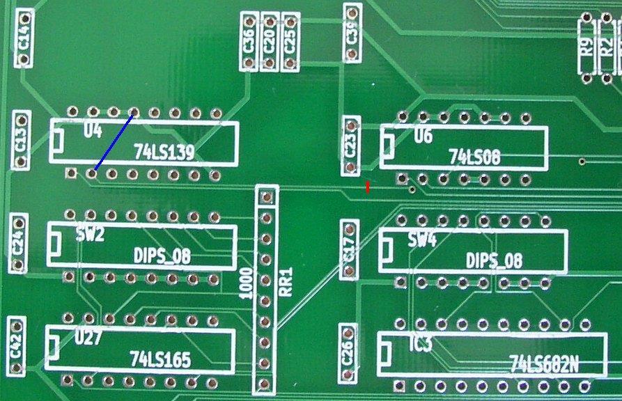
8 Looking at the truth table above for U4A we can see how the chip select lines (A*, B*, C* & D*) are generated from address lines ba23 and ba22 for the 4 SRAM chips on each mezzanine. In order to use the higher capacity AS6C2316 4MB SRAM chip we need to redirect ba22 onto Pin 37 of the mezzanine header and facilitate a way of producing just two chip select outputs. Taking note of the dotted red line which diagramatically shows the address range area of the two AS6C2316 SRAM chips, we can see that ba23 can be used to generate the 2 chip select lines we require if we suppress the changes on A0 (Pin 2 of U4A) by strapping it to ground. The blue boxed areas in column A0 can just be thought of as 2 x 2MB pages inside the 4MB SRAM chip. We achieve the desired result by cutting a trace (ba22) leading to Pin 2 of U4A and pulling Pin 2 to ground, our two chip select lines will then be A* and C* (because A0 is tied low) and this determines the locations on the mezzanine panels where we need to solder our SRAM chips.
9 U4A SRAM Chip Select Decoder The diagram above shows the changes to U4A discussed above in schematic form, the red line indicates a cut in the signal trace ba22, pin 2 is then tied to GND. The picture below shows the best location to cut the signal trace ba22 that feeds pin 2 of U4, the red line indicates component side, and the blue line indicates where to add the wire link to ground pin 2 of U4, this will need to be mounted on the copper (non- component side) Note:- Pins 8, 13, 14, & 15 are all ground, diagram shows pin 13 for reasons of clarity.
10

11 The remaining two wire links pick up address line ba22 and connect it to Pin 37 on each mezzanine header via jumpers K3 and K6 Solder one wire link from Pin 2 of jumper P49 to Pin 2 of jumper K3 Solder the other link from Pin 2 of jumper P49 to Pin 2 of jumper K6 This completes the wire link patches.

12 Finally solder 2 x AS6C3216 SRAM chips into locations U9 and U32 on each of the two mezzanines (4 chips in total) as shown in to picture below taking care to observe the correct orientation of Pin 1, mistakes are costly at $22 approx per chip. Take care to ensure that the 16MB SRAM board is jumpered for 3.3v memory devices (K2, 1-2 and K5, 1-2) Then fit both mezzanines to the 16MB SRAM board and check other board configuration jumpers and set as necessary. You should now have a full 16MB RAM address range at just over half the cost of using the Cypress CY62167DV30 The AS6C3216 is available from Digikey part number ND at approx $21.00 each
KNJN I2C bus development boards
 KNJN I2C bus development boards 2005, 2006, 2007, 2008 KNJN LLC http://www.knjn.com/ Document last revision on December 5, 2008 R22 KNJN I2C bus development boards Page 1 Table of Contents 1 The I2C bus...4
Two-Chip 32k in the TI-99/4A Console by Mike Brent Updated: 27 Jul 2016
 Two-Chip 32k in the TI-99/4A Console by Mike Brent Updated: 27 Jul 2016 The purpose of this modification is to provide a simpler, faster to install, and more reliable 32k mod for the TI-99/4A than the
KNJN I2C bus development boards
 KNJN I2C bus development boards 2005, 2006, 2007, 2008 fpga4fun.com & KNJN LLC http://www.knjn.com/ Document last revision on January 1, 2008 R12 KNJN I2C bus development boards Page 1 Table of Contents
Manual Version March 2007
 Manual Version 1.1 - March 2007 Page 1 Table of Contents Section1: 6922 Line Board Build... 3 6922 Line Board Version Notes... 5 6922 Line Board Build - HARD-WIRED VERSION... 5 Final Connections and Checks
7 8 9 C. PRELAB REQUIREMENTS You must adhere to the Lab Rules and Policies document for every lab.
 Page 1/ Revision 1 OBJECTIVES To understand how a keypad functions as a raster scan input device and to learn how to interface a keypad to a microprocessor. Further explore and understand the implementation
Colecovision 5v Memory Mod Installation
 Colecovision 5v Memory Mod Installation The Colecovision suffers from common failure points: the power supply, power switch, and 4116 DRAM. The power supply suffers from poor soldering, the power switch
Shack Clock kit. U3S Rev 2 PCB 1. Introduction
 Shack Clock kit U3S Rev 2 PCB 1. Introduction Thank you for purchasing the QRP Labs Shack Clock kit. This clock uses the Ultimate3S QRSS/WSPR kit hardware, but a different firmware version. It can be used
Soartronic IOIO UART interface v2e assembly manual.
 Soartronic IOIO UART interface v2e assembly manual www.soartronic.com 1 This manual is for both IOIO v1 and IOIO-OTG Components assembled should look like this: components marked with RED arrows have polarity,
Sega MegaDrive 1 RGB Bypass Installation Guide Rev 1.4
 Sega MegaDrive 1 RGB Bypass Installation Guide Rev 1.4 Revision 1 Board See Page 3 for important information Revision 2 Board Onboard 2k2 Pull up Resistor for CSYNC This step by step guide describes the
Fuzz Face. Vintage fuzz with optional voltage inverter
 Fuzz Face Vintage fuzz with optional voltage inverter Contents of this document are 2014 Pedal Parts Ltd. No reproduction permitted without the express written permission of Pedal Parts Ltd. All rights
Arduino Uno. Arduino Uno R3 Front. Arduino Uno R2 Front
 Arduino Uno Arduino Uno R3 Front Arduino Uno R2 Front Arduino Uno SMD Arduino Uno R3 Back Arduino Uno Front Arduino Uno Back Overview The Arduino Uno is a microcontroller board based on the ATmega328 (datasheet).
Single ROM Prototyping Board (SRBP) Instructions Version 3.0
 Instructions Version 3.0") Single ROM Prototyping Board (SRBP) Instructions Version 3.0 Copyright 2015 Brian E. Brzezicki http://www.arcade-cabinets.com Disclaimer The Single ROM Prototyping Board (SRBP) is provided as is without
Single ROM Prototyping Board (SRBP) Instructions Version 3.0 Copyright 2015 Brian E. Brzezicki http://www.arcade-cabinets.com Disclaimer The Single ROM Prototyping Board (SRBP) is provided as is without
BehringerMods.com. Instructions for modification of Behringer SRC analog inputs and outputs
 BehringerMods.com Instructions for modification of Behringer SRC analog inputs and outputs The following instructions will cover the details of fully modifying a unit with analog output and analog input
Lab3: I/O Port Expansion
 Page 1/5 Revision 2 6-Oct-15 OBJECTIVES Explore and understand the implementation of memory-mapped I/O. Add an 8-bit input port and an 8-bit output port. REQUIRED MATERIALS EEL 3744 (upad and upad Proto
HCAL DCC Technical Reference E. Hazen - Revised March 27, 2007 Note: Latest version of this document should be available at:
 HCAL DCC Technical Reference E. Hazen - Revised March 27, 2007 Note: Latest version of this document should be available at: http://cmsdoc.cern.ch/cms/hcal/document/countinghouse/dcc/dcctechref.pdf Table
Supplement for module D061 incl. ATMega128 Prozessor
 Supplement for module D061 incl. ATMega128 Prozessor V 1.3 16. March 2006 2006 by Peter Küsters This document is in copyright protected. It is not permitted to change any part of it. It is not permitted
ST SPC58 B Line Emulation Adapter System
 _ V1.1 Hardware Reference ST SPC58 B Line Emulation Adapter ST SPC58 B Line Emulation Adapter System ST SPC58 B line emulation adapter primary use case is providing Nexus trace functionality for the SPC58
COS 116 The Computational Universe Laboratory 7: Digital Logic I
 COS 116 The Computational Universe Laboratory 7: Digital Logic I In this lab you ll construct simple combinational circuits in software, using a simulator, and also in hardware, with a breadboard and silicon
Modifying the Motorola DTMF Microphone For 16 Button Operation James L. Reese WD5IYT May 10, 2002
 Modifying the Motorola DTMF Microphone For 16 Button Operation James L. Reese WD5IYT May 10, 2002 The Motorola DTMF microphone is easily modified to produce all 16 DTMF tones. This modification involves
LCMM024: DRV8825 Stepper Motor Driver Carrier,
 LCMM024: DRV8825 Stepper Motor Driver Carrier, High Current The DRV8825 stepper motor driver carrier is a breakout board for TI s DRV8825 microstepping bipolar stepper motor driver. The module has a pinout
rdczbk User Manual ZigBee to RS-232 / RS-485 Converter
 1. Product Overview rdczbk User Manual ZigBee to RS-232 / RS-485 Converter Robust DataComm Pte Ltd The rdczbk is basically a XBee / XBee Pro carrier board that provides either RS-485 or RS-232 connectivity
Lab3: I/O Port Expansion
 Page 1/6 Revision 0 26-Jan-16 OBJECTIVES Explore and understand the implementation of memory-mapped I/O. Add an 8-bit input port and an 8-bit output port. REQUIRED MATERIALS EEL 3744 (upad and upad Proto
Darksoft s Sega ST-V Multicart
 Game selector for Darksoft s Sega ST-V Multicart Version 1.0 "1 Selector board Game selector board consists of Arduino Nano clone for the logic, two row LCD screen with buttons and main PCB with connectors
Heathkit HR-1680 PC Card Extender. Heathkit HR-1680 PC Assembly Extender Assembly
 Heathkit HR-1680 PC Assembly Extender Assembly Version Date Author Comment 1.0 August 15, 2009 RM Groh Original draft Table of Contents Introduction...1 Heathkit s Approach...2 Parts Required...3 Assembly
Introduction Page 1. Power Supply Requirements & Hardware Options Page 2. External Connectors (Functions & Pinouts) Page 2
 Page 2") A262B Interface Board Connection and Application Data Introduction Page 1 Power Supply Requirements & Hardware Options Page 2 External Connectors (Functions & Pinouts) Page 2 Software Requirements (Control
A262B Interface Board Connection and Application Data Introduction Page 1 Power Supply Requirements & Hardware Options Page 2 External Connectors (Functions & Pinouts) Page 2 Software Requirements (Control
PIC Dev 14 Surface Mount PCB Assembly and Test Lab 1
 Name Lab Day Lab Time PIC Dev 14 Surface Mount PCB Assembly and Test Lab 1 Introduction: The Pic Dev 14 SMD is a simple 8-bit Microchip Pic microcontroller breakout board for learning and experimenting
Three Band Compact Low Pass Filter Kit
 Three Band Compact Low Pass Filter Kit The Three Band Compact Low Pass Filter provides a simple way to build up three selectable low pass filters on a single PCB. Low pass filters have many applications
Chill Interface PCB Assembly Instructions
 ExcelValley Chill Interface PCB Waveblaster Module MIDI Interface Board Chill Limited Edition V2 Assembly Kit Standalone midi interface board for Waveblaster synthesizer modules. Suitable for most Waveblaster
ARDUINO MEGA 2560 REV3 Code: A000067
 ARDUINO MEGA 2560 REV3 Code: A000067 The MEGA 2560 is designed for more complex projects. With 54 digital I/O pins, 16 analog inputs and a larger space for your sketch it is the recommended board for 3D
SRI-02 Speech Recognition Interface
 SRI-02 Speech Recognition Interface Data & Construction Booklet The Speech Recognition Interface SRI-02 allows one to use the SR-07 Speech Recognition Circuit to create speech controlled electrical devices.
Microcontroller Systems. ELET 3232 Topic 11: General Memory Interfacing
 Microcontroller Systems ELET 3232 Topic 11: General Memory Interfacing 1 Objectives To become familiar with the concepts of memory expansion and the data and address bus To design embedded systems circuits
Sensor board. EB003
 Sensor board www.matrixtsl.com EB003 Contents About this document 3 Board layout 3 General information 4 Circuit description 4 Protective cover 5 Circuit diagram 6 2 Copyright About this document This
ARDUINO UNO REV3 SMD Code: A The board everybody gets started with, based on the ATmega328 (SMD).
.") ARDUINO UNO REV3 SMD Code: A000073 The board everybody gets started with, based on the ATmega328 (SMD). The Arduino Uno SMD R3 is a microcontroller board based on the ATmega328. It has 14 digital input/output
ARDUINO UNO REV3 SMD Code: A000073 The board everybody gets started with, based on the ATmega328 (SMD). The Arduino Uno SMD R3 is a microcontroller board based on the ATmega328. It has 14 digital input/output
Ultimate LPF kit: Relay-switched LPF kit
 Ultimate LPF kit: Relay-switched LPF kit PCB Revision 4 1. Introduction Thank you for purchasing the QRP Labs relay-switched low-pass filter (LPF) kit. This kit is designed to complement the Ultimate3
Installing PRO/DGX or Pro Soloist MIDI interface. R Grieb 9/08/2017
 Installing PRO/DGX or Pro Soloist MIDI interface. R Grieb 9/08/2017 Please read these instructions before purchasing the MIDI interface, to make sure you are comfortable performing the necessary steps.
Cygnos360 V2 Installation Manual
 VERSION 1.0. - OKTOBER, 2009 www.cygnos360.com Contents: 1. What you need...2 1.1. Tools...2 2. Preparation...3 2.1. Preparing the solder points...3 3. Installing in your Xbox360...4 3.1. Installing the
Button Code Kit. Assembly Instructions and User Guide. Single Button Code Entry System
 Button Code Kit Single Button Code Entry System Assembly Instructions and User Guide Rev 1.0 December 2009 www.alan-parekh.com Copyright 2009 Alan Electronic Projects Inc. 1. Introduction... 4 1.1 Concept
DDS Unit Construction Guide of TJ6A pro
 DDS Unit Construction Guide of TJ6A pro The main board, PA and the DDS function of TJ6A pro is the same with TJ6A. The different part is the DDS unit in which the S meter unit (SM unit) is add (see picture
4X4 Driver Shield Manual
 3/31/2012 4X4 Driver Shield Manual High current, high side switching for Arduino Logos Electromechanical 4X4 Driver Shield Manual High current, high side switching for Arduino Introduction The Logos Electromechanical
Breakout Card For Z50Bus User Guide
 Breakout Card For Z50Bus User Guide For card: SC117 version 1.0 Design and Documentation by Stephen C Cousins Edition 1.0.0 CONTENTS OVERVIEW...2 PRINTED CIRCUIT BOARD... 4 SCHEMATIC... 5 WHAT YOU NEED...6
Flight Data Recorder Hardware Version 1.0
 Flight Data Recorder Hardware Version 1.0 By R. G. Sparber Scope The Flight Data Recorder (FDR) hardware is described here. The software is described in a separate document. The reader can etch their own
GRBL SHIELD FOR ARDUINO UNO USER MANUAL
 GRBL SHIELD FOR ARDUINO UNO USER MANUAL YRCNC 2017 Introduction Thanks for supporting us! Hope you will have many hours of fun using this shield and that plenty hours of issueless cutting! The main features
MP3 audio amplifier. Build Instructions. Issue 2.0
 MP3 audio amplifier Build Instructions Issue 2.0 Build Instructions Before you put any components in the board or pick up the soldering iron, just take a look at the Printed Circuit Board (PCB). The components
Supplement for module D041 incl. ATMega8 Prozessor
 Supplement for module D041 incl. ATMega8 Prozessor V 1.4 16. March 2006 2006 by Peter Küsters This document is in copyright protected. It is not permitted to change any part of it. It is not permitted
Homework 5: Circuit Design and Theory of Operation Due: Friday, February 24, at NOON
 Homework 5: Circuit Design and Theory of Operation Due: Friday, February 24, at NOON Team Code Name: Motion Tracking Laser Platform Group No.: 9 Team Member Completing This Homework: David Kristof NOTE:
Panasonic DMP-BD60/BD80
 Panasonic DMP-BD60/BD80 Region switching guide With the mod. chip fitted the player will automatically play DVD's from all regions (1-6), but for Blu-ray disc playback the region must be manually selected.
USB-COMi-TB USB to Industrial Single RS-422 / 485 Adapter Manual. Specifications and Features
 USB-COMi-TB USB to Industrial Single RS-422 / 485 Adapter Manual The USB-COMi-TB USB-to-Industrial Single RS-422/485 Adapter is designed to make industrial communication port expansion quick and simple.
ISOLATED RS-232 TO RS-422/485 CONVERTER
 QUICK START GUIDE ICD400A ISOLATED RS-232 TO RS-422/485 CONVERTER 24/7 TECHNICAL SUPPORT AT 877.877.2269 OR VISIT BLACKBOX.COM STEP 1 - Specifications Complies with FCC Class B and CE requirements. Withstands
PCB-STM32-F3U. Development baseboard for the STMicro Discovery-F3 module (STMicro part# STM32F3DISCOVERY)
") PCB-STM32-F3U Development baseboard for the STMicro Discovery-F3 module (STMicro part# STM32F3DISCOVERY) Part Number: PCB-STM32-F3U (unpopulated PCB with Discovery module sockets, no other parts) STM32-F3U
PCB-STM32-F3U Development baseboard for the STMicro Discovery-F3 module (STMicro part# STM32F3DISCOVERY) Part Number: PCB-STM32-F3U (unpopulated PCB with Discovery module sockets, no other parts) STM32-F3U
PIC Dev 14 Through hole PCB Assembly and Test Lab 1
 Name Lab Day Lab Time PIC Dev 14 Through hole PCB Assembly and Test Lab 1 Introduction: The Pic Dev 14 is a simple 8-bit Microchip Pic microcontroller breakout board for learning and experimenting with
Phi-panel backpack assembly and keypad options Dr. John Liu 12/16/2012
 Phi-panel backpack assembly and keypad options Dr. John Liu 12/16/2012 1. Introduction:... 3 Currently available:... 3 2. Backpack assembly... 4 3. Connecting to a keypad... 6 4. Rotary encoder keypads...
ARDUINO MEGA ADK REV3 Code: A000069
 ARDUINO MEGA ADK REV3 Code: A000069 OVERVIEW The Arduino MEGA ADK is a microcontroller board based on the ATmega2560. It has a USB host interface to connect with Android based phones, based on the MAX3421e
Adafruit Metro Mini. Created by lady ada. Last updated on :12:28 PM UTC
 Adafruit Metro Mini Created by lady ada Last updated on 2018-01-24 08:12:28 PM UTC Guide Contents Guide Contents Overview Pinouts USB & Serial converter Microcontroller & Crystal LEDs Power Pins & Regulators
Arduino ADK Rev.3 Board A000069
 Arduino ADK Rev.3 Board A000069 Overview The Arduino ADK is a microcontroller board based on the ATmega2560 (datasheet). It has a USB host interface to connect with Android based phones, based on the MAX3421e
A4988 Stepper Motor Driver Carrier, Black Edition
 A4988 Stepper Motor Driver Carrier, Black Edition A4988 stepper motor driver carrier, Black Edition, bottom view with dimensions. Overview This product is a carrier board or breakout board for Allegro
Serial Board May 31, 2015
 Serial Board May, 0 The Apple Serial board uses a ACIA. The addressing for this board has been designed to mimic the Apple 680 PIA at the $D0X locations and still provide full access to the in the $D00X
Lesson 5: Verifying RAMs with the Fluke 9010A Version 1.03
 Lesson 5: Verifying RAMs with the Fluke 9010A Version 1.03 Random Access Memory: One of the most common failures that occur on arcade PCBS are failures in Random Access Memory (RAM). These failures will
BATC Kit MTK2 for MiniTiouner
 BATC Kit MTK2 for MiniTiouner Serit FTS4335V NIM Converter Document Change Log 2017-02-22 v1.01 First release 2017-03-01 v1.04 Minor mods Serit FTS4335V, Converter and MiniTiouner (built by G4KLB) Serit
Panasonic DMP-BD35/BD55
 Panasonic DMP-BD35/BD55 Region switching guide With the mod. chip fitted the player will automatically play DVD's from all regions (1-6), but for Blu-ray disc playback the region must be manually selected.
Figure 1. A complete Temperature Sensor
 The NearSys Temperature Sensor is a kit that permits a BalloonSat to measure the temperature of the air, interior, or object the sensor itself is placed in contact with. When plugged into a flight computer
Adafruit PowerBoost Charger
 Adafruit PowerBoost 500 + Charger Created by lady ada Last updated on 2015-10-21 12:44:24 PM EDT Guide Contents Guide Contents Overview Pinouts Power Pins Control Pins LEDs Battery and USB connection On/Off
Phase Loss Protection Upgrade. Phase Loss Protection Upgrade. In this bulletin:
 Phase Loss Protection Upgrade In this bulletin: Introduction... 2 Purpose... 2 General... 2 Applicability... 2 HD3070 Phase Loss Protection Upgrade Kit Parts... 2 Preparation... 4 Install the Phase Loss
ARDUINO UNO REV3 Code: A000066
 ARDUINO UNO REV3 Code: A000066 The UNO is the best board to get started with electronics and coding. If this is your first experience tinkering with the platform, the UNO is the most robust board you can
Single ROM Prototyping Board (SRBP) Instructions Version 2.0
 Instructions Version 2.0") Single ROM Prototyping Board (SRBP) Instructions Version 2.0 Copyright 2015 Brian E. Brzezicki http://www.arcade-cabinets.com Disclaimer The Single ROM Prototyping Board (SRBP) is provided as is without
Single ROM Prototyping Board (SRBP) Instructions Version 2.0 Copyright 2015 Brian E. Brzezicki http://www.arcade-cabinets.com Disclaimer The Single ROM Prototyping Board (SRBP) is provided as is without
Table 1 - SDIO Pinout. Pin SD 4-bit Mode SD 1-bit Mode SPI Mode. 1 CD/DAT3 Data Line CS Card Select
 Quick Start Guide Computer System Requirements Supported Systems Operating System: Windows 7/8/10 USB:USB 2.0 and later Minimum Requirements Processor: Core i5 at 2.7 GHz RAM: 4 GB Free Hard Disk Space
This package should include the following files.
 This version (SYNTH v2.10) fixed a bug that caused the LCD to briefly display LOCKED when the PLL was unlocked. (display would show UNLOCK then briefly LOCKED then UNLOCK etc) It also fixed a bug that
Cygnos360 V2 Installation Manual
 Cygnos360 V2 Installation Manual VERSION 1.04. - MARCH, 2010 www.cygnos360.com Contents: Cygnos360 V2 Installation Manual... 1 1. What you need... 2 1.1. Tools... 2 2. Preparation... 3 2.1. Preparing the
Cygnos360 V2 Installation Manual
 VERSION 1.03 - JANUARY, 2010 www.cygnos360.com Contents:... 1 1. What you need... 2 1.1. Tools... 2 2. Preparation... 3 2.1. Preparing the solder points... 3 3. Installing in your Xbox360... 4 3.1. Installing
Thumb Joystick Retail. Tools and parts you'll need. Things you'll want to know. How does it work? Skill Level: Beginner. by MikeGrusin March 22, 2011
 Thumb Joystick Retail Skill Level: Beginner by MikeGrusin March 22, 2011 Thank you for purchasing our Thumb Joystick! Whether you're blasting aliens or driving a robot, you'll find it a very useful addition
INSTALLATION INSTRUCTIONS
 INSTALLATION INSTRUCTIONS MicroComm DXI MAI-425 Master Audio Interface. Intent & Scope This document describes the installation procedure for the MAI-425 Master Audio Interface. The earliest version of
ATARI ST IDE - INTERFACE V2.00 SINGLE SIDED VERSION PCB Version 1.4 Documentation 19. November 2008
 ATARI ST IDE - INTERFACE V2.00 SINGLE SIDED VERSION PCB Version 1.4 Documentation 19. November 2008 This guide shows the way how to assemble the ATARI ST IDE V2.0 interface. The final PCB is version 1.4
Mark Schutzer December 9, 2007 (updated fix for older rev B and C ProCabs)
") Turning on radio ProCabs / PowerCabs Mark Schutzer December 9, 2007 (updated fix for older rev B and C ProCabs) Overview This paper will look into and explain why radio ProCabs / PowerCabs are hard to
Turning on radio ProCabs / PowerCabs Mark Schutzer December 9, 2007 (updated fix for older rev B and C ProCabs) Overview This paper will look into and explain why radio ProCabs / PowerCabs are hard to
12v Power Controller Project Board
 12v Power Controller Project Board 12 Volt Power Controller Introduction This board provides three functions... DC power gate Low voltage disconnect Voltage / current display The typical usage for this
Figure 1. 6-Way JAMMA Switcher
 RiddledTV.com 6-Way, Single-Board JAMMA Switcher INSTALLATION GUIDE Figure 1. 6-Way JAMMA Switcher Features: Supports 6 JAMMA boards Only 1 JAMMA board is powered at a time. No external remotes required
Phi-connect for Arduino (connector board V1.9)
") Phi-connect for Arduino (connector board V1.9) Last reviewed on 3/29/2012 John Liu 1. Introduction... 2 2. Main features... 2 3. Parts list... 3 4. How to use... 4 5. Improving your Arduino experience
Phi-connect for Arduino (connector board V1.9) Last reviewed on 3/29/2012 John Liu 1. Introduction... 2 2. Main features... 2 3. Parts list... 3 4. How to use... 4 5. Improving your Arduino experience
MAKE SURE TO TURN OFF YOUR TRS-80 BEFORE ATTACHING NEWKEY/80 KEYBOARD RIBBON CABLE AND POWER CABLE.
 NEWKEY/80 User's Guide v1.4 TRS80 Keyboard Adapter 12/10/2018 Plaid Vest Software, LLC. www.plaidvest.com/newkey80 IMPORTANT NOTE: MAKE SURE TO TURN OFF YOUR TRS-80 BEFORE ATTACHING NEWKEY/80 KEYBOARD
Casio CZ. Non volatile memory modification Installation instructions version copyright 2013 Artefacts
 Casio CZ Non volatile memory modification Installation instructions version 2.0 2017 www.artefacts.nl copyright 2013 Artefacts Introduction The Casio CZ-101 and CZ-1000 do not have a separate backup battery
Alesis MMT8 16x Memory Expansion Modification (Black model MMT8 s) Equipment. Components required. Other bits:
 Equipment. Components required. Other bits:") Alesis MMT8 16x Memory Expansion Modification (Black model MMT8 s) by Graham Meredith, 006 Revised 15 th January 009 gmeredith1@yahoo.com.au This modification expands the memory of the Alesis MMT8 to 16x
Alesis MMT8 16x Memory Expansion Modification (Black model MMT8 s) by Graham Meredith, 006 Revised 15 th January 009 gmeredith1@yahoo.com.au This modification expands the memory of the Alesis MMT8 to 16x
DS1870 LDMOS BIAS CONTROLLER EV KIT
 GENERAL DESCRIPTION The DS1870 EV Kit provides hardware and Window s compatible software to simplify the evaluation of the DS1870 LDMOS Bias Controller. FEATURES Includes test socket for solderless connectivity
Building the FlipChip Tester
 Building the FlipChip Tester 1. Assembly of the Core Board You will need a fine low-wattage soldering iron and a Voltmeter. Take your time to solder the components on the Core Board. Better to spend a
8051 Interfacing: Address Map Generation
 85 Interfacing: Address Map Generation EE438 Fall2 Class 6 Pari vallal Kannan Center for Integrated Circuits and Systems University of Texas at Dallas 85 Interfacing Address Mapping Use address bus and
BuffaloLabs WiFi Lantern Assembly guide version 1
 BuffaloLabs WiFi Lantern Assembly guide version 1 Needed equipment: Solder iron Solder wire Cutter Wire stripper (optional) Hot glue gun Overview of the components (not including USB cable and box panels)
solutions for teaching and learning
 RKP18Motor Component List and Instructions PCB layout Constructed PCB Schematic Diagram RKP18Motor Project PCB Page 1 Description The RKP18Motor project PCB has been designed to use PIC microcontrollers
ZX81 ULA Replacement. Installing the ULA
 ZX81 ULA Replacement The ZX81 ULA replacement is a plug in pin compatible clone of the original ZX81 ULA with a bit of an extra boost. Installing the ULA The replacement ula includes circuitry to directly
Sidewinder Development Board rev 1.0
 33 Sidewinder Development Board rev 1.0 Features Altera MAX V CPLD 5M160ZT100C5 JTAG programmable USB programmable USB powered 12 On board LEDs 10 on board switches 3 RGB LEDs One 40 pin expansion headers
Tone Bender Mk III. Grandaddy of super-cool vintage fuzz tone
 Tone Bender Mk III Grandaddy of super-cool vintage fuzz tone Contents of this document are 2014 Pedal Parts Ltd. No reproduction permitted without the express written permission of Pedal Parts Ltd. All
Boot Camp-Special Ops Challenge Quiz
 1. What s the key difference between a panel and dialog window? a. There is none b. Panels must be closed in order to continue editing, whereas dialogs can be left open c. Dialogs must be closed in order
Pi PoE Switch HAT Quick Start And FAQ. Getting started. Kit contents
 Pi PoE Switch HAT Quick Start And FAQ Getting started The Pi PoE Switch HAT is an add on board for the Raspberry Pi that brings the Switch technology together with PoE all in one fantastic package! You
Introduction Testing analog integrated circuits including A/D and D/A converters, requires a special digital interface to a main controller. The digit
 FPGA Interface for Signal Handling (FISH) Mohsen Moussavi Catena Networks April 2000 Introduction Testing analog integrated circuits including A/D and D/A converters, requires a special digital interface
Mini Fuzz Face. Vintage fuzz in a neat little package
 Mini Fuzz Face Vintage fuzz in a neat little package Contents of this document are 2016 Pedal Parts Ltd. No reproduction permitted without the express written permission of Pedal Parts Ltd. All rights
Version: 1.0 Public Effective from: 22 August 2017
 Introduction TiVo units sold in Australia and New Zealand are being discontinued by Hybrid Television Services and TiVo Inc on October 31 2017. As the TiVo requires connectivity to a central server (known
ADDJOG User Guide 7/30/10. Overview
 ADDJOG User Guide 7/30/10 Overview The ADDJOG is a PLC expansion board used to add digital inputs and outputs to a compatible host PLC. The ADDJOG has 64 open collector outputs and 64 non-isolated inputs.
Onwards and Upwards, Your near space guide Overview of the NearSys Two Sensor Temperature Array Figure 1. A complete Two Sensor Temperature Array
 The NearSys Two Sensor Temperature Array is a kit that permits a BalloonSat to measure two separate temperatures. When plugged into a flight computer like the BalloonSat Mini, the flight computer provides
MultiJAMMA Switchboard Installation and User s Manual
 MultiJAMMA Switchboard Installation and User s Manual 2000, Clay Cowgill Revision 1.0 Notice Regarding this Kit Warning! Although this kit has been tested and the techniques used will not directly cause
S Application Circuit with SATA Input/Output S Eye Diagram Test Circuit with SMA Inputs/ Outputs
 19-4953; Rev 0; 9/09 MAX4951AE Evaluation Kit General Description The MAX4951AE evaluation kit (EV kit) provides a proven design to evaluate the MAX4951AE dual-channel buffer. The EV kit contains four
SEXPANDER A small Spektrum DX8 Channel Expander
 SEXPANDER A small Spektrum DX8 Channel Expander A normal DX8 (with the little Satellite Receiver) can only send on 8 Channels (4 Channels for Throttle, Yaw, Nick & Roll), 3 Switch-Channels and a poti.
Hardware Overview. Onboard Sensors. Pressure, Humidity, and Temperature. Air Quality and Temperature
 Hardware Overview The ESP32 Environment Sensor Shield incorporates three sensors capable of measuring five different environmental variables. It also provides connections for several other sensors that
PIC 28 Pin Board Documentation. Update Version 5.0
 PIC 28 Pin Board Documentation Update 2009.10 Version 5.0 Table of Contents PIC 28 Pin Board Documentation... 1 Table of Contents... 2 Introduction... 3 Circuit Schematic... 4 The following is the Circuit
EVB-USB2514Q36-BAS, USB2513 and USB Pin QFN Evaluation Board, Revision C User Manual
 EVB-USB2514Q36-BAS, USB2513 and USB2512 36-Pin QFN Evaluation Board, Revision C User Manual Copyright 2009 SMSC or its subsidiaries. All rights reserved. Circuit diagrams and other information relating
Adafruit USB Power Gauge Mini-Kit
 Adafruit USB Power Gauge Mini-Kit Created by Bill Earl Last updated on 2017-07-14 11:55:04 PM UTC Guide Contents Guide Contents Overview Assembly Basic Assembly Solder the female connector. Solder the