Advanced Parallel Architecture Lesson 4. Annalisa Massini /2015
|
|
|
- Constance Washington
- 5 years ago
- Views:
Transcription
1 Advanced Parallel Architecture Lesson 4 Annalisa Massini -
2 Modules and connections 2
3 Components and connections The CU and the ALU constitute the Central Processing Unit Data and instructions need to get into the system and results out Input/output Temporary storage of code, data and results is needed Main memory All the units must be connected Different type of connection for different type of unit Memory Input/Output CPU 3
 Receives control signals Read")
4 Memory Connection Receives and sends data Receives addresses (of locations) Receives control signals Read Write Timing 4
 5")
5 Input/Output Connection Output Receive data from computer Send data to peripheral Input Receive data from peripheral Send data to computer Receive control signals from computer Send control signals to peripherals Receive addresses from computer e.g. port number to identify peripheral Send interrupt signals (control) 5
 Sends control signals to other units Receives (& acts on)")
6 CPU Connection Reads instruction and data Writes out data (after processing) Sends control signals to other units Receives (& acts on) interrupts 6
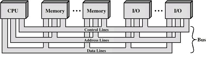
7 Bus 7
8 Buses There are a number of possible interconnection systems Single and multiple BUS structures are most common A Bus is a communication pathway connecting two or more devices Usually broadcast Often grouped A number of channels in one bus e.g. 32 bit data bus is 32 separate single bit channels Power lines may not be shown 8
9 Buses Data Bus Data Bus - Carries data there is no difference between data and instruction Width is a key determinant of performance (8, 16, 32, 64 bit) Address Bus - Identify the source or destination of data e.g. CPU needs to read an instruction (data) from a given location in memory Bus width determines maximum memory capacity of system Control Bus - Control and timing information Memory read/write signal Interrupt request Clock signals 9
10 Bus Interconnection Scheme 10

11 Physical Realization of Bus Architecture 11
12 Single Bus Problems Lots of devices on one bus leads to: Propagation delays Co-ordination of bus use can affect performance (long data paths) If aggregate data transfer approaches bus capacity Most systems use multiple buses to overcome these problems 12
13 High Performance Bus 13
14 Memory Hierarchy

15 Memory Hierarchy Registers In CPU Internal or Main memory More levels of cache RAM External memory Backing store 15
16 Characteristics Location CPU Internal External Capacity Word size Number of words Unit of transfer Internal: Usually governed by data bus width External: Usually a block which is much larger than a word Addressable unit: Smallest location uniquely addressed 16
17 Characteristics Access method Sequential (e.g. tape) Start at the beginning and read through in order Access time depends on location of data and previous location Direct (e.g. disk) Individual blocks have unique address Access is by jumping to vicinity plus sequential search Access time depends on location and previous location 17
18 Characteristics Access method Random (e.g. RAM) Individual addresses identify locations exactly Access time is independent of location or previous access Associative Data is located by a comparison with contents of a portion of the store Access time is independent of location or previous access 18
19 Characteristics Performance Access time Time between presenting the address and getting the valid data Memory Cycle time Time may be required for the memory to recover before next access Cycle time is access + recovery Transfer Rate Rate at which data can be moved 19
20 Characteristics Physical type Semiconductor (RAM) Magnetic (Disk & Tape) Optical (CD & DVD) Physical characteristics Decay Volatility Erasable Power consumption Organisation Physical arrangement of bits into words Not always obvious (e.g. interleaved) 20
21 Hierarchy List Registers L1 Cache L2 Cache L3 Cache Main memory Disk cache Disk Optical Tape 21
22 Cache Memory
23 Cache Small amount of fast memory Sits between normal main memory and CPU May be located on CPU chip or module 23

24 Cache and Main Memory 24

25 Cache/Main Memory Structure 25

26 Cache operation overview CPU requests contents of memory location Check cache for this data If present: get from cache else read required block from main memory to cache Then deliver to CPU Cache includes tags to identify which block of main memory is in each cache slot 26
27 Cache Design Addressing Size Mapping Function Replacement Algorithm Write Policy Block Size Number of Caches 27
28 Cache Addressing Where does cache sit? Between processor and virtual MMU Between MMU and main memory Logical cache (virtual cache) stores data using virtual addresses Processor accesses cache directly, not thorough physical cache Cache access faster, before MMU address translation Virtual addresses use same address space for different applications Must flush cache on each context switch Physical cache stores data using main memory physical addresses Logical address Physical address Processor Cache MMU Cache Main memory Data 28
29 Size does matter Cost More cache is expensive Speed More cache is faster (up to a point) Checking cache for data takes time 29
30 Direct Mapping Each block of main memory maps to only one cache line i.e. if a block is in cache, it must be in one specific place Address is in two parts Least Significant w bits identify unique word Most Significant s bits specify one memory block The MSBs are split into a cache line field r and a tag of s-r (most significant) Tag s-r Line or Slot r Word w

31 Direct Mapping from Cache to Main Memory 31
32 Direct Mapping Cache Organization 32
33 Direct Mapping pros & cons Simple Inexpensive Fixed location for given block If a program accesses 2 blocks that map to the same line repeatedly, cache misses are very high 33
34 Associative Mapping A main memory block can load into any line of cache Memory address is interpreted as tag and word Tag uniquely identifies block of memory Every line s tag is examined for a match Cache searching gets expensive Tag 22 bit Word 2 bit 34

35 Associative Mapping from Cache to Main Memory 35
36 Fully Associative Cache Organization 36
37 Associative Mapping Address Structure Tag 22 bit Word 2 bit 22 bit tag stored with each 32 bit block of data Compare tag field with tag entry in cache to check for hit Least significant 2 bits of address identify which 16 bit word is required from 32 bit data block e.g. Address Tag Data Cache line FFFFFC FFFFFC FFF 37
38 Associative Mapping Summary Address length = (s + w) bits Number of addressable units = 2 s+w words or bytes Block size = line size = 2 w words or bytes Number of blocks in main memory = 2 s+w /2 w = 2 s Number of lines in cache = undetermined Size of tag = s bits 38
39 Set Associative Mapping Cache is divided into a number of sets Each set contains a number of lines A given block maps to any line in a given set e.g. Block B can be in any line of set i e.g. 2 lines per set 2 way associative mapping A given block can be in one of 2 lines in only one set 39

40 Mapping From Main Memory to Cache: v Associative 40

41 Mapping From Main Memory to Cache: k-way Associative 41
42 K-Way Set Associative Cache Organization 42
43 Set Associative Mapping Address Structure Tag 9 bit Set 13 bit Word 2 bit Use set field to determine cache set to look in Compare tag field to see if we have a hit e.g Address Tag Data Set number 1FF 7FFC 1FF FFF 001 7FFC FFF 43
44 Set Associative Mapping Summary Address length = (s + w) bits Number of addressable units = 2 s+w words or bytes Block size = line size = 2 w words or bytes Number of blocks in main memory = 2 d Number of lines in set = k Number of sets = v = 2 d Number of lines in cache = kv = k * 2d Size of tag = (s d) bits 44
45 Replacement Algorithms Direct mapping No choice Each block only maps to one line Replace that line Associative & Set Associative Hardware implemented algorithm (speed) Least Recently used (LRU) but in 2 way set associative Which of the 2 block is lru? First in first out (FIFO) Least frequently used replace block which has had fewest hits Random 45
46 Write Policy Not overwrite a cache block if main memory is up to date I/O may address main memory directly Write through All writes go to main memory as well as cache Lots of traffic Slows down writes Write back Updates initially made in cache only and update bit is set If block is to be replaced, write to main memory only if update bit is set Other caches get out of sync I/O must access main memory through cache 46
47 Line Size Retrieve not only desired word but a number of adjacent words as well Increased block size will increase hit ratio at first the principle of locality Hit ratio will decreases as block becomes even bigger Probability of using newly fetched information becomes less than probability of reusing replaced Larger blocks Reduce number of blocks that fit in cache Data overwritten shortly after being fetched Each additional word is less local so less likely to be needed No definitive optimum value has been found 8 to 64 bytes seems reasonable For HPC systems, 64 and 128 byte most common 47
48 Multilevel Caches High logic density enables caches on chip Faster than bus access Frees bus for other transfers Common to use both on and off chip cache L1 on chip, L2 off chip in static RAM L2 access much faster than DRAM or ROM L2 often uses separate data path L2 may now be on chip Resulting in L3 cache Bus access or now on chip 48
49 Unified v Split Caches One cache for data and instructions or two, one for data and one for instructions Advantages of unified cache Higher hit rate Balances load of instruction and data fetch Only one cache to design & implement Advantages of split cache Eliminates cache contention between instruction fetch/decode unit and execution unit Important in pipelining 49
50 Internal Memory
51 Semiconductor Memory Types Memory Type Category Erasure Write Mechanism Volatility Random-access memory (RAM) Read-write memory Electrically, bytelevel Electrically Volatile Read-only memory (ROM) Programmable ROM (PROM) Read-only memory Not possible Masks Erasable PROM (EPROM) UV light, chiplevel Nonvolatile Electrically Erasable PROM (EEPROM) Read-mostly memory Electrically, bytelevel Electrically Flash memory Electrically, blocklevel 51
52 Semiconductor Memory RAM Misnamed as all semiconductor memory is random access Read/Write Volatile Temporary storage Static or dynamic 52
53 Memory Cell Operation 53
54 Dynamic RAM Bits stored as charge in capacitors Charges leak Need refreshing even when powered Simpler construction Smaller per bit Less expensive Need refresh circuits Slower Main memory Essentially analog Level of charge determines value 54
55 Static RAM Bits stored as on/off switches No charges to leak No refreshing needed when powered More complex construction Larger per bit More expensive Does not need refresh circuits Faster Cache Digital Uses flip-flops 55
56 SRAM v DRAM Both volatile Power needed to preserve data Dynamic cell Simpler to build, smaller More dense Less expensive Needs refresh Larger memory units Static Faster Cache 56
57 Read Only Memory (ROM) Permanent storage Nonvolatile Microprogramming Library subroutines Systems programs (BIOS) Function tables 57
58 Types of ROM Written during manufacture Very expensive for small runs Programmable (once) PROM Needs special equipment to program Read mostly Erasable Programmable (EPROM) Erased by UV Electrically Erasable (EEPROM) Takes much longer to write than read Flash memory Erase whole memory electrically 58
59 Organisation A 16Mbit chip can be organised as 1M of 16 bit words A bit per chip system has 16 lots of 1Mbit chip with bit 1 of each word in chip 1 and so on A 16Mbit chip can be organised as a 2048 x 2048 x 4bit array Reduces number of address pins Multiplex row address and column address 11 pins to address (2 11 =2048) Adding one more pin doubles range of values so x4 capacity 59
")
60 Typical 16 Mb DRAM (4M x 4) 60
61 256kByte Module Organisation 61
62 1MByte Module Organisation 62
63 Interleaved Memory Main memory is composed of a collection of DRAM memory chips that can be grouped together to form a memory bank It is possible to organize the memory banks in a way known as interleaved memory. Each bank is independently able to service a memory read or write request, so that a system with K banks can service K requests simultaneously, increasing memory read or write rates by a factor of K. If consecutive words of memory are stored in different banks, then the transfer of a block of memory is speeded up 63
64 Advanced DRAM Organization Basic DRAM same since first RAM chips Enhanced DRAM Contains small SRAM as well SRAM holds last line read (c.f. Cache!) Cache DRAM Larger SRAM component Use as cache or serial buffer 64
65 Synchronous DRAM (SDRAM) Access is synchronized with an external clock Address is presented to RAM RAM finds data (CPU waits in conventional DRAM) Since SDRAM moves data in time with system clock, CPU knows when data will be ready CPU does not have to wait, it can do something else Burst mode allows SDRAM to set up stream of data and fire it out in block DDR-SDRAM sends data twice per clock cycle (leading & trailing edge) 65

66 SDRAM 66
67 DDR SDRAM SDRAM can only send data once per clock Double-data-rate SDRAM can send data twice per clock cycle Rising edge and falling edge 67
68 External Memory
69 Types of External Memory Magnetic Disk RAID Removable Optical CD-ROM CD-Recordable (CD-R) CD-R/W DVD Magnetic Tape 69
70 Magnetic Disk Disk substrate coated with magnetizable material Substrate used to be aluminium Now glass Improved surface uniformity Increases reliability Reduction in surface defects Reduced read/write errors Lower flight heights (See later) Better stiffness Better shock/damage resistance 70
71 Read and Write Mechanisms Recording & retrieval via conductive coil called a head May be single read/write head or separate ones During read/write, head is stationary, platter rotates Write Current through coil produces magnetic field Pulses sent to head Magnetic pattern recorded on surface below Higher storage density and speed 71
72 Read and Write Mechanisms Read (traditional) Magnetic field moving relative to coil produces current Coil is the same for read and write Read (contemporary) Separate read head, close to write head Partially shielded magneto resistive (MR) sensor Electrical resistance depends on direction of magnetic field High frequency operation Higher storage density and speed 72
 Constant angular velocity Tracks divided into sectors Minimum block size is one sector May have more than one sector per")
73 Data Organization and Formatting Concentric rings or tracks Gaps between tracks Reduce gap to increase capacity Same number of bits per track (variable packing density) Constant angular velocity Tracks divided into sectors Minimum block size is one sector May have more than one sector per block 73
74 Disk Velocity Bit near centre of rotating disk passes fixed point slower than bit on outside of disk Increase spacing between bits in different tracks Rotate disk at constant angular velocity (CAV) Gives pie shaped sectors and concentric tracks Individual tracks and sectors addressable Move head to given track and wait for given sector Waste of space on outer tracks Lower data density Can use zones to increase capacity Each zone has fixed bits per track More complex circuitry 74

75 Disk Layout Methods Diagram 75
76 Finding Sectors Must be able to identify start of track and sector Format disk Additional information not available to user Marks tracks and sectors 76
77 Characteristics Fixed (rare) or movable head Removable or fixed Single or double (usually) sided Single or multiple platter Head mechanism Contact (Floppy) Fixed gap Flying (Winchester) 77
78 Fixed/Movable Head Disk Fixed head One read write head per track Heads mounted on fixed ridged arm Movable head One read write head per side Mounted on a movable arm 78
79 Removable or Not Removable disk Can be removed from drive and replaced with another disk Provides unlimited storage capacity Easy data transfer between systems Nonremovable disk Permanently mounted in the drive 79
")
80 Multiple Platter One head per side Heads are joined and aligned Aligned tracks on each platter form cylinders Data is striped by cylinder reduces head movement Increases speed (transfer rate) 80
81 Winchester Hard Disk Developed by IBM in Winchester (USA) Sealed unit One or more platters (disks) Heads fly on boundary layer of air as disk spins Very small head to disk gap Getting more robust Universal Cheap Fastest external storage Getting larger all the time 250 Gigabyte now easily available 81
82 Speed Seek time Moving head to correct track (Rotational) latency Waiting for data to rotate under head Access time = Seek + Latency Transfer rate 82
83 RAID Redundant Array of Independent Disks Redundant Array of Inexpensive Disks 6 levels in common use Not a hierarchy Set of physical disks viewed as single logical drive by O/S Data distributed across physical drives Can use redundant capacity to store parity information 83
84 RAID 0 RAID 0 No redundancy Data striped across all disks Round Robin striping Increase speed Multiple data requests probably not on same disk Disks seek in parallel A set of data is likely to be striped across multiple disks RAID 1 Mirrored Disks Data is striped across disks 2 copies of each stripe on separate disks Read from either Write to both Recovery is simple Swap faulty disk & re-mirror No down time Expensive 84
85 RAID RAID 2 Disks are synchronized Very small stripes Often single byte/word Error correction calculated across corresponding bits on disks Multiple parity disks store Hamming code error Lots of redundancy (expensive) 85 RAID 3 Similar to RAID 2 Only one redundant disk, no matter how large the array Simple parity bit for each set of corresponding bits Data on failed drive can be reconstructed from surviving data and parity info Very high transfer rates
86 RAID RAID 4 Each disk operates independently Good for high I/O request rate Large stripes Bit by bit parity calculated across stripes on each disk Parity stored on parity disk 86 RAID 5 Like RAID 4 Parity striped across all disks Round robin allocation for parity stripe Avoids RAID 4 bottleneck at parity disk Commonly used in network servers RAID 6 Two parity calculations Stored in separate blocks on different disks User requirement of N disks needs N+2 High data availability Three disks need to fail for data loss Significant write penalty

87 RAID 0, 1, 2 87

88 RAID 3 & 4 88

89 RAID 5 & 6 89
90 Optical Storage CD-ROM Originally for audio 650Mbytes giving over 70 minutes audio Polycarbonate coated with highly reflective coat, usually aluminium Data stored as pits Read by reflecting laser Constant packing density Constant linear velocity 90

91 CD Operation 91
92 CD-ROM Drive Speeds Audio is single speed Constant linier velocity 1.2 ms -1 Track (spiral) is 5.27km long Gives 4391 seconds = 73.2 minutes Other speeds are quoted as multiples e.g. 24x Quoted figure is maximum drive can achieve 92

93 CD-ROM Format Mode 0=blank data field Mode 1=2048 byte data+error correction Mode 2=2336 byte data 93
94 Random Access on CD-ROM Difficult Move head to rough position Set correct speed Read address Adjust to required location (Yawn!) 94
95 CD-ROM for & against Large capacity (?) Easy to mass produce Removable Robust Expensive for small runs Slow Read only 95
96 Other Optical Storage CD-Recordable (CD-R) WORM Now affordable Compatible with CD-ROM drives CD-RW Erasable Getting cheaper Mostly CD-ROM drive compatible Phase change Material has two different reflectivities in different phase states 96
97 DVD - what s in a name? Digital Video Disk Used to indicate a player for movies Only plays video disks Digital Versatile Disk Used to indicate a computer drive Will read computer disks and play video disks 97
98 DVD - technology Multi-layer Very high capacity (4.7G per layer) Full length movie on single disk Using MPEG compression Finally standardized Movies carry regional coding Players only play correct region films Can be fixed 98
99 High Definition Optical Disks Designed for high definition videos Much higher capacity than DVD Shorter wavelength laser Blue-violet range Smaller pits HD-DVD 15GB single side single layer Blue-ray Data layer closer to laser Tighter focus, less distortion, smaller pits 25GB on single layer Available read only (BD-ROM), Recordable once (BR-R) and rerecordable (BR-RE) 99

100 Optical Memory Characteristics 100
101 Magnetic Tape Serial access Slow Very cheap Backup and archive Linear Tape-Open (LTO) Tape Drives Developed late 1990s Open source alternative to proprietary tape systems 101
102 Input Output
103 Input/Output Problems Input/Output Problems Wide variety of peripherals Delivering different amounts of data At different speeds In different formats All slower than CPU and RAM Need I/O modules Input/Output module Interface to CPU and Memory Interface to one or more peripherals 103

104 Generic Model of I/O Module 104
105 External Devices Human readable Screen, printer, keyboard Machine readable Monitoring and control Communication Modem Network Interface Card (NIC) 105

106 External Device Block Diagram 106
107 I/O Module Function Control & Timing CPU Communication Device Communication Data Buffering Error Detection 107
108 I/O Steps CPU checks I/O module device status I/O module returns status If ready, CPU requests data transfer I/O module gets data from device I/O module transfers data to CPU Variations for output, DMA, etc. 108

109 I/O Module Diagram 109
110 I/O Module Decisions Hide or reveal device properties to CPU Support multiple or single device Control device functions or leave for CPU Also O/S decisions e.g. Unix treats everything it can as a file 110
111 Input Output Techniques Programmed Interrupt driven Direct Memory Access (DMA) 111

112 Three Techniques for Input of a Block of Data 112
113 Programmed I/O CPU has direct control over I/O Sensing status Read/write commands Transferring data CPU waits for I/O module to complete operation Wastes CPU time 113
114 Programmed I/O - detail CPU requests I/O operation I/O module performs operation I/O module sets status bits CPU checks status bits periodically I/O module does not inform CPU directly I/O module does not interrupt CPU CPU may wait or come back later 114
115 I/O Commands CPU issues address Identifies module (& device if >1 per module) CPU issues command Control - telling module what to do e.g. spin up disk Test - check status e.g. power? Error? Read/Write Module transfers data via buffer from/to device 115
116 Addressing I/O Devices Under programmed I/O data transfer is very like memory access (CPU viewpoint) Each device given unique identifier CPU commands contain identifier (address) 116
117 I/O Mapping Memory mapped I/O Devices and memory share an address space I/O looks just like memory read/write No special commands for I/O Large selection of memory access commands available Isolated I/O Separate address spaces Need I/O or memory select lines Special commands for I/O Limited set 117
118 Interrupt Driven I/O Overcomes CPU waiting No repeated CPU checking of device I/O module interrupts when ready 118
119 Interrupt Driven I/O - Basic Operation CPU issues read command I/O module gets data from peripheral whilst CPU does other work I/O module interrupts CPU CPU requests data I/O module transfers data 119

120 Simple Interrupt Processing 120
121 CPU Viewpoint Issue read command Do other work Check for interrupt at end of each instruction cycle If interrupted:- Save context (registers) Process interrupt Fetch data & store See Operating Systems notes 121

122 Changes in Memory and Registers for an Interrupt 122
123 Design Issues How do you identify the module issuing the interrupt? How do you deal with multiple interrupts? i.e. an interrupt handler being interrupted 123
124 Identifying Interrupting Module Different line for each module PC Limits number of devices Software poll CPU asks each module in turn Slow 124
125 Identifying Interrupting Module Daisy Chain or Hardware poll Interrupt Acknowledge sent down a chain Module responsible places vector on bus CPU uses vector to identify handler routine Bus Master Module must claim the bus before it can raise interrupt e.g. PCI & SCSI 125
126 Multiple Interrupts Each interrupt line has a priority Higher priority lines can interrupt lower priority lines If bus mastering only current master can interrupt 126
127 Direct Memory Access Interrupt driven and programmed I/O require active CPU intervention Transfer rate is limited CPU is tied up DMA is the answer Additional Module (hardware) on bus DMA controller takes over from CPU for I/O 127

128 Typical DMA Module Diagram 128
129 DMA Operation CPU tells DMA controller: Read/Write Device address Starting address of memory block for data Amount of data to be transferred CPU carries on with other work DMA controller deals with transfer DMA controller sends interrupt when finished 129
130 DMA Transfer - Cycle Stealing DMA controller takes over bus for a cycle Transfer of one word of data Not an interrupt CPU does not switch context CPU suspended just before it accesses bus i.e. before an operand or data fetch or a data write Slows down CPU but not as much as CPU doing transfer 130
131 DMA and Interrupt Breakpoints During an Instruction Cycle 131
132 DMA Configurations (1) Single Bus, Detached DMA controller Each transfer uses bus twice I/O to DMA then DMA to memory CPU is suspended twice 132

133 DMA Configurations (2) Single Bus, Integrated DMA controller Controller may support >1 device Each transfer uses bus once DMA to memory CPU is suspended once 133

134 DMA Configurations (3) Separate I/O Bus Bus supports all DMA enabled devices Each transfer uses bus once DMA to memory CPU is suspended once 134
135 I/O Channels I/O devices getting more sophisticated e.g. 3D graphics cards CPU instructs I/O controller to do transfer I/O controller does entire transfer Improves speed Takes load off CPU Dedicated processor is faster 135


136 I/O Channel Architecture 136
137 Interfacing Connecting devices together Bit of wire? Dedicated processor/memory/buses? E.g. FireWire, InfiniBand 137
138 IEEE 1394 FireWire High performance serial bus Fast Low cost Easy to implement Also being used in digital cameras, VCRs and TV 138
139 FireWire Configuration Daisy chain Up to 63 devices on single port Really 64 of which one is the interface itself Up to 1022 buses can be connected with bridges Automatic configuration No bus terminators May be tree structure 139

140 Simple FireWire Configuration 140
141 InfiniBand I/O specification aimed at high end servers Merger of Future I/O (Cisco, HP, Compaq, IBM) and Next Generation I/O (Intel) Version 1 released early 2001 Architecture and spec. for data flow between processor and intelligent I/O devices Intended to replace PCI in servers Increased capacity, expandability, flexibility 141
142 InfiniBand Architecture Remote storage, networking and connection between servers Attach servers, remote storage, network devices to central fabric of switches and links Greater server density Scalable data centre Independent nodes added as required I/O distance from server up to 17m using copper 300m multimode fibre optic 10km single mode fibre Up to 30Gbps 142

143 InfiniBand Switch Fabric 143
144 InfiniBand Operation 16 logical channels (virtual lanes) per physical link One lane for management, rest for data Data in stream of packets Virtual lane dedicated temporarily to end to end transfer Switch maps traffic from incoming to outgoing lane 144
Advanced Parallel Architecture Lesson 4 bis. Annalisa Massini /2015
 Advanced Parallel Architecture Lesson 4 bis Annalisa Massini - 2014/2015 Internal Memory RAM Many memory types are random access individual words of memory are directly accessed through wired-in addressing
Semiconductor Memory Types Microprocessor Design & Organisation HCA2102
 Semiconductor Memory Types Microprocessor Design & Organisation HCA2102 Internal & External Memory Semiconductor Memory RAM Misnamed as all semiconductor memory is random access Read/Write Volatile Temporary
William Stallings Computer Organization and Architecture 8 th Edition. Chapter 6 External Memory
 William Stallings Computer Organization and Architecture 8 th Edition Chapter 6 External Memory Types of External Memory Magnetic Disk RAID Removable Optical CD-ROM CD-Recordable (CD-R) CD-R/W DVD Magnetic
William Stallings Computer Organization and Architecture 6 th Edition. Chapter 6 External Memory
 William Stallings Computer Organization and Architecture 6 th Edition Chapter 6 External Memory Types of External Memory Magnetic Disk RAID Removable Optical CD-ROM CD-Recordable (CD-R) CD-R/W DVD Magnetic
Magnetic Disk. Optical. Magnetic Tape. RAID Removable. CD-ROM CD-Recordable (CD-R) CD-R/W DVD
 CD-R/W DVD") External Memory Magnetic Disk RAID Removable Optical CD-ROM CD-Recordable (CD-R) CD-R/W DVD Magnetic Tape Disk substrate coated with magnetizable material (iron oxide rust) Substrate used to be aluminium
External Memory Magnetic Disk RAID Removable Optical CD-ROM CD-Recordable (CD-R) CD-R/W DVD Magnetic Tape Disk substrate coated with magnetizable material (iron oxide rust) Substrate used to be aluminium
Semiconductor Memory Types. Computer & Microprocessor Architecture HCA103. Memory Cell Operation. Semiconductor Memory.
 Semiconductor Memory Types Computer & Microprocessor Architecture HCA103 Internal & External Memory UTM-RHH Slide Set 5 1 UTM-RHH Slide Set 5 2 Semiconductor Memory RAM Misnamed as all semiconductor memory
Chapter 6 External Memory
 Chapter 6 External Memory Magnetic Disk Removable RAID Disk substrate coated with magnetizable material (iron oxide rust) Substrate used to be aluminium Now glass Improved surface uniformity Increases
Chapter 4 Main Memory
 Chapter 4 Main Memory Course Outcome (CO) - CO2 Describe the architecture and organization of computer systems Program Outcome (PO) PO1 Apply knowledge of mathematics, science and engineering fundamentals
External Memory. Computer Architecture. Magnetic Disk. Outline. Data Organization and Formatting. Write and Read Mechanisms
 Computer Architecture Prof. Dr. Nizamettin AYDIN naydin@yildiz.edu.tr nizamettinaydin@gmail.com External Memory http://www.yildiz.edu.tr/~naydin 1 2 Outline Types of External Memory Magnetic Disk Magnetic
Contents. Memory System Overview Cache Memory. Internal Memory. Virtual Memory. Memory Hierarchy. Registers In CPU Internal or Main memory
 Memory Hierarchy Contents Memory System Overview Cache Memory Internal Memory External Memory Virtual Memory Memory Hierarchy Registers In CPU Internal or Main memory Cache RAM External memory Backing
External Memory. Types of External Memory. Magnetic Disk. Optical. Magnetic Tape. RAID Removable. CD-ROM CD-Recordable (CD-R) CD-R/W DVD
 CD-R/W DVD") External Memory 1 Types of External Memory Magnetic Disk RAID Removable Optical CD-ROM CD-Recordable (CD-R) CD-R/W DVD Magnetic Tape 2 1 3 Magnetic Disk Disk substrate coated with magnetizable material
External Memory 1 Types of External Memory Magnetic Disk RAID Removable Optical CD-ROM CD-Recordable (CD-R) CD-R/W DVD Magnetic Tape 2 1 3 Magnetic Disk Disk substrate coated with magnetizable material
Memory and Disk Systems
 COMP 212 Computer Organization & Architecture Re-Cap of Lecture #3 Cache system is a compromise between COMP 212 Fall 2008 Lecture 4 Memory and Disk Systems More memory system capacity Faster access speed
Generic Model of I/O Module Interface to CPU and Memory Interface to one or more peripherals
 William Stallings Computer Organization and Architecture 7 th Edition Chapter 7 Input/Output Input/Output Problems Wide variety of peripherals Delivering different amounts of data At different speeds In
William Stallings Computer Organization and Architecture 8th Edition. Cache Memory
 William Stallings Computer Organization and Architecture 8th Edition Chapter 4 Cache Memory Characteristics Location Capacity Unit of transfer Access method Performance Physical type Physical characteristics
Unit 2. Chapter 4 Cache Memory
 Unit 2 Chapter 4 Cache Memory Characteristics Location Capacity Unit of transfer Access method Performance Physical type Physical characteristics Organisation Location CPU Internal External Capacity Word
William Stallings Computer Organization and Architecture 6th Edition. Chapter 5 Internal Memory
 William Stallings Computer Organization and Architecture 6th Edition Chapter 5 Internal Memory Semiconductor Memory Types Semiconductor Memory RAM Misnamed as all semiconductor memory is random access
Computer Organization. 8th Edition. Chapter 5 Internal Memory
 William Stallings Computer Organization and Architecture 8th Edition Chapter 5 Internal Memory Semiconductor Memory Types Memory Type Category Erasure Write Mechanism Volatility Random-access memory (RAM)
Chapter 5 Internal Memory
 Chapter 5 Internal Memory Memory Type Category Erasure Write Mechanism Volatility Random-access memory (RAM) Read-write memory Electrically, byte-level Electrically Volatile Read-only memory (ROM) Read-only
Overview IN this chapter we will study. William Stallings Computer Organization and Architecture 6th Edition
 William Stallings Computer Organization and Architecture 6th Edition Chapter 4 Cache Memory Overview IN this chapter we will study 4.1 COMPUTER MEMORY SYSTEM OVERVIEW 4.2 CACHE MEMORY PRINCIPLES 4.3 ELEMENTS
Organization. 5.1 Semiconductor Main Memory. William Stallings Computer Organization and Architecture 6th Edition
 William Stallings Computer Organization and Architecture 6th Edition Chapter 5 Internal Memory 5.1 Semiconductor Main Memory 5.2 Error Correction 5.3 Advanced DRAM Organization 5.1 Semiconductor Main Memory
Computer & Microprocessor Architecture HCA103
 Computer & Microprocessor Architecture HCA103 Cache Memory UTM-RHH Slide Set 4 1 Characteristics Location Capacity Unit of transfer Access method Performance Physical type Physical characteristics Organisation
Internal Memory. Computer Architecture. Outline. Memory Hierarchy. Semiconductor Memory Types. Copyright 2000 N. AYDIN. All rights reserved.
 Computer Architecture Prof. Dr. Nizamettin AYDIN naydin@yildiz.edu.tr nizamettinaydin@gmail.com Internal Memory http://www.yildiz.edu.tr/~naydin 1 2 Outline Semiconductor main memory Random Access Memory
Input/Output Problems. External Devices. Input/Output Module. I/O Steps. I/O Module Function Computer Architecture
 168 420 Computer Architecture Chapter 6 Input/Output Input/Output Problems Wide variety of peripherals Delivering different amounts of data At different speeds In different formats All slower than CPU
BCN1043. By Dr. Mritha Ramalingam. Faculty of Computer Systems & Software Engineering
 BCN1043 By Dr. Mritha Ramalingam Faculty of Computer Systems & Software Engineering mritha@ump.edu.my http://ocw.ump.edu.my/ authors Dr. Mohd Nizam Mohmad Kahar (mnizam@ump.edu.my) Jamaludin Sallim (jamal@ump.edu.my)
COSC 243. Memory and Storage Systems. Lecture 10 Memory and Storage Systems. COSC 243 (Computer Architecture)
") COSC 243 1 Overview This Lecture Source: Chapters 4, 5, and 6 (10 th edition) Next Lecture Control Unit and Microprogramming 2 Electromagnetic Induction Move a magnet through a coil to induce a current
COSC 243 1 Overview This Lecture Source: Chapters 4, 5, and 6 (10 th edition) Next Lecture Control Unit and Microprogramming 2 Electromagnetic Induction Move a magnet through a coil to induce a current
Characteristics. Microprocessor Design & Organisation HCA2102. Unit of Transfer. Location. Memory Hierarchy Diagram
 Microprocessor Design & Organisation HCA2102 Cache Memory Characteristics Location Unit of transfer Access method Performance Physical type Physical Characteristics UTM-RHH Slide Set 5 2 Location Internal
Computer Organization ECE514. Chapter 5 Input/Output (9hrs)
") Computer Organization ECE514 Chapter 5 Input/Output (9hrs) Learning Outcomes Course Outcome (CO) - CO2 Describe the architecture and organization of computer systems Program Outcome (PO) PO1 Apply knowledge
Computer Organization ECE514 Chapter 5 Input/Output (9hrs) Learning Outcomes Course Outcome (CO) - CO2 Describe the architecture and organization of computer systems Program Outcome (PO) PO1 Apply knowledge
Characteristics of Memory Location wrt Motherboard. CSCI 4717 Computer Architecture. Characteristics of Memory Capacity Addressable Units
 CSCI 4717/5717 Computer Architecture Topic: Cache Memory Reading: Stallings, Chapter 4 Characteristics of Memory Location wrt Motherboard Inside CPU temporary memory or registers Motherboard main memory
Memory Pearson Education, Inc., Hoboken, NJ. All rights reserved.
 1 Memory + 2 Location Internal (e.g. processor registers, cache, main memory) External (e.g. optical disks, magnetic disks, tapes) Capacity Number of words Number of bytes Unit of Transfer Word Block Access
Organisasi Sistem Komputer
 LOGO Organisasi Sistem Komputer OSK 5 Input Output 1 1 PT. Elektronika FT UNY Input/Output Problems Wide variety of peripherals Delivering different amounts of data At different speeds In different formats
Chapter 5. Internal Memory. Yonsei University
 Chapter 5 Internal Memory Contents Main Memory Error Correction Advanced DRAM Organization 5-2 Memory Types Memory Type Category Erasure Write Mechanism Volatility Random-access memory(ram) Read-write
Overview. EE 4504 Computer Organization. Historically, the limiting factor in a computer s performance has been memory access time
 Overview EE 4504 Computer Organization Section 3 Computer Memory Historically, the limiting factor in a computer s performance has been memory access time Memory speed has been slow compared to the speed
External Memory. Patrick Happ Raul Queiroz Feitosa. Parts of these slides are from the support material provided by W. Stallings
 External Memory Patrick Happ Raul Queiroz Feitosa Parts of these slides are from the support material provided by W. Stallings Objective This chapter examines a range of external memory devices and systems.
William Stallings Computer Organization and Architecture 8th Edition. Chapter 5 Internal Memory
 William Stallings Computer Organization and Architecture 8th Edition Chapter 5 Internal Memory Semiconductor Memory The basic element of a semiconductor memory is the memory cell. Although a variety of
Chapter 4. Cache Memory. Yonsei University
 Chapter 4 Cache Memory Contents Computer Memory System Overview Cache Memory Principles Elements of Cache Design Pentium 4 and Power PC Cache 4-2 Key Characteristics 4-3 Location Processor Internal (main)
UNIT-V MEMORY ORGANIZATION
 UNIT-V MEMORY ORGANIZATION 1 The main memory of a computer is semiconductor memory.the main memory unit is basically consists of two kinds of memory: RAM (RWM):Random access memory; which is volatile in
Computer Organization and Assembly Language (CS-506)
") Computer Organization and Assembly Language (CS-506) Muhammad Zeeshan Haider Ali Lecturer ISP. Multan ali.zeeshan04@gmail.com https://zeeshanaliatisp.wordpress.com/ Lecture 2 Memory Organization and Structure
Computer Organization and Assembly Language (CS-506) Muhammad Zeeshan Haider Ali Lecturer ISP. Multan ali.zeeshan04@gmail.com https://zeeshanaliatisp.wordpress.com/ Lecture 2 Memory Organization and Structure
Computer Organization
 INF 101 Fundamental Information Technology Computer Organization Assistant Prof. Dr. Turgay ĐBRĐKÇĐ Course slides are adapted from slides provided by Addison-Wesley Computing Fundamentals of Information
William Stallings Computer Organization and Architecture 10 th Edition Pearson Education, Inc., Hoboken, NJ. All rights reserved.
 + William Stallings Computer Organization and Architecture 10 th Edition 2016 Pearson Education, Inc., Hoboken, NJ. All rights reserved. 2 + Chapter 4 Cache Memory 3 Location Internal (e.g. processor registers,
k -bit address bus n-bit data bus Control lines ( R W, MFC, etc.)
") THE MEMORY SYSTEM SOME BASIC CONCEPTS Maximum size of the Main Memory byte-addressable CPU-Main Memory Connection, Processor MAR MDR k -bit address bus n-bit data bus Memory Up to 2 k addressable locations
THE MEMORY SYSTEM SOME BASIC CONCEPTS Maximum size of the Main Memory byte-addressable CPU-Main Memory Connection, Processor MAR MDR k -bit address bus n-bit data bus Memory Up to 2 k addressable locations
A track on a magnetic disk is a concentric rings where data is stored.
 CS 320 Ch 6 External Memory Figure 6.1 shows a typical read/ head on a magnetic disk system. Read and heads separate. Read head uses a material that changes resistance in response to a magnetic field.
(Advanced) Computer Organization & Architechture. Prof. Dr. Hasan Hüseyin BALIK (4 th Week)
 Computer Organization & Architechture. Prof. Dr. Hasan Hüseyin BALIK (4 th Week)") + (Advanced) Computer Organization & Architechture Prof. Dr. Hasan Hüseyin BALIK (4 th Week) + Outline 2. The computer system 2.1 A Top-Level View of Computer Function and Interconnection 2.2 Cache Memory
+ (Advanced) Computer Organization & Architechture Prof. Dr. Hasan Hüseyin BALIK (4 th Week) + Outline 2. The computer system 2.1 A Top-Level View of Computer Function and Interconnection 2.2 Cache Memory
Module 5a: Introduction To Memory System (MAIN MEMORY)
") Module 5a: Introduction To Memory System (MAIN MEMORY) R E F E R E N C E S : S T A L L I N G S, C O M P U T E R O R G A N I Z A T I O N A N D A R C H I T E C T U R E M O R R I S M A N O, C O M P U T E
Module 5a: Introduction To Memory System (MAIN MEMORY) R E F E R E N C E S : S T A L L I N G S, C O M P U T E R O R G A N I Z A T I O N A N D A R C H I T E C T U R E M O R R I S M A N O, C O M P U T E
WEEK 7. Chapter 4. Cache Memory Pearson Education, Inc., Hoboken, NJ. All rights reserved.
 WEEK 7 + Chapter 4 Cache Memory Location Internal (e.g. processor registers, cache, main memory) External (e.g. optical disks, magnetic disks, tapes) Capacity Number of words Number of bytes Unit of Transfer
5 Computer Organization
 5 Computer Organization 5.1 Foundations of Computer Science ã Cengage Learning Objectives After studying this chapter, the student should be able to: q List the three subsystems of a computer. q Describe
1.1 Bits and Bit Patterns. Boolean Operations. Figure 2.1 CPU and main memory connected via a bus. CS11102 Introduction to Computer Science
 1.1 Bits and Bit Patterns CS11102 Introduction to Computer Science Data Storage 1.1 Bits and Their Storage 1.2 Main Memory 1.3 Mass Storage 1.4 Representation of information as bit patterns Bit: Binary
Basic Organization Memory Cell Operation. CSCI 4717 Computer Architecture. ROM Uses. Random Access Memory. Semiconductor Memory Types
 CSCI 4717/5717 Computer Architecture Topic: Internal Memory Details Reading: Stallings, Sections 5.1 & 5.3 Basic Organization Memory Cell Operation Represent two stable/semi-stable states representing
EXTERNAL MEMORY (Part 1)
") Eastern Mediterranean University School of Computing and Technology ITEC255 Computer Organization & Architecture EXTERNAL MEMORY (Part 1) Introduction When external memory is discussed, one should consider
Eastern Mediterranean University School of Computing and Technology ITEC255 Computer Organization & Architecture EXTERNAL MEMORY (Part 1) Introduction When external memory is discussed, one should consider
Eastern Mediterranean University School of Computing and Technology CACHE MEMORY. Computer memory is organized into a hierarchy.
 Eastern Mediterranean University School of Computing and Technology ITEC255 Computer Organization & Architecture CACHE MEMORY Introduction Computer memory is organized into a hierarchy. At the highest
Computer Organization and Structure. Bing-Yu Chen National Taiwan University
 Computer Organization and Structure Bing-Yu Chen National Taiwan University Storage and Other I/O Topics I/O Performance Measures Types and Characteristics of I/O Devices Buses Interfacing I/O Devices
Computer Organization and Technology External Memory
 Computer Organization and Technology External Memory Assoc. Prof. Dr. Wattanapong Kurdthongmee Division of Computer Engineering, School of Engineering and Resources, Walailak University 1 Magnetic Disk
COMPUTER ARCHITECTURE AND ORGANIZATION
 Memory System 1. Microcomputer Memory Memory is an essential component of the microcomputer system. It stores binary instructions and datum for the microcomputer. The memory is the place where the computer
UNIT 2 Data Center Environment
 UNIT 2 Data Center Environment This chapter provides an understanding of various logical components of hosts such as file systems, volume managers, and operating systems, and their role in the storage
CS 320 February 2, 2018 Ch 5 Memory
 CS 320 February 2, 2018 Ch 5 Memory Main memory often referred to as core by the older generation because core memory was a mainstay of computers until the advent of cheap semi-conductor memory in the
CS 261 Fall Mike Lam, Professor. Memory
 CS 261 Fall 2016 Mike Lam, Professor Memory Topics Memory hierarchy overview Storage technologies SRAM DRAM PROM / flash Disk storage Tape and network storage I/O architecture Storage trends Latency comparisons
Computer Organization
 Chapter 5 Computer Organization Figure 5-1 Computer hardware :: Review Figure 5-2 CPU :: Review CPU:: Review Registers are fast stand-alone storage locations that hold data temporarily Data Registers Instructional
PRATHYUSHA INSTITUTE OF TECHNOLOGY AND MANAGEMENT
 PRATHYUSHA INSTITUTE OF TECHNOLOGY AND MANAGEMENT DEPARTMENT OF INFORMATION TECHNOLOGY Staff Name: Prof. S. Athinarayanan UNIT IV PART A Branch: ECE / V Sem 1. Define Memory Access Time and Memory Cycle
Computers in Business: Concepts in Hardware and Software
 Computers in Business: Concepts in and Software University for Development Studies (UDS) January 31, 2012 NB: Listen to what I say, What matters is not what is in the notes. Assignments are very essential
Virtual Memory. Reading. Sections 5.4, 5.5, 5.6, 5.8, 5.10 (2) Lecture notes from MKP and S. Yalamanchili
 Lecture notes from MKP and S. Yalamanchili") Virtual Memory Lecture notes from MKP and S. Yalamanchili Sections 5.4, 5.5, 5.6, 5.8, 5.10 Reading (2) 1 The Memory Hierarchy ALU registers Cache Memory Memory Memory Managed by the compiler Memory Managed
Virtual Memory Lecture notes from MKP and S. Yalamanchili Sections 5.4, 5.5, 5.6, 5.8, 5.10 Reading (2) 1 The Memory Hierarchy ALU registers Cache Memory Memory Memory Managed by the compiler Memory Managed
SAE5C Computer Organization and Architecture. Unit : I - V
 SAE5C Computer Organization and Architecture Unit : I - V UNIT-I Evolution of Pentium and Power PC Evolution of Computer Components functions Interconnection Bus Basics of PCI Memory:Characteristics,Hierarchy
UC Santa Barbara. Operating Systems. Christopher Kruegel Department of Computer Science UC Santa Barbara
 Operating Systems Christopher Kruegel Department of Computer Science http://www.cs.ucsb.edu/~chris/ Input and Output Input/Output Devices The OS is responsible for managing I/O devices Issue requests Manage
Database Management Systems, 2nd edition, Raghu Ramakrishnan, Johannes Gehrke, McGraw-Hill
 Lecture Handout Database Management System Lecture No. 34 Reading Material Database Management Systems, 2nd edition, Raghu Ramakrishnan, Johannes Gehrke, McGraw-Hill Modern Database Management, Fred McFadden,
Storage Systems. Storage Systems
 Storage Systems Storage Systems We already know about four levels of storage: Registers Cache Memory Disk But we've been a little vague on how these devices are interconnected In this unit, we study Input/output
Memory Overview. Overview - Memory Types 2/17/16. Curtis Nelson Walla Walla University
 Memory Overview Curtis Nelson Walla Walla University Overview - Memory Types n n n Magnetic tape (used primarily for long term archive) Magnetic disk n Hard disk (File, Directory, Folder) n Floppy disks
Digital Design Laboratory Lecture 6 I/O
 ECE 280 / CSE 280 Digital Design Laboratory Lecture 6 I/O Input/Output Module Interface to CPU and Memory Interface to one or more peripherals Generic Model of I/O Module External Devices Human readable
CREATED BY M BILAL & Arslan Ahmad Shaad Visit:
 CREATED BY M BILAL & Arslan Ahmad Shaad Visit: www.techo786.wordpress.com Q1: Define microprocessor? Short Questions Chapter No 01 Fundamental Concepts Microprocessor is a program-controlled and semiconductor
I/O Management and Disk Scheduling. Chapter 11
 I/O Management and Disk Scheduling Chapter 11 Categories of I/O Devices Human readable used to communicate with the user video display terminals keyboard mouse printer Categories of I/O Devices Machine
Storage. Hwansoo Han
 Storage Hwansoo Han I/O Devices I/O devices can be characterized by Behavior: input, out, storage Partner: human or machine Data rate: bytes/sec, transfers/sec I/O bus connections 2 I/O System Characteristics
Input/Output. Today. Next. Principles of I/O hardware & software I/O software layers Disks. Protection & Security
 Input/Output Today Principles of I/O hardware & software I/O software layers Disks Next Protection & Security Operating Systems and I/O Two key operating system goals Control I/O devices Provide a simple,
CO212 Lecture 6: Memory Organization III
 CO212 Lecture 6: Memory Organization III Shobhanjana Kalita, Dept. of CSE, Tezpur University Slides courtesy: Computer Architecture and Organization, 9 th Ed, W. Stallings External Memory Magnetic disks
Mass-Storage Structure
 CS 4410 Operating Systems Mass-Storage Structure Summer 2011 Cornell University 1 Today How is data saved in the hard disk? Magnetic disk Disk speed parameters Disk Scheduling RAID Structure 2 Secondary
Embedded Systems Design: A Unified Hardware/Software Introduction. Outline. Chapter 5 Memory. Introduction. Memory: basic concepts
 Hardware/Software Introduction Chapter 5 Memory Outline Memory Write Ability and Storage Permanence Common Memory Types Composing Memory Memory Hierarchy and Cache Advanced RAM 1 2 Introduction Memory:
Embedded Systems Design: A Unified Hardware/Software Introduction. Chapter 5 Memory. Outline. Introduction
 Hardware/Software Introduction Chapter 5 Memory 1 Outline Memory Write Ability and Storage Permanence Common Memory Types Composing Memory Memory Hierarchy and Cache Advanced RAM 2 Introduction Embedded
(Advanced) Computer Organization & Architechture. Prof. Dr. Hasan Hüseyin BALIK (5 th Week)
 Computer Organization & Architechture. Prof. Dr. Hasan Hüseyin BALIK (5 th Week)") + (Advanced) Computer Organization & Architechture Prof. Dr. Hasan Hüseyin BALIK (5 th Week) + Outline 2. The computer system 2.1 A Top-Level View of Computer Function and Interconnection 2.2 Cache Memory
+ (Advanced) Computer Organization & Architechture Prof. Dr. Hasan Hüseyin BALIK (5 th Week) + Outline 2. The computer system 2.1 A Top-Level View of Computer Function and Interconnection 2.2 Cache Memory
Chapter One. Introduction to Computer System
 Principles of Programming-I / 131101 Prepared by: Dr. Bahjat Qazzaz -------------------------------------------------------------------------------------------- Chapter One Introduction to Computer System
Introduction Disks RAID Tertiary storage. Mass Storage. CMSC 420, York College. November 21, 2006
 November 21, 2006 The memory hierarchy Red = Level Access time Capacity Features Registers nanoseconds 100s of bytes fixed Cache nanoseconds 1-2 MB fixed RAM nanoseconds MBs to GBs expandable Disk milliseconds
CS 33. Memory Hierarchy I. CS33 Intro to Computer Systems XVI 1 Copyright 2016 Thomas W. Doeppner. All rights reserved.
 CS 33 Memory Hierarchy I CS33 Intro to Computer Systems XVI 1 Copyright 2016 Thomas W. Doeppner. All rights reserved. Random-Access Memory (RAM) Key features RAM is traditionally packaged as a chip basic
I/O CANNOT BE IGNORED
 LECTURE 13 I/O I/O CANNOT BE IGNORED Assume a program requires 100 seconds, 90 seconds for main memory, 10 seconds for I/O. Assume main memory access improves by ~10% per year and I/O remains the same.
TK2123: COMPUTER ORGANISATION & ARCHITECTURE. CPU and Memory (2)
") TK2123: COMPUTER ORGANISATION & ARCHITECTURE CPU and Memory (2) 1 Contents This lecture will discuss: Cache. Error Correcting Codes. 2 The Memory Hierarchy Trade-off: cost, capacity and access time. Faster
TK2123: COMPUTER ORGANISATION & ARCHITECTURE CPU and Memory (2) 1 Contents This lecture will discuss: Cache. Error Correcting Codes. 2 The Memory Hierarchy Trade-off: cost, capacity and access time. Faster
Computer Systems Organization
 The IAS (von Neumann) Machine Computer Systems Organization Input Output Equipment Stored Program concept Main memory storing programs and data ALU operating on binary data Control unit interpreting instructions
Computer System Architecture
 CSC 203 1.5 Computer System Architecture Department of Statistics and Computer Science University of Sri Jayewardenepura Secondary Memory 2 Technologies Magnetic storage Floppy, Zip disk, Hard drives,
CS429: Computer Organization and Architecture
 CS429: Computer Organization and Architecture Dr. Bill Young Department of Computer Sciences University of Texas at Austin Last updated: November 28, 2017 at 14:31 CS429 Slideset 18: 1 Random-Access Memory
MEMORY. Computer memory refers to the hardware device that are used to store and access data or programs on a temporary or permanent basis.
 MEMORY Computer memory refers to the hardware device that are used to store and access data or programs on a temporary or permanent basis. There are TWO TYPE of nature of memory in a computer. Temporary/
CS429: Computer Organization and Architecture
 CS429: Computer Organization and Architecture Dr. Bill Young Department of Computer Sciences University of Texas at Austin Last updated: April 9, 2018 at 12:16 CS429 Slideset 17: 1 Random-Access Memory
Components of a personal computer
 Components of a personal computer Computer systems ranging from a controller in a microwave oven to a large supercomputer contain components providing five functions. A typical personal computer has hard,
FUNCTIONS OF COMPONENTS OF A PERSONAL COMPUTER
 FUNCTIONS OF COMPONENTS OF A PERSONAL COMPUTER Components of a personal computer - Summary Computer Case aluminium casing to store all components. Motherboard Central Processor Unit (CPU) Power supply
Chapter 11. I/O Management and Disk Scheduling
 Operating System Chapter 11. I/O Management and Disk Scheduling Lynn Choi School of Electrical Engineering Categories of I/O Devices I/O devices can be grouped into 3 categories Human readable devices
Chapter 6 - External Memory
 Chapter 6 - External Memory Luis Tarrataca luis.tarrataca@gmail.com CEFET-RJ L. Tarrataca Chapter 6 - External Memory 1 / 66 Table of Contents I 1 Motivation 2 Magnetic Disks Write Mechanism Read Mechanism
Summary of Computer Architecture
 Summary of Computer Architecture Summary CHAP 1: INTRODUCTION Structure Top Level Peripherals Computer Central Processing Unit Main Memory Computer Systems Interconnection Communication lines Input Output
Memory Study Material
 Computer memory refers to the devices that are used to store data or programs on a temporary or permanent basis for use in a computer. Any data or instruction entered into the memory of a computer is considered
 Department of Computer Science and Engineering UNIT-V MEMORY SYSTEM MEMORY AND I/O SYSTEMS 1.Give the classification of the Optical Media Optical media can be classified as CD-ROM Compact Disk Read Only
COS Computer Organization. Review Questions Ref. Chap Title Page Introduction Computer Evolution & Performance 4
 COS2621 - Computer Organization Review Questions 2013 Ref. Chap Title Page 1. 1 Introduction 2 2. 2 Computer Evolution & Performance 4 3. 3 A Top-Level View of Computer Function & Interconnection 6 4.
Memory Hierarchy Y. K. Malaiya
 Memory Hierarchy Y. K. Malaiya Acknowledgements Computer Architecture, Quantitative Approach - Hennessy, Patterson Vishwani D. Agrawal Review: Major Components of a Computer Processor Control Datapath
Chapter 5. Large and Fast: Exploiting Memory Hierarchy
 Chapter 5 Large and Fast: Exploiting Memory Hierarchy Principle of Locality Programs access a small proportion of their address space at any time Temporal locality Items accessed recently are likely to
UNIT:4 MEMORY ORGANIZATION
 1 UNIT:4 MEMORY ORGANIZATION TOPICS TO BE COVERED. 4.1 Memory Hierarchy 4.2 Memory Classification 4.3 RAM,ROM,PROM,EPROM 4.4 Main Memory 4.5Auxiliary Memory 4.6 Associative Memory 4.7 Cache Memory 4.8
Storage Technologies and the Memory Hierarchy
 Storage Technologies and the Memory Hierarchy 198:231 Introduction to Computer Organization Lecture 12 Instructor: Nicole Hynes nicole.hynes@rutgers.edu Credits: Slides courtesy of R. Bryant and D. O Hallaron,
ADVANCED COMPUTER ARCHITECTURE TWO MARKS WITH ANSWERS
 ADVANCED COMPUTER ARCHITECTURE TWO MARKS WITH ANSWERS 1.Define Computer Architecture Computer Architecture Is Defined As The Functional Operation Of The Individual H/W Unit In A Computer System And The
Computer System Overview
 Computer System Overview Operating Systems 2005/S2 1 What are the objectives of an Operating System? 2 What are the objectives of an Operating System? convenience & abstraction the OS should facilitate
Computer System Overview OPERATING SYSTEM TOP-LEVEL COMPONENTS. Simplified view: Operating Systems. Slide 1. Slide /S2. Slide 2.
 BASIC ELEMENTS Simplified view: Processor Slide 1 Computer System Overview Operating Systems Slide 3 Main Memory referred to as real memory or primary memory volatile modules 2004/S2 secondary memory devices
Administrivia. CMSC 411 Computer Systems Architecture Lecture 19 Storage Systems, cont. Disks (cont.) Disks - review
 Disks - review") Administrivia CMSC 411 Computer Systems Architecture Lecture 19 Storage Systems, cont. Homework #4 due Thursday answers posted soon after Exam #2 on Thursday, April 24 on memory hierarchy (Unit 4) and
Administrivia CMSC 411 Computer Systems Architecture Lecture 19 Storage Systems, cont. Homework #4 due Thursday answers posted soon after Exam #2 on Thursday, April 24 on memory hierarchy (Unit 4) and