18-447: Computer Architecture Lecture 25: Main Memory. Prof. Onur Mutlu Carnegie Mellon University Spring 2013, 4/3/2013
|
|
|
- Penelope Rich
- 6 years ago
- Views:
Transcription
1 18-447: Computer Architecture Lecture 25: Main Memory Prof. Onur Mutlu Carnegie Mellon University Spring 2013, 4/3/2013
2 Reminder: Homework 5 (Today) Due April 3 (Wednesday!) Topics: Vector processing, VLIW, Virtual memory, Caching 2
3 Reminder: Lab Assignment 5 (Friday) Lab Assignment 5 Due Friday, April 5 Modeling caches and branch prediction at the microarchitectural level (cycle level) in C Extra credit: Cache design optimization Size, block size, associativity Replacement and insertion policies Cache indexing policies Anything else you would like 3
4 Heads Up: Midterm II in Two Weeks April 17 Similar format as Midterm I 4
5 Last Lecture Wrap up virtual memory cache interaction Virtually-indexed physically-tagged caches Solutions to the synonym problem Improving cache (and memory hierarchy) performance Cheaper alternatives to more associativity Blocking and code reorganization Memory-level-parallelism (MLP) aware cache replacement Enabling multiple accesses in parallel 5
6 Today Enabling multiple accesses in parallel Main memory 6
7 Improving Basic Cache Performance Reducing miss rate More associativity Alternatives/enhancements to associativity Victim caches, hashing, pseudo-associativity, skewed associativity Better replacement/insertion policies Software approaches Reducing miss latency/cost Multi-level caches Critical word first Subblocking/sectoring Better replacement/insertion policies Non-blocking caches (multiple cache misses in parallel) Multiple accesses per cycle Software approaches 7
8 Review: Memory Level Parallelism (MLP) isolated miss parallel miss A C B time Memory Level Parallelism (MLP) means generating and servicing multiple memory accesses in parallel [Glew 98] Several techniques to improve MLP (e.g., out-of-order execution) MLP varies. Some misses are isolated and some parallel How does this affect cache replacement? 8
9 Review: Fewest Misses = Best Performance P4 P3 P2 P1 P1 P2 P3 P4 S1 S2 S3 Hit/Miss Time H H H M stall H H H H M Belady s OPT replacement M M Misses=4 Stalls=4 Hit/Miss H M M M H M M M H H H Time Saved stall Misses=6 cycles Stalls=2 MLP-Aware replacement 9
10 Reading: MLP-Aware Cache Replacement How do we incorporate MLP into replacement decisions? Qureshi et al., A Case for MLP-Aware Cache Replacement, ISCA Required reading for this week 10
11 Enabling Multiple Outstanding Misses
12 Handling Multiple Outstanding Accesses Non-blocking or lockup-free caches Kroft, Lockup-Free Instruction Fetch/Prefetch Cache Organization," ISCA Question: If the processor can generate multiple cache accesses, can the later accesses be handled while a previous miss is outstanding? Idea: Keep track of the status/data of misses that are being handled in Miss Status Handling Registers (MSHRs) A cache access checks MSHRs to see if a miss to the same block is already pending. If pending, a new request is not generated If pending and the needed data available, data forwarded to later load Requires buffering of outstanding miss requests 12
13 Non-Blocking Caches (and MLP) Enable cache access when there is a pending miss Enable multiple misses in parallel Memory-level parallelism (MLP) generating and servicing multiple memory accesses in parallel Why generate multiple misses? isolated miss A B C parallel miss time Enables latency tolerance: overlaps latency of different misses How to generate multiple misses? Out-of-order execution, multithreading, runahead, prefetching 13
14 Miss Status Handling Register Also called miss buffer Keeps track of Outstanding cache misses Pending load/store accesses that refer to the missing cache block Fields of a single MSHR entry Valid bit Cache block address (to match incoming accesses) Control/status bits (prefetch, issued to memory, which subblocks have arrived, etc) Data for each subblock For each pending load/store Valid, type, data size, byte in block, destination register or store buffer entry address 14

15 Miss Status Handling Register Entry 15
16 MSHR Operation On a cache miss: Search MSHRs for a pending access to the same block Found: Allocate a load/store entry in the same MSHR entry Not found: Allocate a new MSHR No free entry: stall When a subblock returns from the next level in memory Check which loads/stores waiting for it Forward data to the load/store unit Deallocate load/store entry in the MSHR entry Write subblock in cache or MSHR If last subblock, dellaocate MSHR (after writing the block in cache) 16
17 Non-Blocking Cache Implementation When to access the MSHRs? In parallel with the cache? After cache access is complete? MSHRs need not be on the critical path of hit requests Which one below is the common case? Cache miss, MSHR hit Cache hit 17
18 Enabling High Bandwidth Caches (and Memories in General)
19 Multiple Instructions per Cycle Can generate multiple cache accesses per cycle How do we ensure the cache can handle multiple accesses in the same clock cycle? Solutions: true multi-porting virtual multi-porting (time sharing a port) multiple cache copies banking (interleaving) 19
20 Handling Multiple Accesses per Cycle (I) True multiporting Each memory cell has multiple read or write ports + Truly concurrent accesses (no conflicts regardless of address) -- Expensive in terms of latency, power, area What about read and write to the same location at the same time? Peripheral logic needs to handle this 20

21 Peripheral Logic for True Multiporting 21
22 Peripheral Logic for True Multiporting 22
23 Handling Multiple Accesses per Cycle (I) Virtual multiporting Time-share a single port Each access needs to be (significantly) shorter than clock cycle Used in Alpha Is this scalable? 23
24 Handling Multiple Accesses per Cycle (II) Multiple cache copies Stores update both caches Loads proceed in parallel Used in Alpha Scalability? Port 1 Load Cache Copy 1 Port 1 Data Store operations form a bottleneck Store Area proportional to ports Port 2 Cache Copy 2 Port 2 Data Load 24
25 Handling Multiple Accesses per Cycle (III) Banking (Interleaving) Bits in address determines which bank an address maps to Address space partitioned into separate banks Which bits to use for bank address? + No increase in data store area -- Cannot satisfy multiple accesses to the same bank -- Crossbar interconnect in input/output Bank 0: Even addresses Bank conflicts Two accesses are to the same bank How can these be reduced? Hardware? Software? Bank 1: Odd addresses 25
26 General Principle: Interleaving Interleaving (banking) Problem: a single monolithic memory array takes long to access and does not enable multiple accesses in parallel Goal: Reduce the latency of memory array access and enable multiple accesses in parallel Idea: Divide the array into multiple banks that can be accessed independently (in the same cycle or in consecutive cycles) Each bank is smaller than the entire memory storage Accesses to different banks can be overlapped Issue: How do you map data to different banks? (i.e., how do you interleave data across banks?) 26
27 Main Memory


28 Main Memory in the System SHARED L3 CACHE CORE 0 L2 CACHE 0 L2 CACHE 2 L2 CACHE 1 L2 CACHE 3 CORE 1 DRAM MEMORY CONTROLLER CORE 2 CORE 3 DRAM INTERFACE DRAM BANKS 28

29 The Memory Chip/System Abstraction 29
30 Review: Memory Bank Organization Read access sequence: 1. Decode row address & drive word-lines 2. Selected bits drive bit-lines Entire row read 3. Amplify row data 4. Decode column address & select subset of row Send to output 5. Precharge bit-lines For next access 30
31 bitline _bitline Review: SRAM (Static Random Access Memory) n+m n m 2 n row select bit-cell array 2 n row x 2 m -col (nm to minimize overall latency) 2 m diff pairs sense amp and mux 1 Read Sequence 1. address decode 2. drive row select 3. selected bit-cells drive bitlines (entire row is read together) 4. diff. sensing and col. select (data is ready) 5. precharge all bitlines (for next read or write) Access latency dominated by steps 2 and 3 Cycling time dominated by steps 2, 3 and 5 - step 2 proportional to 2 m - step 3 and 5 proportional to 2 n 31
32 _bitline Review: DRAM (Dynamic Random Access Memory) RAS CAS n m 2 n row enable bit-cell array 2 n row x 2 m -col (nm to minimize overall latency) 2 m sense amp and mux 1 A DRAM die comprises of multiple such arrays Bits stored as charges on node capacitance (non-restorative) - bit cell loses charge when read - bit cell loses charge over time Read Sequence 1~3 same as SRAM 4. a flip-flopping sense amp amplifies and regenerates the bitline, data bit is mux ed out 5. precharge all bitlines Refresh: A DRAM controller must periodically read all rows within the allowed refresh time (10s of ms) such that charge is restored in cells 32
33 Review: DRAM vs. SRAM DRAM Slower access (capacitor) Higher density (1T 1C cell) Lower cost Requires refresh (power, performance, circuitry) Manufacturing requires putting capacitor and logic together SRAM Faster access (no capacitor) Lower density (6T cell) Higher cost No need for refresh Manufacturing compatible with logic process (no capacitor) 33
34 Some Fundamental Concepts (I) Physical address space Maximum size of main memory: total number of uniquely identifiable locations Physical addressability Minimum size of data in memory can be addressed Byte-addressable, word-addressable, 64-bit-addressable Addressability depends on the abstraction level of the implementation Alignment Does the hardware support unaligned access transparently to software? Interleaving 34
35 Some Fundamental Concepts (II) Interleaving (banking) Problem: a single monolithic memory array takes long to access and does not enable multiple accesses in parallel Goal: Reduce the latency of memory array access and enable multiple accesses in parallel Idea: Divide the array into multiple banks that can be accessed independently (in the same cycle or in consecutive cycles) Each bank is smaller than the entire memory storage Accesses to different banks can be overlapped Issue: How do you map data to different banks? (i.e., how do you interleave data across banks?) 35

36 Interleaving 36

37 Interleaving Options 37
38 Some Questions/Concepts Remember CRAY-1 with 16 banks 11 cycle bank latency Consecutive words in memory in consecutive banks (word interleaving) 1 access can be started (and finished) per cycle Can banks be operated fully in parallel? Multiple accesses started per cycle? What is the cost of this? We have seen it earlier (today) Modern superscalar processors have L1 data caches with multiple, fully-independent banks 38

39 The Bank Abstraction 39
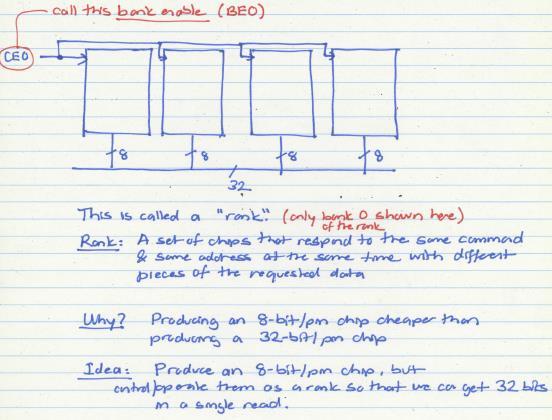
40 Rank 40
41 The DRAM Subsystem
42 DRAM Subsystem Organization Channel DIMM Rank Chip Bank Row/Column 42

43 The DRAM Bank Structure 43
44 Page Mode DRAM A DRAM bank is a 2D array of cells: rows x columns A DRAM row is also called a DRAM page Sense amplifiers also called row buffer Each address is a <row,column> pair Access to a closed row Activate command opens row (placed into row buffer) Read/write command reads/writes column in the row buffer Precharge command closes the row and prepares the bank for next access Access to an open row No need for activate command 44
45 Row decoder DRAM Bank Operation Access Address: (Row 0, Column 0) (Row 0, Column 1) (Row 0, Column 85) (Row 1, Column 0) Columns Row address 01 Rows Empty Row 01 Row Buffer CONFLICT HIT! Column address Column mux Data 45
46 The DRAM Chip Consists of multiple banks (2-16 in Synchronous DRAM) Banks share command/address/data buses The chip itself has a narrow interface (4-16 bits per read) 46
47 128M x 8-bit DRAM Chip 47
48 DRAM Rank and Module Rank: Multiple chips operated together to form a wide interface All chips comprising a rank are controlled at the same time Respond to a single command Share address and command buses, but provide different data A DRAM module consists of one or more ranks E.g., DIMM (dual inline memory module) This is what you plug into your motherboard If we have chips with 8-bit interface, to read 8 bytes in a single access, use 8 chips in a DIMM 48
49 A 64-bit Wide DIMM (One Rank) DRAM Chip DRAM Chip DRAM Chip DRAM Chip DRAM Chip DRAM Chip DRAM Chip DRAM Chip Command Data 49
50 A 64-bit Wide DIMM (One Rank) Advantages: Acts like a highcapacity DRAM chip with a wide interface Flexibility: memory controller does not need to deal with individual chips Disadvantages: Granularity: Accesses cannot be smaller than the interface width 50

51 Multiple DIMMs Advantages: Enables even higher capacity Disadvantages: Interconnect complexity and energy consumption can be high 51
52 DRAM Channels 2 Independent Channels: 2 Memory Controllers (Above) 2 Dependent/Lockstep Channels: 1 Memory Controller with wide interface (Not Shown above) 52
53 Generalized Memory Structure 53

54 Generalized Memory Structure 54
55 The DRAM Subsystem The Top Down View
56 DRAM Subsystem Organization Channel DIMM Rank Chip Bank Row/Column 56


57 The DRAM subsystem Channel DIMM (Dual in-line memory module) Processor Memory channel Memory channel
58 Breaking down a DIMM DIMM (Dual in-line memory module) Side view Front of DIMM Back of DIMM

59 Breaking down a DIMM DIMM (Dual in-line memory module) Side view Front of DIMM Back of DIMM Rank 0: collection of 8 chips Rank 1

60 Rank Rank 0 (Front) Rank 1 (Back) <0:63> <0:63> Addr/Cmd CS <0:1> Data <0:63> Memory channel
61 <0:7> <8:15> <56:63> Chip 0 Chip 1 Chip 7 Breaking down a Rank... Rank 0 <0:63> Data <0:63>


62 <0:7> <0:7> Chip 0 Breaking down a Chip Bank 0 <0:7> <0:7>... <0:7>

63 <0:7> <0:7> Breaking down a Bank 2kB 1B (column) row 16k-1 Bank 0... row 0 1B 1B Row-buffer... 1B
64 DRAM Subsystem Organization Channel DIMM Rank Chip Bank Row/Column 64


65 ... Example: Transferring a cache block Physical memory space 0xFFFF F Channel 0 DIMM 0 0x40 0x00 64B cache block Rank 0
66 <0:7> <8:15> <56:63>... Example: Transferring a cache block Physical memory space 0xFFFF F Chip 0 Chip 1 Chip 7 Rank x40 64B cache block Data <0:63> 0x00
67 <0:7> <8:15> <56:63>... Example: Transferring a cache block Physical memory space 0xFFFF F Row 0 Col 0 Chip 0 Chip 1 Chip 7 Rank x40 0x00 64B cache block Data <0:63>
68 <0:7> <8:15> <56:63>... Example: Transferring a cache block Physical memory space 0xFFFF F Row 0 Col 0 Chip 0 Chip 1 Chip 7 Rank x40 0x00 8B 64B cache block 8B Data <0:63>
69 <0:7> <8:15> <56:63>... Example: Transferring a cache block Physical memory space 0xFFFF F Row 0 Col 1 Chip 0 Chip 1 Chip 7 Rank x40 0x00 8B 64B cache block Data <0:63>
70 <0:7> <8:15> <56:63>... Example: Transferring a cache block Physical memory space 0xFFFF F Row 0 Col 1 Chip 0 Chip 1 Chip 7 Rank x40 0x00 8B 8B 64B cache block 8B Data <0:63>
71 <0:7> <8:15> <56:63>... Example: Transferring a cache block Physical memory space 0xFFFF F Row 0 Col 1 Chip 0 Chip 1 Chip 7 Rank x40 0x00 8B 8B 64B cache block Data <0:63> A 64B cache block takes 8 I/O cycles to transfer. During the process, 8 columns are read sequentially.
72 Latency Components: Basic DRAM Operation CPU controller transfer time Controller latency Queuing & scheduling delay at the controller Access converted to basic commands Controller DRAM transfer time DRAM bank latency Simple CAS if row is open OR RAS + CAS if array precharged OR PRE + RAS + CAS (worst case) DRAM CPU transfer time (through controller) 72
73 Multiple Banks (Interleaving) and Channels Multiple banks Enable concurrent DRAM accesses Bits in address determine which bank an address resides in Multiple independent channels serve the same purpose But they are even better because they have separate data buses Increased bus bandwidth Enabling more concurrency requires reducing Bank conflicts Channel conflicts How to select/randomize bank/channel indices in address? Lower order bits have more entropy Randomizing hash functions (XOR of different address bits) 73

74 How Multiple Banks/Channels Help 74
75 Multiple Channels Advantages Increased bandwidth Multiple concurrent accesses (if independent channels) Disadvantages Higher cost than a single channel More board wires More pins (if on-chip memory controller) 75
76 Address Mapping (Single Channel) Single-channel system with 8-byte memory bus 2GB memory, 8 banks, 16K rows & 2K columns per bank Row interleaving Consecutive rows of memory in consecutive banks Row (14 bits) Bank (3 bits) Column (11 bits) Byte in bus (3 bits) Cache block interleaving Consecutive cache block addresses in consecutive banks 64 byte cache blocks Row (14 bits) High Column Bank (3 bits) Low Col. Byte in bus (3 bits) 8 bits 3 bits Accesses to consecutive cache blocks can be serviced in parallel How about random accesses? Strided accesses? 76
77 Bank Mapping Randomization DRAM controller can randomize the address mapping to banks so that bank conflicts are less likely 3 bits Column (11 bits) Byte in bus (3 bits) XOR Bank index (3 bits) 77
78 Address Mapping (Multiple Channels) C Row (14 bits) Bank (3 bits) Column (11 bits) Byte in bus (3 bits) Row (14 bits) C Bank (3 bits) Column (11 bits) Byte in bus (3 bits) Row (14 bits) Bank (3 bits) C Column (11 bits) Byte in bus (3 bits) Row (14 bits) Bank (3 bits) Column (11 bits) C Byte in bus (3 bits) Where are consecutive cache blocks? C Row (14 bits) High Column Bank (3 bits) Low Col. Byte in bus (3 bits) 8 bits 3 bits Row (14 bits) C High Column Bank (3 bits) Low Col. Byte in bus (3 bits) 8 bits 3 bits Row (14 bits) High Column C Bank (3 bits) Low Col. Byte in bus (3 bits) 8 bits 3 bits Row (14 bits) High Column Bank (3 bits) C Low Col. Byte in bus (3 bits) 8 bits 3 bits Row (14 bits) High Column Bank (3 bits) Low Col. C Byte in bus (3 bits) 8 bits 3 bits 78
79 Interaction with VirtualPhysical Mapping Operating System influences where an address maps to in DRAM Virtual Page number (52 bits) Page offset (12 bits) VA Physical Frame number (19 bits) Page offset (12 bits) PA Row (14 bits) Bank (3 bits) Column (11 bits) Byte in bus (3 bits) PA Operating system can control which bank/channel/rank a virtual page is mapped to. It can perform page coloring to minimize bank conflicts Or to minimize inter-application interference 79
15-740/ Computer Architecture Lecture 19: Main Memory. Prof. Onur Mutlu Carnegie Mellon University
 15-740/18-740 Computer Architecture Lecture 19: Main Memory Prof. Onur Mutlu Carnegie Mellon University Last Time Multi-core issues in caching OS-based cache partitioning (using page coloring) Handling
EEM 486: Computer Architecture. Lecture 9. Memory
 EEM 486: Computer Architecture Lecture 9 Memory The Big Picture Designing a Multiple Clock Cycle Datapath Processor Control Memory Input Datapath Output The following slides belong to Prof. Onur Mutlu
Computer Architecture Lecture 21: Main Memory. Prof. Onur Mutlu Carnegie Mellon University Spring 2015, 3/23/2015
 18-447 Computer Architecture Lecture 21: Main Memory Prof. Onur Mutlu Carnegie Mellon University Spring 2015, 3/23/2015 Assignment Reminders Lab 6: Due April 3 C-level simulation of caches and branch prediction
Lecture-18 (Cache Optimizations) CS422-Spring
 CS422-Spring") Lecture-18 (Cache Optimizations) CS422-Spring 2018 Biswa@CSE-IITK Compiler Optimizations Loop interchange Merging Loop fusion Blocking Refer H&P: You need it for PA3 and PA4 too. CS422: Spring 2018 Biswabandan
Lecture-18 (Cache Optimizations) CS422-Spring 2018 Biswa@CSE-IITK Compiler Optimizations Loop interchange Merging Loop fusion Blocking Refer H&P: You need it for PA3 and PA4 too. CS422: Spring 2018 Biswabandan
15-740/ Computer Architecture Lecture 20: Main Memory II. Prof. Onur Mutlu Carnegie Mellon University
 15-740/18-740 Computer Architecture Lecture 20: Main Memory II Prof. Onur Mutlu Carnegie Mellon University Today SRAM vs. DRAM Interleaving/Banking DRAM Microarchitecture Memory controller Memory buses
18-447: Computer Architecture Lecture 17: Memory Hierarchy and Caches. Prof. Onur Mutlu Carnegie Mellon University Spring 2012, 3/26/2012
 18-447: Computer Architecture Lecture 17: Memory Hierarchy and Caches Prof. Onur Mutlu Carnegie Mellon University Spring 2012, 3/26/2012 Reminder: Homeworks Homework 5 Due April 2 Topics: Out-of-order
Advanced Caching Techniques (2) Department of Electrical Engineering Stanford University
 Department of Electrical Engineering Stanford University") Lecture 4: Advanced Caching Techniques (2) Department of Electrical Engineering Stanford University http://eeclass.stanford.edu/ee282 Lecture 4-1 Announcements HW1 is out (handout and online) Due on 10/15
Lecture 4: Advanced Caching Techniques (2) Department of Electrical Engineering Stanford University http://eeclass.stanford.edu/ee282 Lecture 4-1 Announcements HW1 is out (handout and online) Due on 10/15
15-740/ Computer Architecture Lecture 12: Advanced Caching. Prof. Onur Mutlu Carnegie Mellon University
 15-740/18-740 Computer Architecture Lecture 12: Advanced Caching Prof. Onur Mutlu Carnegie Mellon University Announcements Chuck Thacker (Microsoft Research) Seminar Tomorrow RARE: Rethinking Architectural
CS650 Computer Architecture. Lecture 9 Memory Hierarchy - Main Memory
 CS65 Computer Architecture Lecture 9 Memory Hierarchy - Main Memory Andrew Sohn Computer Science Department New Jersey Institute of Technology Lecture 9: Main Memory 9-/ /6/ A. Sohn Memory Cycle Time 5
CSE502: Computer Architecture CSE 502: Computer Architecture
 CSE 502: Computer Architecture Memory / DRAM SRAM = Static RAM SRAM vs. DRAM As long as power is present, data is retained DRAM = Dynamic RAM If you don t do anything, you lose the data SRAM: 6T per bit
Computer Architecture
 Computer Architecture Lecture 7: Memory Hierarchy and Caches Dr. Ahmed Sallam Suez Canal University Spring 2015 Based on original slides by Prof. Onur Mutlu Memory (Programmer s View) 2 Abstraction: Virtual
Lecture 15: DRAM Main Memory Systems. Today: DRAM basics and innovations (Section 2.3)
") Lecture 15: DRAM Main Memory Systems Today: DRAM basics and innovations (Section 2.3) 1 Memory Architecture Processor Memory Controller Address/Cmd Bank Row Buffer DIMM Data DIMM: a PCB with DRAM chips
Lecture 15: DRAM Main Memory Systems Today: DRAM basics and innovations (Section 2.3) 1 Memory Architecture Processor Memory Controller Address/Cmd Bank Row Buffer DIMM Data DIMM: a PCB with DRAM chips
18-447: Computer Architecture Lecture 22: Memory Hierarchy and Caches. Prof. Onur Mutlu Carnegie Mellon University Spring 2013, 3/27/2013
 18-447: Computer Architecture Lecture 22: Memory Hierarchy and Caches Prof. Onur Mutlu Carnegie Mellon University Spring 2013, 3/27/2013 Reminder: Homework 5 Due April 1 Topics: Vector processing, VLIW,
Computer Architecture Lecture 19: Memory Hierarchy and Caches. Prof. Onur Mutlu Carnegie Mellon University Spring 2013, 3/19/2014
 18-447 Computer Architecture Lecture 19: Memory Hierarchy and Caches Prof. Onur Mutlu Carnegie Mellon University Spring 2013, 3/19/2014 Extra Credit Recognition for Lab 3 1. John Greth (13157 ns) 2. Kevin
Lecture 14: Cache Innovations and DRAM. Today: cache access basics and innovations, DRAM (Sections )
") Lecture 14: Cache Innovations and DRAM Today: cache access basics and innovations, DRAM (Sections 5.1-5.3) 1 Reducing Miss Rate Large block size reduces compulsory misses, reduces miss penalty in case
Lecture 14: Cache Innovations and DRAM Today: cache access basics and innovations, DRAM (Sections 5.1-5.3) 1 Reducing Miss Rate Large block size reduces compulsory misses, reduces miss penalty in case
Computer Architecture Lecture 24: Memory Scheduling
 18-447 Computer Architecture Lecture 24: Memory Scheduling Prof. Onur Mutlu Presented by Justin Meza Carnegie Mellon University Spring 2014, 3/31/2014 Last Two Lectures Main Memory Organization and DRAM
Spring 2018 :: CSE 502. Main Memory & DRAM. Nima Honarmand
 Main Memory & DRAM Nima Honarmand Main Memory Big Picture 1) Last-level cache sends its memory requests to a Memory Controller Over a system bus of other types of interconnect 2) Memory controller translates
Lecture 17. Fall 2007 Prof. Thomas Wenisch. row enable. _bitline. Lecture 18 Slide 1 EECS 470
 Lecture 17 DRAM Memory row enable Fall 2007 Prof. Thomas Wenisch http://www.eecs.umich.edu/courses/eecs4 70 _bitline Slides developed in part by Profs. Austin, Brehob, Falsafi, Hill, Hoe, Lipasti, Shen,
Introduction to memory system :from device to system
 Introduction to memory system :from device to system Jianhui Yue Electrical and Computer Engineering University of Maine The Position of DRAM in the Computer 2 The Complexity of Memory 3 Question Assume
Chapter 5B. Large and Fast: Exploiting Memory Hierarchy
 Chapter 5B Large and Fast: Exploiting Memory Hierarchy One Transistor Dynamic RAM 1-T DRAM Cell word access transistor V REF TiN top electrode (V REF ) Ta 2 O 5 dielectric bit Storage capacitor (FET gate,
DRAM Main Memory. Dual Inline Memory Module (DIMM)
") DRAM Main Memory Dual Inline Memory Module (DIMM) Memory Technology Main memory serves as input and output to I/O interfaces and the processor. DRAMs for main memory, SRAM for caches Metrics: Latency,
DRAM Main Memory Dual Inline Memory Module (DIMM) Memory Technology Main memory serves as input and output to I/O interfaces and the processor. DRAMs for main memory, SRAM for caches Metrics: Latency,
Lecture: DRAM Main Memory. Topics: virtual memory wrap-up, DRAM intro and basics (Section 2.3)
") Lecture: DRAM Main Memory Topics: virtual memory wrap-up, DRAM intro and basics (Section 2.3) 1 TLB and Cache 2 Virtually Indexed Caches 24-bit virtual address, 4KB page size 12 bits offset and 12 bits
Lecture: DRAM Main Memory Topics: virtual memory wrap-up, DRAM intro and basics (Section 2.3) 1 TLB and Cache 2 Virtually Indexed Caches 24-bit virtual address, 4KB page size 12 bits offset and 12 bits
ELEC 5200/6200 Computer Architecture and Design Spring 2017 Lecture 7: Memory Organization Part II
 ELEC 5200/6200 Computer Architecture and Design Spring 2017 Lecture 7: Organization Part II Ujjwal Guin, Assistant Professor Department of Electrical and Computer Engineering Auburn University, Auburn,
Intro to Computer Architecture, Spring 2012 Midterm Exam II. Name:
 18-447 Intro to Computer Architecture, Spring 2012 Midterm Exam II Instructor: Onur Mutlu Teaching Assistants: Chris Fallin, Lavanya Subramanian, Abeer Agrawal Date: April 11, 2012 Name: Instructions:
Lecture: DRAM Main Memory. Topics: virtual memory wrap-up, DRAM intro and basics (Section 2.3)
") Lecture: DRAM Main Memory Topics: virtual memory wrap-up, DRAM intro and basics (Section 2.3) 1 TLB and Cache Is the cache indexed with virtual or physical address? To index with a physical address, we
Lecture: DRAM Main Memory Topics: virtual memory wrap-up, DRAM intro and basics (Section 2.3) 1 TLB and Cache Is the cache indexed with virtual or physical address? To index with a physical address, we
CS311 Lecture 21: SRAM/DRAM/FLASH
 S 14 L21-1 2014 CS311 Lecture 21: SRAM/DRAM/FLASH DARM part based on ISCA 2002 tutorial DRAM: Architectures, Interfaces, and Systems by Bruce Jacob and David Wang Jangwoo Kim (POSTECH) Thomas Wenisch (University
Intro to Computer Architecture, Spring 2012 Midterm Exam II
 18-447 Intro to Computer Architecture, Spring 2012 Midterm Exam II Instructor: Onur Mutlu Teaching Assistants: Chris Fallin, Lavanya Subramanian, Abeer Agrawal Date: April 11, 2012 Name: SOLUTIONS Problem
CSE502: Computer Architecture CSE 502: Computer Architecture
 CSE 502: Computer Architecture Memory / DRAM SRAM = Static RAM SRAM vs. DRAM As long as power is present, data is retained DRAM = Dynamic RAM If you don t do anything, you lose the data SRAM: 6T per bit
EE414 Embedded Systems Ch 5. Memory Part 2/2
 EE414 Embedded Systems Ch 5. Memory Part 2/2 Byung Kook Kim School of Electrical Engineering Korea Advanced Institute of Science and Technology Overview 6.1 introduction 6.2 Memory Write Ability and Storage
Multilevel Memories. Joel Emer Computer Science and Artificial Intelligence Laboratory Massachusetts Institute of Technology
 1 Multilevel Memories Computer Science and Artificial Intelligence Laboratory Massachusetts Institute of Technology Based on the material prepared by Krste Asanovic and Arvind CPU-Memory Bottleneck 6.823
Chapter 2: Memory Hierarchy Design (Part 3) Introduction Caches Main Memory (Section 2.2) Virtual Memory (Section 2.4, Appendix B.4, B.
 Introduction Caches Main Memory (Section 2.2) Virtual Memory (Section 2.4, Appendix B.4, B.") Chapter 2: Memory Hierarchy Design (Part 3) Introduction Caches Main Memory (Section 2.2) Virtual Memory (Section 2.4, Appendix B.4, B.5) Memory Technologies Dynamic Random Access Memory (DRAM) Optimized
Chapter 2: Memory Hierarchy Design (Part 3) Introduction Caches Main Memory (Section 2.2) Virtual Memory (Section 2.4, Appendix B.4, B.5) Memory Technologies Dynamic Random Access Memory (DRAM) Optimized
Portland State University ECE 587/687. Caches and Memory-Level Parallelism
 Portland State University ECE 587/687 Caches and Memory-Level Parallelism Revisiting Processor Performance Program Execution Time = (CPU clock cycles + Memory stall cycles) x clock cycle time For each
15-740/ Computer Architecture, Fall 2011 Midterm Exam II
 15-740/18-740 Computer Architecture, Fall 2011 Midterm Exam II Instructor: Onur Mutlu Teaching Assistants: Justin Meza, Yoongu Kim Date: December 2, 2011 Name: Instructions: Problem I (69 points) : Problem
Computer Architecture Spring 2016
 Computer Architecture Spring 2016 Lecture 08: Caches III Shuai Wang Department of Computer Science and Technology Nanjing University Improve Cache Performance Average memory access time (AMAT): AMAT =
15-740/ Computer Architecture Lecture 14: Runahead Execution. Prof. Onur Mutlu Carnegie Mellon University Fall 2011, 10/12/2011
 15-740/18-740 Computer Architecture Lecture 14: Runahead Execution Prof. Onur Mutlu Carnegie Mellon University Fall 2011, 10/12/2011 Reviews Due Today Chrysos and Emer, Memory Dependence Prediction Using
EN1640: Design of Computing Systems Topic 06: Memory System
 EN164: Design of Computing Systems Topic 6: Memory System Professor Sherief Reda http://scale.engin.brown.edu Electrical Sciences and Computer Engineering School of Engineering Brown University Spring
The DRAM Cell. EEC 581 Computer Architecture. Memory Hierarchy Design (III) 1T1C DRAM cell
 1T1C DRAM cell") EEC 581 Computer Architecture Memory Hierarchy Design (III) Department of Electrical Engineering and Computer Science Cleveland State University The DRAM Cell Word Line (Control) Bit Line (Information)
EEC 581 Computer Architecture Memory Hierarchy Design (III) Department of Electrical Engineering and Computer Science Cleveland State University The DRAM Cell Word Line (Control) Bit Line (Information)
Mark Redekopp, All rights reserved. EE 352 Unit 10. Memory System Overview SRAM vs. DRAM DMA & Endian-ness
 EE 352 Unit 10 Memory System Overview SRAM vs. DRAM DMA & Endian-ness The Memory Wall Problem: The Memory Wall Processor speeds have been increasing much faster than memory access speeds (Memory technology
Main Memory Systems. Department of Electrical Engineering Stanford University Lecture 5-1
 Lecture 5 Main Memory Systems Department of Electrical Engineering Stanford University http://eeclass.stanford.edu/ee282 Lecture 5-1 Announcements If you don t have a group of 3, contact us ASAP HW-1 is
Chapter 2: Memory Hierarchy Design Part 2
 Chapter 2: Memory Hierarchy Design Part 2 Introduction (Section 2.1, Appendix B) Caches Review of basics (Section 2.1, Appendix B) Advanced methods (Section 2.3) Main Memory Virtual Memory Fundamental
Reducing Hit Times. Critical Influence on cycle-time or CPI. small is always faster and can be put on chip
 Reducing Hit Times Critical Influence on cycle-time or CPI Keep L1 small and simple small is always faster and can be put on chip interesting compromise is to keep the tags on chip and the block data off
Memory. Lecture 22 CS301
 Memory Lecture 22 CS301 Administrative Daily Review of today s lecture w Due tomorrow (11/13) at 8am HW #8 due today at 5pm Program #2 due Friday, 11/16 at 11:59pm Test #2 Wednesday Pipelined Machine Fetch
CS250 VLSI Systems Design Lecture 9: Memory
 CS250 VLSI Systems esign Lecture 9: Memory John Wawrzynek, Jonathan Bachrach, with Krste Asanovic, John Lazzaro and Rimas Avizienis (TA) UC Berkeley Fall 2012 CMOS Bistable Flip State 1 0 0 1 Cross-coupled
Background. Memory Hierarchies. Register File. Background. Forecast Memory (B5) Motivation for memory hierarchy Cache ECC Virtual memory.
 Motivation for memory hierarchy Cache ECC Virtual memory.") Memory Hierarchies Forecast Memory (B5) Motivation for memory hierarchy Cache ECC Virtual memory Mem Element Background Size Speed Price Register small 1-5ns high?? SRAM medium 5-25ns $100-250 DRAM large
Memory Hierarchies Forecast Memory (B5) Motivation for memory hierarchy Cache ECC Virtual memory Mem Element Background Size Speed Price Register small 1-5ns high?? SRAM medium 5-25ns $100-250 DRAM large
The University of Adelaide, School of Computer Science 13 September 2018
 Computer Architecture A Quantitative Approach, Sixth Edition Chapter 2 Memory Hierarchy Design 1 Programmers want unlimited amounts of memory with low latency Fast memory technology is more expensive per
Reducing DRAM Latency at Low Cost by Exploiting Heterogeneity. Donghyuk Lee Carnegie Mellon University
 Reducing DRAM Latency at Low Cost by Exploiting Heterogeneity Donghyuk Lee Carnegie Mellon University Problem: High DRAM Latency processor stalls: waiting for data main memory high latency Major bottleneck
Mainstream Computer System Components
 Mainstream Computer System Components Double Date Rate (DDR) SDRAM One channel = 8 bytes = 64 bits wide Current DDR3 SDRAM Example: PC3-12800 (DDR3-1600) 200 MHz (internal base chip clock) 8-way interleaved
Intro to Computer Architecture, Spring 2012 Final Exam. Name:
 18-447 Intro to Computer Architecture, Spring 2012 Final Exam Instructor: Onur Mutlu Teaching Assistants: Chris Fallin, Lavanya Subramanian, Abeer Agrawal Date: May 10, 2012 Name: SOLUTIONS Problem I (190
CS698Y: Modern Memory Systems Lecture-16 (DRAM Timing Constraints) Biswabandan Panda
 Biswabandan Panda") CS698Y: Modern Memory Systems Lecture-16 (DRAM Timing Constraints) Biswabandan Panda biswap@cse.iitk.ac.in https://www.cse.iitk.ac.in/users/biswap/cs698y.html Row decoder Accessing a Row Access Address
CS698Y: Modern Memory Systems Lecture-16 (DRAM Timing Constraints) Biswabandan Panda biswap@cse.iitk.ac.in https://www.cse.iitk.ac.in/users/biswap/cs698y.html Row decoder Accessing a Row Access Address
Lecture-14 (Memory Hierarchy) CS422-Spring
 CS422-Spring") Lecture-14 (Memory Hierarchy) CS422-Spring 2018 Biswa@CSE-IITK The Ideal World Instruction Supply Pipeline (Instruction execution) Data Supply - Zero-cycle latency - Infinite capacity - Zero cost - Perfect
Lecture-14 (Memory Hierarchy) CS422-Spring 2018 Biswa@CSE-IITK The Ideal World Instruction Supply Pipeline (Instruction execution) Data Supply - Zero-cycle latency - Infinite capacity - Zero cost - Perfect
Lecture: Memory Technology Innovations
 Lecture: Memory Technology Innovations Topics: memory schedulers, refresh, state-of-the-art and upcoming changes: buffer chips, 3D stacking, non-volatile cells, photonics Multiprocessor intro 1 Row Buffers
CS152 Computer Architecture and Engineering Lecture 16: Memory System
 CS152 Computer Architecture and Engineering Lecture 16: System March 15, 1995 Dave Patterson (patterson@cs) and Shing Kong (shing.kong@eng.sun.com) Slides available on http://http.cs.berkeley.edu/~patterson
Embedded Systems Design: A Unified Hardware/Software Introduction. Outline. Chapter 5 Memory. Introduction. Memory: basic concepts
 Hardware/Software Introduction Chapter 5 Memory Outline Memory Write Ability and Storage Permanence Common Memory Types Composing Memory Memory Hierarchy and Cache Advanced RAM 1 2 Introduction Memory:
Embedded Systems Design: A Unified Hardware/Software Introduction. Chapter 5 Memory. Outline. Introduction
 Hardware/Software Introduction Chapter 5 Memory 1 Outline Memory Write Ability and Storage Permanence Common Memory Types Composing Memory Memory Hierarchy and Cache Advanced RAM 2 Introduction Embedded
Lecture 20: Memory Hierarchy Main Memory and Enhancing its Performance. Grinch-Like Stuff
 Lecture 20: ory Hierarchy Main ory and Enhancing its Performance Professor Alvin R. Lebeck Computer Science 220 Fall 1999 HW #4 Due November 12 Projects Finish reading Chapter 5 Grinch-Like Stuff CPS 220
Tiered-Latency DRAM: A Low Latency and A Low Cost DRAM Architecture
 Tiered-Latency DRAM: A Low Latency and A Low Cost DRAM Architecture Donghyuk Lee, Yoongu Kim, Vivek Seshadri, Jamie Liu, Lavanya Subramanian, Onur Mutlu Carnegie Mellon University HPCA - 2013 Executive
Computer Architecture: Main Memory (Part II) Prof. Onur Mutlu Carnegie Mellon University
 Prof. Onur Mutlu Carnegie Mellon University") Computer Architecture: Main Memory (Part II) Prof. Onur Mutlu Carnegie Mellon University Main Memory Lectures These slides are from the Scalable Memory Systems course taught at ACACES 2013 (July 15-19,
Computer Architecture: Main Memory (Part II) Prof. Onur Mutlu Carnegie Mellon University Main Memory Lectures These slides are from the Scalable Memory Systems course taught at ACACES 2013 (July 15-19,
Mainstream Computer System Components CPU Core 2 GHz GHz 4-way Superscaler (RISC or RISC-core (x86): Dynamic scheduling, Hardware speculation
: Dynamic scheduling, Hardware speculation") Mainstream Computer System Components CPU Core 2 GHz - 3.0 GHz 4-way Superscaler (RISC or RISC-core (x86): Dynamic scheduling, Hardware speculation One core or multi-core (2-4) per chip Multiple FP, integer
Mainstream Computer System Components CPU Core 2 GHz - 3.0 GHz 4-way Superscaler (RISC or RISC-core (x86): Dynamic scheduling, Hardware speculation One core or multi-core (2-4) per chip Multiple FP, integer
ECE 30 Introduction to Computer Engineering
 ECE 0 Introduction to Computer Engineering Study Problems, Set #9 Spring 01 1. Given the following series of address references given as word addresses:,,, 1, 1, 1,, 8, 19,,,,, 7,, and. Assuming a direct-mapped
An introduction to SDRAM and memory controllers. 5kk73
 An introduction to SDRAM and memory controllers 5kk73 Presentation Outline (part 1) Introduction to SDRAM Basic SDRAM operation Memory efficiency SDRAM controller architecture Conclusions Followed by part
CS252 S05. Main memory management. Memory hardware. The scale of things. Memory hardware (cont.) Bottleneck
 Bottleneck") Main memory management CMSC 411 Computer Systems Architecture Lecture 16 Memory Hierarchy 3 (Main Memory & Memory) Questions: How big should main memory be? How to handle reads and writes? How to find
Main memory management CMSC 411 Computer Systems Architecture Lecture 16 Memory Hierarchy 3 (Main Memory & Memory) Questions: How big should main memory be? How to handle reads and writes? How to find
15-740/ Computer Architecture Lecture 21: Superscalar Processing. Prof. Onur Mutlu Carnegie Mellon University
 15-740/18-740 Computer Architecture Lecture 21: Superscalar Processing Prof. Onur Mutlu Carnegie Mellon University Announcements Project Milestone 2 Due November 10 Homework 4 Out today Due November 15
CSE 431 Computer Architecture Fall Chapter 5A: Exploiting the Memory Hierarchy, Part 1
 CSE 431 Computer Architecture Fall 2008 Chapter 5A: Exploiting the Memory Hierarchy, Part 1 Mary Jane Irwin ( www.cse.psu.edu/~mji ) [Adapted from Computer Organization and Design, 4 th Edition, Patterson
ECE 485/585 Microprocessor System Design
 Microprocessor System Design Lecture 5: Zeshan Chishti DRAM Basics DRAM Evolution SDRAM-based Memory Systems Electrical and Computer Engineering Dept. Maseeh College of Engineering and Computer Science
Memory System Overview. DMA & Endian-ness. Technology. Architectural. Problem: The Memory Wall
 The Memory Wall EE 357 Unit 13 Problem: The Memory Wall Processor speeds have been increasing much faster than memory access speeds (Memory technology targets density rather than speed) Large memories
Chapter 2: Memory Hierarchy Design Part 2
 Chapter 2: Memory Hierarchy Design Part 2 Introduction (Section 2.1, Appendix B) Caches Review of basics (Section 2.1, Appendix B) Advanced methods (Section 2.3) Main Memory Virtual Memory Fundamental
Why memory hierarchy? Memory hierarchy. Memory hierarchy goals. CS2410: Computer Architecture. L1 cache design. Sangyeun Cho
 Why memory hierarchy? L1 cache design Sangyeun Cho Computer Science Department Memory hierarchy Memory hierarchy goals Smaller Faster More expensive per byte CPU Regs L1 cache L2 cache SRAM SRAM To provide
Memory latency: Affects cache miss penalty. Measured by:
 Main Memory Main memory generally utilizes Dynamic RAM (DRAM), which use a single transistor to store a bit, but require a periodic data refresh by reading every row. Static RAM may be used for main memory
CS 152 Computer Architecture and Engineering. Lecture 7 - Memory Hierarchy-II
 CS 152 Computer Architecture and Engineering Lecture 7 - Memory Hierarchy-II Krste Asanovic Electrical Engineering and Computer Sciences University of California at Berkeley http://www.eecs.berkeley.edu/~krste
15-740/ Computer Architecture
 15-740/18-740 Computer Architecture Lecture 19: Caching II Prof. Onur Mutlu Carnegie Mellon University Fall 2011, 10/31/2011 Announcements Milestone II Due November 4, Friday Please talk with us if you
Computer Systems Architecture I. CSE 560M Lecture 18 Guest Lecturer: Shakir James
 Computer Systems Architecture I CSE 560M Lecture 18 Guest Lecturer: Shakir James Plan for Today Announcements No class meeting on Monday, meet in project groups Project demos < 2 weeks, Nov 23 rd Questions
Lecture 18: Memory Hierarchy Main Memory and Enhancing its Performance Professor Randy H. Katz Computer Science 252 Spring 1996
 Lecture 18: Memory Hierarchy Main Memory and Enhancing its Performance Professor Randy H. Katz Computer Science 252 Spring 1996 RHK.S96 1 Review: Reducing Miss Penalty Summary Five techniques Read priority
Lecture: Memory, Multiprocessors. Topics: wrap-up of memory systems, intro to multiprocessors and multi-threaded programming models
 Lecture: Memory, Multiprocessors Topics: wrap-up of memory systems, intro to multiprocessors and multi-threaded programming models 1 Refresh Every DRAM cell must be refreshed within a 64 ms window A row
Portland State University ECE 587/687. Caches and Memory-Level Parallelism
 Portland State University ECE 587/687 Caches and Memory-Level Parallelism Copyright by Alaa Alameldeen, Zeshan Chishti and Haitham Akkary 2017 Revisiting Processor Performance Program Execution Time =
TDT Coarse-Grained Multithreading. Review on ILP. Multi-threaded execution. Contents. Fine-Grained Multithreading
 Review on ILP TDT 4260 Chap 5 TLP & Hierarchy What is ILP? Let the compiler find the ILP Advantages? Disadvantages? Let the HW find the ILP Advantages? Disadvantages? Contents Multi-threading Chap 3.5
EN1640: Design of Computing Systems Topic 06: Memory System
 EN164: Design of Computing Systems Topic 6: Memory System Professor Sherief Reda http://scale.engin.brown.edu Electrical Sciences and Computer Engineering School of Engineering Brown University Spring
Lecture notes for CS Chapter 2, part 1 10/23/18
 Chapter 2: Memory Hierarchy Design Part 2 Introduction (Section 2.1, Appendix B) Caches Review of basics (Section 2.1, Appendix B) Advanced methods (Section 2.3) Main Memory Virtual Memory Fundamental
The Memory Hierarchy & Cache
 Removing The Ideal Memory Assumption: The Memory Hierarchy & Cache The impact of real memory on CPU Performance. Main memory basic properties: Memory Types: DRAM vs. SRAM The Motivation for The Memory
EC 513 Computer Architecture
 EC 513 Computer Architecture Cache Organization Prof. Michel A. Kinsy The course has 4 modules Module 1 Instruction Set Architecture (ISA) Simple Pipelining and Hazards Module 2 Superscalar Architectures
CPE300: Digital System Architecture and Design
 CPE300: Digital System Architecture and Design Fall 2011 MW 17:30-18:45 CBC C316 Cache 11232011 http://www.egr.unlv.edu/~b1morris/cpe300/ 2 Outline Review Memory Components/Boards Two-Level Memory Hierarchy
15-740/ Computer Architecture Lecture 23: Superscalar Processing (III) Prof. Onur Mutlu Carnegie Mellon University
 Prof. Onur Mutlu Carnegie Mellon University") 15-740/18-740 Computer Architecture Lecture 23: Superscalar Processing (III) Prof. Onur Mutlu Carnegie Mellon University Announcements Homework 4 Out today Due November 15 Midterm II November 22 Project
15-740/18-740 Computer Architecture Lecture 23: Superscalar Processing (III) Prof. Onur Mutlu Carnegie Mellon University Announcements Homework 4 Out today Due November 15 Midterm II November 22 Project
LECTURE 5: MEMORY HIERARCHY DESIGN
 LECTURE 5: MEMORY HIERARCHY DESIGN Abridged version of Hennessy & Patterson (2012):Ch.2 Introduction Programmers want unlimited amounts of memory with low latency Fast memory technology is more expensive
Internal Memory. Computer Architecture. Outline. Memory Hierarchy. Semiconductor Memory Types. Copyright 2000 N. AYDIN. All rights reserved.
 Computer Architecture Prof. Dr. Nizamettin AYDIN naydin@yildiz.edu.tr nizamettinaydin@gmail.com Internal Memory http://www.yildiz.edu.tr/~naydin 1 2 Outline Semiconductor main memory Random Access Memory
Memory latency: Affects cache miss penalty. Measured by:
 Main Memory Main memory generally utilizes Dynamic RAM (DRAM), which use a single transistor to store a bit, but require a periodic data refresh by reading every row. Static RAM may be used for main memory
ECE 485/585 Microprocessor System Design
 Microprocessor System Design Lecture 7: Memory Modules Error Correcting Codes Memory Controllers Zeshan Chishti Electrical and Computer Engineering Dept. Maseeh College of Engineering and Computer Science
CpE 442. Memory System
 CpE 442 Memory System CPE 442 memory.1 Outline of Today s Lecture Recap and Introduction (5 minutes) Memory System: the BIG Picture? (15 minutes) Memory Technology: SRAM and Register File (25 minutes)
15-740/ Computer Architecture
 15-740/18-740 Computer Architecture Lecture 16: Runahead and OoO Wrap-Up Prof. Onur Mutlu Carnegie Mellon University Fall 2011, 10/17/2011 Review Set 9 Due this Wednesday (October 19) Wilkes, Slave Memories
Copyright 2012, Elsevier Inc. All rights reserved.
 Computer Architecture A Quantitative Approach, Fifth Edition Chapter 2 Memory Hierarchy Design 1 Introduction Introduction Programmers want unlimited amounts of memory with low latency Fast memory technology
Computer Architecture. A Quantitative Approach, Fifth Edition. Chapter 2. Memory Hierarchy Design. Copyright 2012, Elsevier Inc. All rights reserved.
 Computer Architecture A Quantitative Approach, Fifth Edition Chapter 2 Memory Hierarchy Design 1 Programmers want unlimited amounts of memory with low latency Fast memory technology is more expensive per
Basics DRAM ORGANIZATION. Storage element (capacitor) Data In/Out Buffers. Word Line. Bit Line. Switching element HIGH-SPEED MEMORY SYSTEMS
 Data In/Out Buffers. Word Line. Bit Line. Switching element HIGH-SPEED MEMORY SYSTEMS") Basics DRAM ORGANIZATION DRAM Word Line Bit Line Storage element (capacitor) In/Out Buffers Decoder Sense Amps... Bit Lines... Switching element Decoder... Word Lines... Memory Array Page 1 Basics BUS
Basics DRAM ORGANIZATION DRAM Word Line Bit Line Storage element (capacitor) In/Out Buffers Decoder Sense Amps... Bit Lines... Switching element Decoder... Word Lines... Memory Array Page 1 Basics BUS
Memories: Memory Technology
 Memories: Memory Technology Z. Jerry Shi Assistant Professor of Computer Science and Engineering University of Connecticut * Slides adapted from Blumrich&Gschwind/ELE475 03, Peh/ELE475 * Memory Hierarchy
CS 33. Architecture and Optimization (3) CS33 Intro to Computer Systems XVI 1 Copyright 2018 Thomas W. Doeppner. All rights reserved.
 CS33 Intro to Computer Systems XVI 1 Copyright 2018 Thomas W. Doeppner. All rights reserved.") CS 33 Architecture and Optimization (3) CS33 Intro to Computer Systems XVI 1 Copyright 2018 Thomas W. Doeppner. All rights reserved. Hyper Threading Instruction Control Instruction Control Retirement Unit
CS 33 Architecture and Optimization (3) CS33 Intro to Computer Systems XVI 1 Copyright 2018 Thomas W. Doeppner. All rights reserved. Hyper Threading Instruction Control Instruction Control Retirement Unit
Main Memory. EECC551 - Shaaban. Memory latency: Affects cache miss penalty. Measured by:
 Main Memory Main memory generally utilizes Dynamic RAM (DRAM), which use a single transistor to store a bit, but require a periodic data refresh by reading every row (~every 8 msec). Static RAM may be
COSC 6385 Computer Architecture - Memory Hierarchies (II)
") COSC 6385 Computer Architecture - Memory Hierarchies (II) Edgar Gabriel Spring 2018 Types of cache misses Compulsory Misses: first access to a block cannot be in the cache (cold start misses) Capacity
COSC 6385 Computer Architecture - Memory Hierarchies (II) Edgar Gabriel Spring 2018 Types of cache misses Compulsory Misses: first access to a block cannot be in the cache (cold start misses) Capacity
The Memory Hierarchy 1
 The Memory Hierarchy 1 What is a cache? 2 What problem do caches solve? 3 Memory CPU Abstraction: Big array of bytes Memory memory 4 Performance vs 1980 Processor vs Memory Performance Memory is very slow
Evaluating STT-RAM as an Energy-Efficient Main Memory Alternative
 Evaluating STT-RAM as an Energy-Efficient Main Memory Alternative Emre Kültürsay *, Mahmut Kandemir *, Anand Sivasubramaniam *, and Onur Mutlu * Pennsylvania State University Carnegie Mellon University
Copyright 2012, Elsevier Inc. All rights reserved.
 Computer Architecture A Quantitative Approach, Fifth Edition Chapter 2 Memory Hierarchy Design 1 Introduction Programmers want unlimited amounts of memory with low latency Fast memory technology is more
Donn Morrison Department of Computer Science. TDT4255 Memory hierarchies
 TDT4255 Lecture 10: Memory hierarchies Donn Morrison Department of Computer Science 2 Outline Chapter 5 - Memory hierarchies (5.1-5.5) Temporal and spacial locality Hits and misses Direct-mapped, set associative,
Views of Memory. Real machines have limited amounts of memory. Programmer doesn t want to be bothered. 640KB? A few GB? (This laptop = 2GB)
") CS6290 Memory Views of Memory Real machines have limited amounts of memory 640KB? A few GB? (This laptop = 2GB) Programmer doesn t want to be bothered Do you think, oh, this computer only has 128MB so
CS6290 Memory Views of Memory Real machines have limited amounts of memory 640KB? A few GB? (This laptop = 2GB) Programmer doesn t want to be bothered Do you think, oh, this computer only has 128MB so
Chapter 5A. Large and Fast: Exploiting Memory Hierarchy
 Chapter 5A Large and Fast: Exploiting Memory Hierarchy Memory Technology Static RAM (SRAM) Fast, expensive Dynamic RAM (DRAM) In between Magnetic disk Slow, inexpensive Ideal memory Access time of SRAM