DRAM Main Memory. Dual Inline Memory Module (DIMM)
|
|
|
- Camilla Stone
- 5 years ago
- Views:
Transcription

1 DRAM Main Memory Dual Inline Memory Module (DIMM)
2 Memory Technology Main memory serves as input and output to I/O interfaces and the processor. DRAMs for main memory, SRAM for caches Metrics: Latency, Bandwidth Access Time Time between read request and when desired word arrives Cycle Time Minimum time between unrelated requests to memory
3 DRAM SRAM Requires low power to retain bit, 6 transistors/bit Dynamic Random Access Memory (DRAM) 8x more dense than SRAM Dynamic: Charge leak, Must be re-written after being read Must be periodically refreshed Every ~ 8 ms
4 DRAM
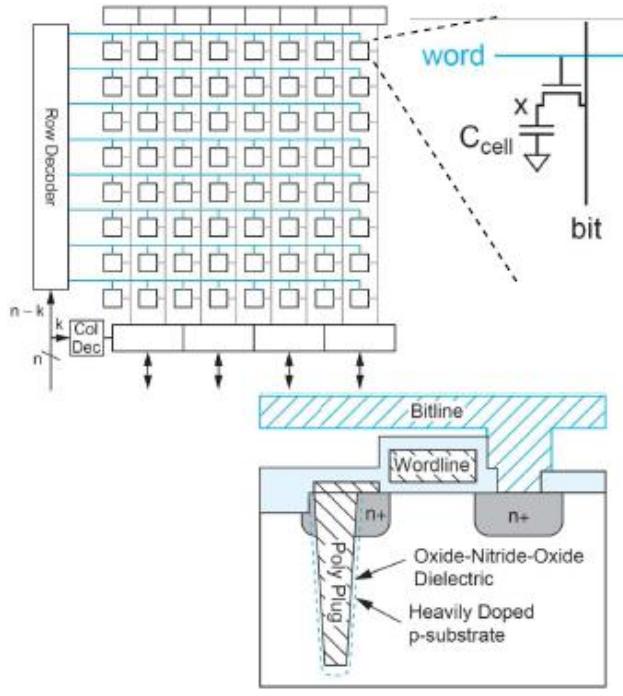
5 DRAM Array Row Decoder Row Address Strobe (RAS) 12b Memory Cell Array Array Size 4096b x 4096b 16 Mb Sense Amps Row Buffer RAS and CAS are delivered in consecutive cycles Column Address Strobe (CAS) 12b Column Decoder Data Bus 34b address identifies the 64B unit to fetch from DRAM DRAM can address 40b data (1 Tb)
 + 1GB (Rank 2) = 2GB per module. http://www.anandtech.com/")
6 DRAM Hierarchy 128MB = 16,384 rows/bank x 1,024 columns addresses/row x 1 byte/column address x 8 stacked banks per IC. 128MB x 8 ICs per rank = 1GB in Rank 1. 1GB (Rank 1) + 1GB (Rank 2) = 2GB per module.
7 Main Memory Memory Channel = Data (64b) + Address/Cmd (23b = 17a + 6c) DIMM: a PCB with DRAM chips on the back and front Transfers one cache line size (64B) per address
8 Main Memory 17a + 6c 64b = (4 x16 or 8 x8 or 16 x4 or...) DIMM RANK 8b 64b on Bus
9 Main Memory Row buffer: the last row (say, 8 KB) read from a bank, acts like a cache Bank: a subset of a rank that is busy during one request 4, 8 or 16 in one chip Rank: a collection of DRAM chips that work together to respond to a request and keep the data bus full TWO BANKS ROW BUFFER
10 Row Buffers Each bank has a single row buffer Row buffers act as a cache within DRAM Row buffer hit: ~20 ns access time (time to move data from row buffer to pins) Empty row buffer access: ~40 ns (read arrays + move data from row buffer to pins) Row buffer conflict: ~60 ns (precharge bitlines + read new row + move data to pins) Waiting time in the Queue (tens of nano-seconds) and incur address/cmd/data transfer delays (~10 ns)
11 Open/Closed Page Policies Open Page Policy: Row buffers are kept open Useful when access stream has locality Row buffer hits are cheap (20ns) Row buffer miss is a bank conflict and expensive (60ns) Closed Page Policy: Bitlines are precharged immediately after access Useful when access stream has little locality Nearly every access is a row buffer miss (40ns) The precharge is usually not on the critical path Modern memory controller policies lie somewhere between these two extremes (usually proprietary)
12 Reads and Writes A single bus is used for reads and writes Bus direction must be reversed when switching between reads and writes Takes time and leads to bus idling Writes are performed in bursts Write queue stores pending writes until a high watermark is reached
13 Memory Controller Read Queue Scheduler Scheduler FCFS, First Ready-FCFS, Stall Time Fair Response Queue Write Queue Buffer Buffer
14 Address Mapping Policies Consecutive cache lines can be placed in the same row to boost row buffer hit rates row:rank:bank:channel:column:blkoffset Time between access to cache block and +1 = 20ns (row buffer hit)
15 Address Mapping Policies Consecutive cache lines can be placed in different ranks to boost parallelism row:column:rank:bank:channel:blkoffset MC MC1 Multicore MulticoreProcessor Processor Cache blocks and +1 can be accessed simultaneously
16 DRAM Refresh Every DRAM cell must be refreshed within a 64 ms window A row read/write automatically refreshes the row Every refresh command performs refresh on a number of rows, the memory system is unavailable during that time A refresh command is issued by the memory controller once every 7.8μs on average 8192 rows in RAM. 64ms/8192 = 7.8μs
17 Error Correction SECDED single error correct double error detect 8b code for every 64-bit word A rank is now made up of 9 x8 chips, instead of 8 x8 chips Stronger forms of error protection exist: a system is chipkill correct if it can handle an entire DRAM chip failure

18 Modern Memory System
 Boosts processor pin bandwidth and memory capacity More expensive, high")
19 Modern Memory System The link into the processor is narrow and high frequency The Scalable Memory Buffer chip is a router that connects to multiple DDR3 channels (wide and slow) Boosts processor pin bandwidth and memory capacity More expensive, high power
20 Future Memory Trends Processor pin count is not increasing High memory bandwidth requires high pin frequency 3D stacking can enable high memory capacity and high channel frequency (e.g., Micron HMC) Phase Change Memory cells Silicon Photonics
21 References Rajeev Balasubramonian, CS6810 Computer Architecture. University of Utah. Hennessy and Patterson. Computer Architecture. 5e. MK. Appendix B, Chapter 2. Bruce Jacob, Spencer Ng, David Wang. Memory Systems: Cache, DRAM. Elsevier, 2007.
Lecture 15: DRAM Main Memory Systems. Today: DRAM basics and innovations (Section 2.3)
") Lecture 15: DRAM Main Memory Systems Today: DRAM basics and innovations (Section 2.3) 1 Memory Architecture Processor Memory Controller Address/Cmd Bank Row Buffer DIMM Data DIMM: a PCB with DRAM chips
Lecture 15: DRAM Main Memory Systems Today: DRAM basics and innovations (Section 2.3) 1 Memory Architecture Processor Memory Controller Address/Cmd Bank Row Buffer DIMM Data DIMM: a PCB with DRAM chips
M2 Outline. Memory Hierarchy Cache Blocking Cache Aware Programming SRAM, DRAM Virtual Memory Virtual Machines Non-volatile Memory, Persistent NVM
 M2 Memory Systems M2 Outline Memory Hierarchy Cache Blocking Cache Aware Programming SRAM, DRAM Virtual Memory Virtual Machines Non-volatile Memory, Persistent NVM Memory Technology Memory MemoryArrays
Lecture: Memory Technology Innovations
 Lecture: Memory Technology Innovations Topics: memory schedulers, refresh, state-of-the-art and upcoming changes: buffer chips, 3D stacking, non-volatile cells, photonics Multiprocessor intro 1 Row Buffers
Lecture: DRAM Main Memory. Topics: virtual memory wrap-up, DRAM intro and basics (Section 2.3)
") Lecture: DRAM Main Memory Topics: virtual memory wrap-up, DRAM intro and basics (Section 2.3) 1 TLB and Cache Is the cache indexed with virtual or physical address? To index with a physical address, we
Lecture: DRAM Main Memory Topics: virtual memory wrap-up, DRAM intro and basics (Section 2.3) 1 TLB and Cache Is the cache indexed with virtual or physical address? To index with a physical address, we
Lecture: DRAM Main Memory. Topics: virtual memory wrap-up, DRAM intro and basics (Section 2.3)
") Lecture: DRAM Main Memory Topics: virtual memory wrap-up, DRAM intro and basics (Section 2.3) 1 TLB and Cache 2 Virtually Indexed Caches 24-bit virtual address, 4KB page size 12 bits offset and 12 bits
Lecture: DRAM Main Memory Topics: virtual memory wrap-up, DRAM intro and basics (Section 2.3) 1 TLB and Cache 2 Virtually Indexed Caches 24-bit virtual address, 4KB page size 12 bits offset and 12 bits
Lecture: Memory, Multiprocessors. Topics: wrap-up of memory systems, intro to multiprocessors and multi-threaded programming models
 Lecture: Memory, Multiprocessors Topics: wrap-up of memory systems, intro to multiprocessors and multi-threaded programming models 1 Refresh Every DRAM cell must be refreshed within a 64 ms window A row
Lecture: Memory, Coherence Protocols. Topics: wrap-up of memory systems, intro to multi-thread programming models
 Lecture: Memory, Coherence Protocols Topics: wrap-up of memory systems, intro to multi-thread programming models 1 Refresh Every DRAM cell must be refreshed within a 64 ms window A row read/write automatically
CS698Y: Modern Memory Systems Lecture-16 (DRAM Timing Constraints) Biswabandan Panda
 Biswabandan Panda") CS698Y: Modern Memory Systems Lecture-16 (DRAM Timing Constraints) Biswabandan Panda biswap@cse.iitk.ac.in https://www.cse.iitk.ac.in/users/biswap/cs698y.html Row decoder Accessing a Row Access Address
CS698Y: Modern Memory Systems Lecture-16 (DRAM Timing Constraints) Biswabandan Panda biswap@cse.iitk.ac.in https://www.cse.iitk.ac.in/users/biswap/cs698y.html Row decoder Accessing a Row Access Address
EEM 486: Computer Architecture. Lecture 9. Memory
 EEM 486: Computer Architecture Lecture 9 Memory The Big Picture Designing a Multiple Clock Cycle Datapath Processor Control Memory Input Datapath Output The following slides belong to Prof. Onur Mutlu
15-740/ Computer Architecture Lecture 19: Main Memory. Prof. Onur Mutlu Carnegie Mellon University
 15-740/18-740 Computer Architecture Lecture 19: Main Memory Prof. Onur Mutlu Carnegie Mellon University Last Time Multi-core issues in caching OS-based cache partitioning (using page coloring) Handling
The University of Adelaide, School of Computer Science 13 September 2018
 Computer Architecture A Quantitative Approach, Sixth Edition Chapter 2 Memory Hierarchy Design 1 Programmers want unlimited amounts of memory with low latency Fast memory technology is more expensive per
COSC 6385 Computer Architecture - Memory Hierarchies (III)
") COSC 6385 Computer Architecture - Memory Hierarchies (III) Edgar Gabriel Spring 2014 Memory Technology Performance metrics Latency problems handled through caches Bandwidth main concern for main memory
COSC 6385 Computer Architecture - Memory Hierarchies (III) Edgar Gabriel Spring 2014 Memory Technology Performance metrics Latency problems handled through caches Bandwidth main concern for main memory
Chapter 2: Memory Hierarchy Design (Part 3) Introduction Caches Main Memory (Section 2.2) Virtual Memory (Section 2.4, Appendix B.4, B.
 Introduction Caches Main Memory (Section 2.2) Virtual Memory (Section 2.4, Appendix B.4, B.") Chapter 2: Memory Hierarchy Design (Part 3) Introduction Caches Main Memory (Section 2.2) Virtual Memory (Section 2.4, Appendix B.4, B.5) Memory Technologies Dynamic Random Access Memory (DRAM) Optimized
Chapter 2: Memory Hierarchy Design (Part 3) Introduction Caches Main Memory (Section 2.2) Virtual Memory (Section 2.4, Appendix B.4, B.5) Memory Technologies Dynamic Random Access Memory (DRAM) Optimized
CS311 Lecture 21: SRAM/DRAM/FLASH
 S 14 L21-1 2014 CS311 Lecture 21: SRAM/DRAM/FLASH DARM part based on ISCA 2002 tutorial DRAM: Architectures, Interfaces, and Systems by Bruce Jacob and David Wang Jangwoo Kim (POSTECH) Thomas Wenisch (University
The DRAM Cell. EEC 581 Computer Architecture. Memory Hierarchy Design (III) 1T1C DRAM cell
 1T1C DRAM cell") EEC 581 Computer Architecture Memory Hierarchy Design (III) Department of Electrical Engineering and Computer Science Cleveland State University The DRAM Cell Word Line (Control) Bit Line (Information)
EEC 581 Computer Architecture Memory Hierarchy Design (III) Department of Electrical Engineering and Computer Science Cleveland State University The DRAM Cell Word Line (Control) Bit Line (Information)
COSC 6385 Computer Architecture - Memory Hierarchies (II)
") COSC 6385 Computer Architecture - Memory Hierarchies (II) Edgar Gabriel Spring 2018 Types of cache misses Compulsory Misses: first access to a block cannot be in the cache (cold start misses) Capacity
COSC 6385 Computer Architecture - Memory Hierarchies (II) Edgar Gabriel Spring 2018 Types of cache misses Compulsory Misses: first access to a block cannot be in the cache (cold start misses) Capacity
LECTURE 5: MEMORY HIERARCHY DESIGN
 LECTURE 5: MEMORY HIERARCHY DESIGN Abridged version of Hennessy & Patterson (2012):Ch.2 Introduction Programmers want unlimited amounts of memory with low latency Fast memory technology is more expensive
Spring 2018 :: CSE 502. Main Memory & DRAM. Nima Honarmand
 Main Memory & DRAM Nima Honarmand Main Memory Big Picture 1) Last-level cache sends its memory requests to a Memory Controller Over a system bus of other types of interconnect 2) Memory controller translates
18-447: Computer Architecture Lecture 25: Main Memory. Prof. Onur Mutlu Carnegie Mellon University Spring 2013, 4/3/2013
 18-447: Computer Architecture Lecture 25: Main Memory Prof. Onur Mutlu Carnegie Mellon University Spring 2013, 4/3/2013 Reminder: Homework 5 (Today) Due April 3 (Wednesday!) Topics: Vector processing,
Introduction to memory system :from device to system
 Introduction to memory system :from device to system Jianhui Yue Electrical and Computer Engineering University of Maine The Position of DRAM in the Computer 2 The Complexity of Memory 3 Question Assume
Chapter 5B. Large and Fast: Exploiting Memory Hierarchy
 Chapter 5B Large and Fast: Exploiting Memory Hierarchy One Transistor Dynamic RAM 1-T DRAM Cell word access transistor V REF TiN top electrode (V REF ) Ta 2 O 5 dielectric bit Storage capacitor (FET gate,
Computer Architecture A Quantitative Approach, Fifth Edition. Chapter 2. Memory Hierarchy Design. Copyright 2012, Elsevier Inc. All rights reserved.
 Computer Architecture A Quantitative Approach, Fifth Edition Chapter 2 Memory Hierarchy Design 1 Introduction Programmers want unlimited amounts of memory with low latency Fast memory technology is more
ECE 485/585 Microprocessor System Design
 Microprocessor System Design Lecture 5: Zeshan Chishti DRAM Basics DRAM Evolution SDRAM-based Memory Systems Electrical and Computer Engineering Dept. Maseeh College of Engineering and Computer Science
Adapted from David Patterson s slides on graduate computer architecture
 Mei Yang Adapted from David Patterson s slides on graduate computer architecture Introduction Ten Advanced Optimizations of Cache Performance Memory Technology and Optimizations Virtual Memory and Virtual
Multilevel Memories. Joel Emer Computer Science and Artificial Intelligence Laboratory Massachusetts Institute of Technology
 1 Multilevel Memories Computer Science and Artificial Intelligence Laboratory Massachusetts Institute of Technology Based on the material prepared by Krste Asanovic and Arvind CPU-Memory Bottleneck 6.823
Mark Redekopp, All rights reserved. EE 352 Unit 10. Memory System Overview SRAM vs. DRAM DMA & Endian-ness
 EE 352 Unit 10 Memory System Overview SRAM vs. DRAM DMA & Endian-ness The Memory Wall Problem: The Memory Wall Processor speeds have been increasing much faster than memory access speeds (Memory technology
Basics DRAM ORGANIZATION. Storage element (capacitor) Data In/Out Buffers. Word Line. Bit Line. Switching element HIGH-SPEED MEMORY SYSTEMS
 Data In/Out Buffers. Word Line. Bit Line. Switching element HIGH-SPEED MEMORY SYSTEMS") Basics DRAM ORGANIZATION DRAM Word Line Bit Line Storage element (capacitor) In/Out Buffers Decoder Sense Amps... Bit Lines... Switching element Decoder... Word Lines... Memory Array Page 1 Basics BUS
Basics DRAM ORGANIZATION DRAM Word Line Bit Line Storage element (capacitor) In/Out Buffers Decoder Sense Amps... Bit Lines... Switching element Decoder... Word Lines... Memory Array Page 1 Basics BUS
CSE502: Computer Architecture CSE 502: Computer Architecture
 CSE 502: Computer Architecture Memory / DRAM SRAM = Static RAM SRAM vs. DRAM As long as power is present, data is retained DRAM = Dynamic RAM If you don t do anything, you lose the data SRAM: 6T per bit
Copyright 2012, Elsevier Inc. All rights reserved.
 Computer Architecture A Quantitative Approach, Fifth Edition Chapter 2 Memory Hierarchy Design 1 Introduction Introduction Programmers want unlimited amounts of memory with low latency Fast memory technology
Computer Architecture. A Quantitative Approach, Fifth Edition. Chapter 2. Memory Hierarchy Design. Copyright 2012, Elsevier Inc. All rights reserved.
 Computer Architecture A Quantitative Approach, Fifth Edition Chapter 2 Memory Hierarchy Design 1 Programmers want unlimited amounts of memory with low latency Fast memory technology is more expensive per
Lecture 14: Cache Innovations and DRAM. Today: cache access basics and innovations, DRAM (Sections )
") Lecture 14: Cache Innovations and DRAM Today: cache access basics and innovations, DRAM (Sections 5.1-5.3) 1 Reducing Miss Rate Large block size reduces compulsory misses, reduces miss penalty in case
Lecture 14: Cache Innovations and DRAM Today: cache access basics and innovations, DRAM (Sections 5.1-5.3) 1 Reducing Miss Rate Large block size reduces compulsory misses, reduces miss penalty in case
Copyright 2012, Elsevier Inc. All rights reserved.
 Computer Architecture A Quantitative Approach, Fifth Edition Chapter 2 Memory Hierarchy Design 1 Introduction Programmers want unlimited amounts of memory with low latency Fast memory technology is more
ELEC 5200/6200 Computer Architecture and Design Spring 2017 Lecture 7: Memory Organization Part II
 ELEC 5200/6200 Computer Architecture and Design Spring 2017 Lecture 7: Organization Part II Ujjwal Guin, Assistant Professor Department of Electrical and Computer Engineering Auburn University, Auburn,
CS650 Computer Architecture. Lecture 9 Memory Hierarchy - Main Memory
 CS65 Computer Architecture Lecture 9 Memory Hierarchy - Main Memory Andrew Sohn Computer Science Department New Jersey Institute of Technology Lecture 9: Main Memory 9-/ /6/ A. Sohn Memory Cycle Time 5
The Memory Hierarchy 1
 The Memory Hierarchy 1 What is a cache? 2 What problem do caches solve? 3 Memory CPU Abstraction: Big array of bytes Memory memory 4 Performance vs 1980 Processor vs Memory Performance Memory is very slow
CSE502: Computer Architecture CSE 502: Computer Architecture
 CSE 502: Computer Architecture Memory / DRAM SRAM = Static RAM SRAM vs. DRAM As long as power is present, data is retained DRAM = Dynamic RAM If you don t do anything, you lose the data SRAM: 6T per bit
EI338: Computer Systems and Engineering (Computer Architecture & Operating Systems)
") EI338: Computer Systems and Engineering (Computer Architecture & Operating Systems) Chentao Wu 吴晨涛 Associate Professor Dept. of Computer Science and Engineering Shanghai Jiao Tong University SEIEE Building
EI338: Computer Systems and Engineering (Computer Architecture & Operating Systems) Chentao Wu 吴晨涛 Associate Professor Dept. of Computer Science and Engineering Shanghai Jiao Tong University SEIEE Building
Mainstream Computer System Components
 Mainstream Computer System Components Double Date Rate (DDR) SDRAM One channel = 8 bytes = 64 bits wide Current DDR3 SDRAM Example: PC3-12800 (DDR3-1600) 200 MHz (internal base chip clock) 8-way interleaved
Topic 21: Memory Technology
 Topic 21: Memory Technology COS / ELE 375 Computer Architecture and Organization Princeton University Fall 2015 Prof. David August 1 Old Stuff Revisited Mercury Delay Line Memory Maurice Wilkes, in 1947,
Topic 21: Memory Technology
 Topic 21: Memory Technology COS / ELE 375 Computer Architecture and Organization Princeton University Fall 2015 Prof. David August 1 Old Stuff Revisited Mercury Delay Line Memory Maurice Wilkes, in 1947,
Copyright 2012, Elsevier Inc. All rights reserved.
 Computer Architecture A Quantitative Approach, Fifth Edition Chapter 2 Memory Hierarchy Design Edited by Mansour Al Zuair 1 Introduction Programmers want unlimited amounts of memory with low latency Fast
ECE 152 Introduction to Computer Architecture
 Introduction to Computer Architecture Main Memory and Virtual Memory Copyright 2009 Daniel J. Sorin Duke University Slides are derived from work by Amir Roth (Penn) Spring 2009 1 Where We Are in This Course
Chapter 8 Memory Basics
 Logic and Computer Design Fundamentals Chapter 8 Memory Basics Charles Kime & Thomas Kaminski 2008 Pearson Education, Inc. (Hyperlinks are active in View Show mode) Overview Memory definitions Random Access
Internal Memory. Computer Architecture. Outline. Memory Hierarchy. Semiconductor Memory Types. Copyright 2000 N. AYDIN. All rights reserved.
 Computer Architecture Prof. Dr. Nizamettin AYDIN naydin@yildiz.edu.tr nizamettinaydin@gmail.com Internal Memory http://www.yildiz.edu.tr/~naydin 1 2 Outline Semiconductor main memory Random Access Memory
ECE 485/585 Microprocessor System Design
 Microprocessor System Design Lecture 7: Memory Modules Error Correcting Codes Memory Controllers Zeshan Chishti Electrical and Computer Engineering Dept. Maseeh College of Engineering and Computer Science
CPS101 Computer Organization and Programming Lecture 13: The Memory System. Outline of Today s Lecture. The Big Picture: Where are We Now?
 cps 14 memory.1 RW Fall 2 CPS11 Computer Organization and Programming Lecture 13 The System Robert Wagner Outline of Today s Lecture System the BIG Picture? Technology Technology DRAM A Real Life Example
CS152 Computer Architecture and Engineering Lecture 16: Memory System
 CS152 Computer Architecture and Engineering Lecture 16: System March 15, 1995 Dave Patterson (patterson@cs) and Shing Kong (shing.kong@eng.sun.com) Slides available on http://http.cs.berkeley.edu/~patterson
Memory technology and optimizations ( 2.3) Main Memory
 Main Memory") Memory technology and optimizations ( 2.3) 47 Main Memory Performance of Main Memory: Latency: affects Cache Miss Penalty» Access Time: time between request and word arrival» Cycle Time: minimum time between
Memory technology and optimizations ( 2.3) 47 Main Memory Performance of Main Memory: Latency: affects Cache Miss Penalty» Access Time: time between request and word arrival» Cycle Time: minimum time between
ECE 250 / CS250 Introduction to Computer Architecture
 ECE 250 / CS250 Introduction to Computer Architecture Main Memory Benjamin C. Lee Duke University Slides from Daniel Sorin (Duke) and are derived from work by Amir Roth (Penn) and Alvy Lebeck (Duke) 1
Introduction to cache memories
 Course on: Advanced Computer Architectures Introduction to cache memories Prof. Cristina Silvano Politecnico di Milano email: cristina.silvano@polimi.it 1 Summary Summary Main goal Spatial and temporal
Mainstream Computer System Components CPU Core 2 GHz GHz 4-way Superscaler (RISC or RISC-core (x86): Dynamic scheduling, Hardware speculation
: Dynamic scheduling, Hardware speculation") Mainstream Computer System Components CPU Core 2 GHz - 3.0 GHz 4-way Superscaler (RISC or RISC-core (x86): Dynamic scheduling, Hardware speculation One core or multi-core (2-4) per chip Multiple FP, integer
Mainstream Computer System Components CPU Core 2 GHz - 3.0 GHz 4-way Superscaler (RISC or RISC-core (x86): Dynamic scheduling, Hardware speculation One core or multi-core (2-4) per chip Multiple FP, integer
Memory hierarchy Outline
 Memory hierarchy Outline Performance impact Principles of memory hierarchy Memory technology and basics 2 Page 1 Performance impact Memory references of a program typically determine the ultimate performance
,e-pg PATHSHALA- Computer Science Computer Architecture Module 25 Memory Hierarchy Design - Basics
 ,e-pg PATHSHALA- Computer Science Computer Architecture Module 25 Memory Hierarchy Design - Basics The objectives of this module are to discuss about the need for a hierarchical memory system and also
EE414 Embedded Systems Ch 5. Memory Part 2/2
 EE414 Embedded Systems Ch 5. Memory Part 2/2 Byung Kook Kim School of Electrical Engineering Korea Advanced Institute of Science and Technology Overview 6.1 introduction 6.2 Memory Write Ability and Storage
Memory System Overview. DMA & Endian-ness. Technology. Architectural. Problem: The Memory Wall
 The Memory Wall EE 357 Unit 13 Problem: The Memory Wall Processor speeds have been increasing much faster than memory access speeds (Memory technology targets density rather than speed) Large memories
Computer Systems Laboratory Sungkyunkwan University
 DRAMs Jin-Soo Kim (jinsookim@skku.edu) Computer Systems Laboratory Sungkyunkwan University http://csl.skku.edu Main Memory & Caches Use DRAMs for main memory Fixed width (e.g., 1 word) Connected by fixed-width
CSE 431 Computer Architecture Fall Chapter 5A: Exploiting the Memory Hierarchy, Part 1
 CSE 431 Computer Architecture Fall 2008 Chapter 5A: Exploiting the Memory Hierarchy, Part 1 Mary Jane Irwin ( www.cse.psu.edu/~mji ) [Adapted from Computer Organization and Design, 4 th Edition, Patterson
COMPUTER ARCHITECTURES
 COMPUTER ARCHITECTURES Random Access Memory Technologies Gábor Horváth BUTE Department of Networked Systems and Services ghorvath@hit.bme.hu Budapest, 2019. 02. 24. Department of Networked Systems and
CpE 442. Memory System
 CpE 442 Memory System CPE 442 memory.1 Outline of Today s Lecture Recap and Introduction (5 minutes) Memory System: the BIG Picture? (15 minutes) Memory Technology: SRAM and Register File (25 minutes)
CENG3420 Lecture 08: Memory Organization
 CENG3420 Lecture 08: Memory Organization Bei Yu byu@cse.cuhk.edu.hk (Latest update: February 22, 2018) Spring 2018 1 / 48 Overview Introduction Random Access Memory (RAM) Interleaving Secondary Memory
Main Memory Systems. Department of Electrical Engineering Stanford University Lecture 5-1
 Lecture 5 Main Memory Systems Department of Electrical Engineering Stanford University http://eeclass.stanford.edu/ee282 Lecture 5-1 Announcements If you don t have a group of 3, contact us ASAP HW-1 is
Where We Are in This Course Right Now. ECE 152 Introduction to Computer Architecture. This Unit: Main Memory. Readings
 Introduction to Computer Architecture Main Memory and Virtual Memory Copyright 2012 Daniel J. Sorin Duke University Slides are derived from work by Amir Roth (Penn) Spring 2012 Where We Are in This Course
Lecture-14 (Memory Hierarchy) CS422-Spring
 CS422-Spring") Lecture-14 (Memory Hierarchy) CS422-Spring 2018 Biswa@CSE-IITK The Ideal World Instruction Supply Pipeline (Instruction execution) Data Supply - Zero-cycle latency - Infinite capacity - Zero cost - Perfect
Lecture-14 (Memory Hierarchy) CS422-Spring 2018 Biswa@CSE-IITK The Ideal World Instruction Supply Pipeline (Instruction execution) Data Supply - Zero-cycle latency - Infinite capacity - Zero cost - Perfect
ECE7995 (4) Basics of Memory Hierarchy. [Adapted from Mary Jane Irwin s slides (PSU)]
![ECE7995 (4) Basics of Memory Hierarchy. [Adapted from Mary Jane Irwin s slides (PSU)]](/thumbs/75/72807926.jpg "ECE7995 (4) Basics of Memory Hierarchy. [Adapted from Mary Jane Irwin s slides (PSU)]") ECE7995 (4) Basics of Memory Hierarchy [Adapted from Mary Jane Irwin s slides (PSU)] Major Components of a Computer Processor Devices Control Memory Input Datapath Output Performance Processor-Memory Performance
ECE7995 (4) Basics of Memory Hierarchy [Adapted from Mary Jane Irwin s slides (PSU)] Major Components of a Computer Processor Devices Control Memory Input Datapath Output Performance Processor-Memory Performance
The Memory Hierarchy. Daniel Sanchez Computer Science & Artificial Intelligence Lab M.I.T. April 3, 2018 L13-1
 The Memory Hierarchy Daniel Sanchez Computer Science & Artificial Intelligence Lab M.I.T. April 3, 2018 L13-1 Memory Technologies Technologies have vastly different tradeoffs between capacity, latency,
The Memory Hierarchy Part I
 Chapter 6 The Memory Hierarchy Part I The slides of Part I are taken in large part from V. Heuring & H. Jordan, Computer Systems esign and Architecture 1997. 1 Outline: Memory components: RAM memory cells
Logic and Computer Design Fundamentals. Chapter 8 Memory Basics
 Logic and Computer Design Fundamentals Memory Basics Overview Memory definitions Random Access Memory (RAM) Static RAM (SRAM) integrated circuits Arrays of SRAM integrated circuits Dynamic RAM (DRAM) Read
CS 152 Computer Architecture and Engineering. Lecture 6 - Memory
 CS 152 Computer Architecture and Engineering Lecture 6 - Memory Krste Asanovic Electrical Engineering and Computer Sciences University of California at Berkeley http://www.eecs.berkeley.edu/~krste! http://inst.eecs.berkeley.edu/~cs152!
Views of Memory. Real machines have limited amounts of memory. Programmer doesn t want to be bothered. 640KB? A few GB? (This laptop = 2GB)
") CS6290 Memory Views of Memory Real machines have limited amounts of memory 640KB? A few GB? (This laptop = 2GB) Programmer doesn t want to be bothered Do you think, oh, this computer only has 128MB so
CS6290 Memory Views of Memory Real machines have limited amounts of memory 640KB? A few GB? (This laptop = 2GB) Programmer doesn t want to be bothered Do you think, oh, this computer only has 128MB so
The Memory Hierarchy. Silvina Hanono Wachman Computer Science & Artificial Intelligence Lab M.I.T.
 The Memory Hierarchy Silvina Hanono Wachman Computer Science & Artificial Intelligence Lab M.I.T. L13-1 Memory Technologies Technologies have vastly different tradeoffs between capacity, latency, bandwidth,
Memory systems. Memory technology. Memory technology Memory hierarchy Virtual memory
 Memory systems Memory technology Memory hierarchy Virtual memory Memory technology DRAM Dynamic Random Access Memory bits are represented by an electric charge in a small capacitor charge leaks away, need
CENG4480 Lecture 09: Memory 1
 CENG4480 Lecture 09: Memory 1 Bei Yu byu@cse.cuhk.edu.hk (Latest update: November 8, 2017) Fall 2017 1 / 37 Overview Introduction Memory Principle Random Access Memory (RAM) Non-Volatile Memory Conclusion
Memory Hierarchy and Caches
 Memory Hierarchy and Caches COE 301 / ICS 233 Computer Organization Dr. Muhamed Mudawar College of Computer Sciences and Engineering King Fahd University of Petroleum and Minerals Presentation Outline
ECEN 449 Microprocessor System Design. Memories. Texas A&M University
 ECEN 449 Microprocessor System Design Memories 1 Objectives of this Lecture Unit Learn about different types of memories SRAM/DRAM/CAM Flash 2 SRAM Static Random Access Memory 3 SRAM Static Random Access
CS429: Computer Organization and Architecture
 CS429: Computer Organization and Architecture Dr. Bill Young Department of Computer Sciences University of Texas at Austin Last updated: November 28, 2017 at 14:31 CS429 Slideset 18: 1 Random-Access Memory
An introduction to SDRAM and memory controllers. 5kk73
 An introduction to SDRAM and memory controllers 5kk73 Presentation Outline (part 1) Introduction to SDRAM Basic SDRAM operation Memory efficiency SDRAM controller architecture Conclusions Followed by part
Evaluating STT-RAM as an Energy-Efficient Main Memory Alternative
 Evaluating STT-RAM as an Energy-Efficient Main Memory Alternative Emre Kültürsay *, Mahmut Kandemir *, Anand Sivasubramaniam *, and Onur Mutlu * Pennsylvania State University Carnegie Mellon University
William Stallings Computer Organization and Architecture 6th Edition. Chapter 5 Internal Memory
 William Stallings Computer Organization and Architecture 6th Edition Chapter 5 Internal Memory Semiconductor Memory Types Semiconductor Memory RAM Misnamed as all semiconductor memory is random access
Computer Organization. 8th Edition. Chapter 5 Internal Memory
 William Stallings Computer Organization and Architecture 8th Edition Chapter 5 Internal Memory Semiconductor Memory Types Memory Type Category Erasure Write Mechanism Volatility Random-access memory (RAM)
CS429: Computer Organization and Architecture
 CS429: Computer Organization and Architecture Dr. Bill Young Department of Computer Sciences University of Texas at Austin Last updated: April 9, 2018 at 12:16 CS429 Slideset 17: 1 Random-Access Memory
CS 152 Computer Architecture and Engineering. Lecture 7 - Memory Hierarchy-II
 CS 152 Computer Architecture and Engineering Lecture 7 - Memory Hierarchy-II Krste Asanovic Electrical Engineering and Computer Sciences University of California at Berkeley http://www.eecs.berkeley.edu/~krste
Computer Systems Architecture I. CSE 560M Lecture 18 Guest Lecturer: Shakir James
 Computer Systems Architecture I CSE 560M Lecture 18 Guest Lecturer: Shakir James Plan for Today Announcements No class meeting on Monday, meet in project groups Project demos < 2 weeks, Nov 23 rd Questions
15-740/ Computer Architecture Lecture 20: Main Memory II. Prof. Onur Mutlu Carnegie Mellon University
 15-740/18-740 Computer Architecture Lecture 20: Main Memory II Prof. Onur Mutlu Carnegie Mellon University Today SRAM vs. DRAM Interleaving/Banking DRAM Microarchitecture Memory controller Memory buses
Chapter 5 Internal Memory
 Chapter 5 Internal Memory Memory Type Category Erasure Write Mechanism Volatility Random-access memory (RAM) Read-write memory Electrically, byte-level Electrically Volatile Read-only memory (ROM) Read-only
CSEE W4824 Computer Architecture Fall 2012
 CSEE W4824 Computer Architecture Fall 2012 Lecture 8 Memory Hierarchy Design: Memory Technologies and the Basics of Caches Luca Carloni Department of Computer Science Columbia University in the City of
Contents. Main Memory Memory access time Memory cycle time. Types of Memory Unit RAM ROM
 Memory Organization Contents Main Memory Memory access time Memory cycle time Types of Memory Unit RAM ROM Memory System Virtual Memory Cache Memory - Associative mapping Direct mapping Set-associative
Computer System Components
 Computer System Components CPU Core 1 GHz - 3.2 GHz 4-way Superscaler RISC or RISC-core (x86): Deep Instruction Pipelines Dynamic scheduling Multiple FP, integer FUs Dynamic branch prediction Hardware
Computer Architecture Memory hierarchies and caches
 Computer Architecture Memory hierarchies and caches S Coudert and R Pacalet January 23, 2019 Outline Introduction Localities principles Direct-mapped caches Increasing block size Set-associative caches
ECE 485/585 Midterm Exam
 ECE 485/585 Midterm Exam Time allowed: 100 minutes Total Points: 65 Points Scored: Name: Problem No. 1 (12 points) For each of the following statements, indicate whether the statement is TRUE or FALSE:
Organization. 5.1 Semiconductor Main Memory. William Stallings Computer Organization and Architecture 6th Edition
 William Stallings Computer Organization and Architecture 6th Edition Chapter 5 Internal Memory 5.1 Semiconductor Main Memory 5.2 Error Correction 5.3 Advanced DRAM Organization 5.1 Semiconductor Main Memory
Memories: Memory Technology
 Memories: Memory Technology Z. Jerry Shi Assistant Professor of Computer Science and Engineering University of Connecticut * Slides adapted from Blumrich&Gschwind/ELE475 03, Peh/ELE475 * Memory Hierarchy
CENG 3420 Computer Organization and Design. Lecture 08: Memory - I. Bei Yu
 CENG 3420 Computer Organization and Design Lecture 08: Memory - I Bei Yu CEG3420 L08.1 Spring 2016 Outline q Why Memory Hierarchy q How Memory Hierarchy? SRAM (Cache) & DRAM (main memory) Memory System
Memory Hierarchy Y. K. Malaiya
 Memory Hierarchy Y. K. Malaiya Acknowledgements Computer Architecture, Quantitative Approach - Hennessy, Patterson Vishwani D. Agrawal Review: Major Components of a Computer Processor Control Datapath
CS 33. Architecture and Optimization (3) CS33 Intro to Computer Systems XVI 1 Copyright 2018 Thomas W. Doeppner. All rights reserved.
 CS33 Intro to Computer Systems XVI 1 Copyright 2018 Thomas W. Doeppner. All rights reserved.") CS 33 Architecture and Optimization (3) CS33 Intro to Computer Systems XVI 1 Copyright 2018 Thomas W. Doeppner. All rights reserved. Hyper Threading Instruction Control Instruction Control Retirement Unit
CS 33 Architecture and Optimization (3) CS33 Intro to Computer Systems XVI 1 Copyright 2018 Thomas W. Doeppner. All rights reserved. Hyper Threading Instruction Control Instruction Control Retirement Unit
Recap: Machine Organization
 ECE232: Hardware Organization and Design Part 14: Hierarchy Chapter 5 (4 th edition), 7 (3 rd edition) http://www.ecs.umass.edu/ece/ece232/ Adapted from Computer Organization and Design, Patterson & Hennessy,
registers data 1 registers MEMORY ADDRESS on-chip cache off-chip cache main memory: real address space part of virtual addr. sp.
 13 1 CMPE110 Computer Architecture, Winter 2009 Andrea Di Blas 110 Winter 2009 CMPE Cache Direct-mapped cache Reads and writes Cache associativity Cache and performance Textbook Edition: 7.1 to 7.3 Third
Adapted from instructor s supplementary material from Computer. Patterson & Hennessy, 2008, MK]
![Adapted from instructor s supplementary material from Computer. Patterson & Hennessy, 2008, MK]](/thumbs/80/82108809.jpg "Adapted from instructor s supplementary material from Computer. Patterson & Hennessy, 2008, MK]") Lecture 17 Adapted from instructor s supplementary material from Computer Organization and Design, 4th Edition, Patterson & Hennessy, 2008, MK] SRAM / / Flash / RRAM / HDD SRAM / / Flash / RRAM/ HDD SRAM
Lecture 17 Adapted from instructor s supplementary material from Computer Organization and Design, 4th Edition, Patterson & Hennessy, 2008, MK] SRAM / / Flash / RRAM / HDD SRAM / / Flash / RRAM/ HDD SRAM
Concept of Memory. The memory of computer is broadly categories into two categories:
 Concept of Memory We have already mentioned that digital computer works on stored programmed concept introduced by Von Neumann. We use memory to store the information, which includes both program and data.
EEC 483 Computer Organization
 EEC 483 Computer Organization Chapter 5 Large and Fast: Exploiting Memory Hierarchy Chansu Yu Table of Contents Ch.1 Introduction Ch. 2 Instruction: Machine Language Ch. 3-4 CPU Implementation Ch. 5 Cache
CMSC 611: Advanced Computer Architecture
 CMSC 611: Advanced Computer Architecture, I/O and Disk Most slides adapted from David Patterson. Some from Mohomed Younis Main Background Performance of Main : Latency: affects cache miss penalty Access