Understanding Strip (Finite) and Slot (Infinite) Ground based EM simulations in ADS
|
|
|
- Amelia Grant
- 5 years ago
- Views:
Transcription


 for all + Signal Pins placed in the layout.")
1 Understanding Strip (Finite) and Slot (Infinite) Ground based EM simulations in ADS ADS offer three ways in which designers can model the return path (ground) for their structures to perform EM simulations. This short tutorial note explains about each of them so that designers can choose the appropriate method while simulating their structures using ADS Momentum EM solver. Option1: Using Cover Plate for Ground This is usually the default option where we can notice cover plate at the bottom of the substrate stack up. Limitation with this option is that it can only be defined either at the Top or Bottom side of the stackup definition and not on intermediate layers. This option works best with typical Microstrip or Stripline configuration as used in traditional RF/Microwave circuit designs. Whenever Cover is defined in the stackup, this is picked as default return path (GND) for all + Signal Pins placed in the layout. In other words it is like defining PEC (Perfect Electrical Conductor) and beyond this no other substrate layers can exist. Also, it is not possible to create any defect in the ground plane while using this option. Incase defected ground is needed then one has to look for other 2 options (Strip and Slot) discussed in this tutorial note. Impact of Cover definition in layout: Cover definition in the stackup doesn t change how layout is drawn in any manner, designers just need to draw their desired signal traces/shapes on their STRIP layers and connect + Pin at the desired places on the STRIP layer as per their layer mapping in stackup definition. In above snapshot we can notice that cond layer is used as main STRIP layer in which we would like to design our circuit. During EM simulation, negative pin will automatically be place right beneath + Pin for return current modeling on this Perfect Conductor Cover plate..
 in the stackup editor and pretty simple to use.")

2 Option2: Using Slot Plane for Ground Another simple option to define return path (ground) is to use Slot Plane definition in the substrate stackup. Slot planes can be defined on any of the layers (top, bottom or intermediate) in the stackup editor and pretty simple to use. While defining Slot plane, one need to select a drawing layer from the layer list available in the substrate editor window and same has to be mapped on the interface of dielectrics as shown below: Impact of Slot Plane definition in layout: One thing to remember while using Slot Plane is that it is negative layer and it has to be drawn accordingly in layout. If we want full solid plane on SLOT layer as a ground plane then nothing has to be drawn on Layout on Slot layer (pc1 in our example above) but if we need defected ground or VIA clearance etc then we need to draw desired shape in the layout Example1: Line on cond layer and solid ground on pc1 slot layer Here, we can see we haven t drawn anything on pc1 layer in layout because we want solid ground plane (remember, it is negative layer..)

3 Example2: Interconnecting VIA for cond and cond2 metal layers Here we can see that we have drawn object on pc1 i.e. slot layer where we don t want ground plane to exist. Apart from this circular area we shall have ground plane..remember that SLOT is a negative layer for layout drawing purposes. Also remember while using SLOT layer in our stackup definition we only need to place Pins on Signal lines i.e. cond and cond2 and respective ve Pins are automatically placed at nearest SLOT layer right beneath + Pins.


4 Port Editor Window: Looking at the port editor window we can observe that ve Pin for each termination is defined as Gnd which refers either to the Cover Plate or SLOT available in the stackup editor and designers don t need to worry about the ve pins. While working with Allegro or Xpedition etc kind of Layout softwares, kindly don t confuse this Gnd used in Port editor window to the GND layers which you may have in your Allegro or Xpedition etc kind of layout designs. These are two different things and shouldn t be mixed up. Simulating Slots in Ground Planes Slots in ground planes are treated in a special manner by Momentum. An electromagnetic theorem called the equivalence principle is applied. Instead of attempting to simulate the flow of electric current in the wide extent of the ground plane, only the electric field in the slot is considered. This electric field is modeled as an equivalent magnetic current that flows in the slot. Momentum does not model finite ground plane metallization thickness. Ground planes and their losses are part of the substrate definition. Option3: Using Strip Plane for Ground Third and final way to define ground plane is to use finite ground plane approach in ADS layout. To define the finite ground approach, the layers which are supposed to be used as Ground should be defined as regular STRIP conductor mapping and the interface should be defined as STRIP plane (which is the default option in substrate editor) We can define the properties of this layer like any other conductor by defining the Conductor material/conductivity, Thickness etc as shown below.


5 Impact of Strip Plane definition in layout: While using Strip plane method of defining finite ground pattern is pretty straightforward in terms of layout and we just need to draw the ground plane as we desire. Additional workload on designers while using Finite ground approach is to make sure: a. There should be a ve Pin placed on desired ground layer nearest possible to the +ve Pin b. Designers need to define proper + and Pin pairing for each termination necessary Example1: Line on cond layer and finite ground on pc1 layer We can notice a simple transmission line drawn on cond layer and the finite ground shape being drawn on pc1 layer in the snapshot below While placing Pins for simulation, we need to make sure that there is a Pin present on desired ground layer for every Pin on Signal layer. In present case we shall have 2 Signal Pins placed on cond layers which shall be used as +ve Pins and 2 corresponding Pins on pc1 layer which shall be used as ve Pins to make +/- pairs. Note: It is not mandatory to have ground plane to be always defined on a separate layer. It is possible to have regular signal lines and ground plane to be on the same metal layer like is the case while using CPW (Coplanar Waveguide) based structures.


6 Port Editor Window: Default Port Editor window will appear as shown above with all 4 ports shown as 50 Ohm terminations but that is not the case for us. Also, need to remember that there is nothing called Gnd where return current would be referred to. We are using Finite ground approach and we need to define where we want return current to travel and how the fields will be excited in our structure. Depending on the order in which Pins are placed, we can drag and drop Pins placed on ground layer to the ve terminals of the Ports in Port Editor window as shown below In our case P1 and P3 are + and terminals for Port1 and P2 and P4 are + and terminals for Port2 resulting in 2-port network simulation.


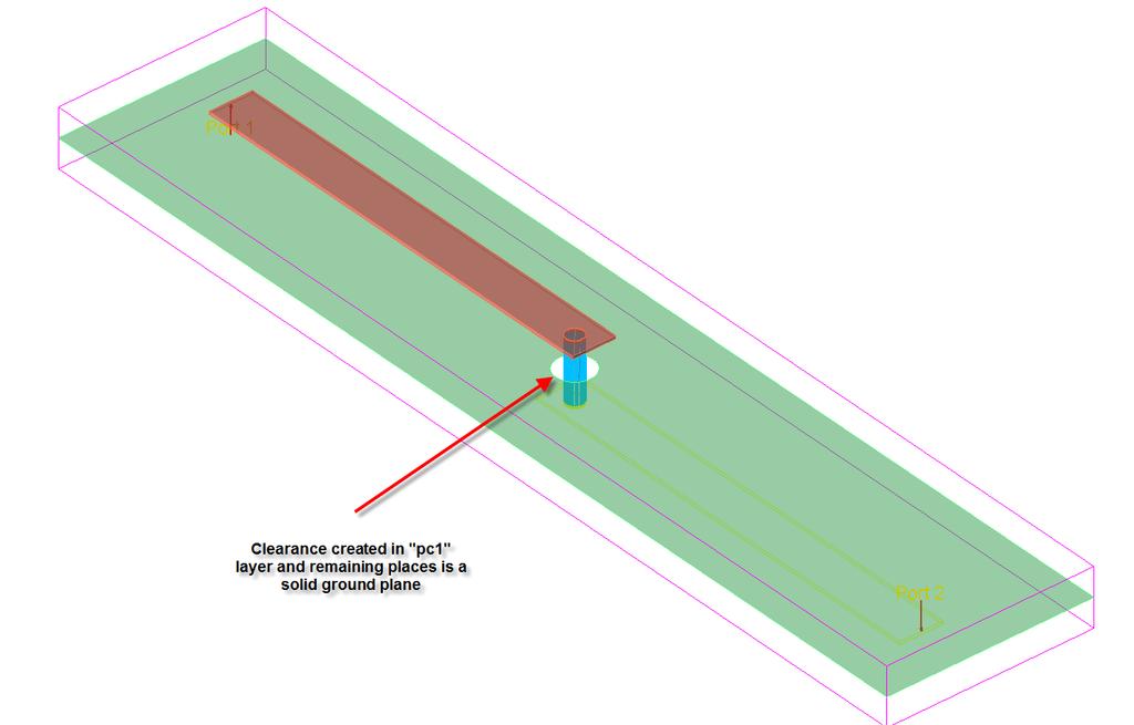
7 Example2: Line on cond and cond2 layers with interconnecting VIA and ground plane on pc1 layer Here is another example of lines on cond and cond2 layers interconnected by a VIA drawn on hole layer as per the stackup definition Snapshot with cond and cond2 layer switched off. Zoomed-In view of the VIA transition where the clearance was created in pc1 layer to avoid VIA getting shorted with ground plane on pc1 layer

8 Simulation and Results Comparison between STRIP and SLOT ground approach In order to compare results obtained by Finite Ground (Strip) or Slot ground approach, we shall run simulation on examples shown previously and results are summarized below. Care is taken to make sure simulation; mesh settings etc are kept common for respective cases Example1: Long Transmission Line We can notice here that responses are pretty comparable with very minor differences which may be due to the different formulations used for finite ground and Slot mode simulation approach but TDR showing impedance predicted is nearly the same so either mode of simulation should serve the purpose. Benefit of using SLOT mode for complex designs where lot of conductor is present on ground layers is that it saves significant amount of simulation time and memory requirements with minimal loss of accuracy and not to forget time spent on + & - Pin pairing for each Terminations.

9 Example2: Lines with Interconnecting VIA Again we can notice that responses agree pretty well for 2 nd case as well END OF DOCUMENT-----
Genesys 2012 Tutorial - Using Momentum Analysis for Microwave Planar Circuits
 Genesys 2012 Tutorial - Using Momentum Analysis for Microwave Planar Circuits Create the following schematics in Figure 1 with Genesys s schematic editor, which depicts two sections of a cascaded microstrip
Outline. Darren Wang ADS Momentum P2
 Outline Momentum Basics: Microstrip Meander Line Momentum RF Mode: RFIC Launch Designing with Momentum: Via Fed Patch Antenna Momentum Techniques: 3dB Splitter Look-alike Momentum Optimization: 3 GHz Band
LAB EXERCISE 2 EM Basics (Momentum)
") ADS 2012 EM Basics (v2 April 2013) LAB EXERCISE 2 EM Basics (Momentum) Topics: EM simulation in ADS, focusing on Momentum, including substrate and port setups, 3D viewing, visualization, and more. Audience:
ADS 2012 EM Basics (v2 April 2013) LAB EXERCISE 2 EM Basics (Momentum) Topics: EM simulation in ADS, focusing on Momentum, including substrate and port setups, 3D viewing, visualization, and more. Audience:
Microwave Office Training
 Microwave Office Training Schematic Layout Schematic Layout Schematic View Circuit We are Here! Schematic Layout View External World Need Export Mapping Two views of the same circuit! - including connectivity
AXIEM EM Simulation/Verification of a Cadence Allegro PCB
 Application Example AXIEM EM Simulation/Verification of a Cadence Allegro PCB Overview This application example outlines the electromagnetic (EM) simulation and verification flow that exists between Cadence
Layer Stackup Wizard: Intuitive Pre-Layout Design
 Application Brief Layer Stackup Wizard: Intuitive Pre-Layout Design INTRODUCTION This Application Brief describes the Layer Stackup Wizard, a powerful utility within ANSYS SIwave for pre-layout stackup
ECE ILLINOIS. ECE 451: Ansys HFSS Tutorial. Simulate and Analyze an Example of Microstrip Line. Drew Handler, Jerry Yang October 20, 2014
 ECE ILLINOIS ECE 451: Ansys HFSS Tutorial Simulate and Analyze an Example of Microstrip Line Drew Handler, Jerry Yang October 20, 2014 Introduction ANSYS HFSS is an industry standard tool for simulating
Laboratory Assignment: EM Numerical Modeling of a Stripline
 Laboratory Assignment: EM Numerical Modeling of a Stripline Names: Objective This laboratory experiment provides a hands-on tutorial for drafting up an electromagnetic structure (a stripline transmission
Using Sonnet in a Cadence Virtuoso Design Flow
 Using Sonnet in a Cadence Virtuoso Design Flow Purpose of this document: This document describes the Sonnet plug-in integration for the Cadence Virtuoso design flow, for silicon accurate EM modelling of
Ansoft HFSS 3D Boundary Manager
 and Selecting Objects and s Menu Functional and Ansoft HFSS Choose Setup / to: Define the location of ports, conductive surfaces, resistive surfaces, and radiation (or open) boundaries. Define sources
Chapter 4 Determining Cell Size
 Chapter 4 Determining Cell Size Chapter 4 Determining Cell Size The third tutorial is designed to give you a demonstration in using the Cell Size Calculator to obtain the optimal cell size for your circuit
Lab 1: Microstrip Line
 Lab 1: Microstrip Line In this lab, you will build a simple microstrip line to quickly familiarize yourself with the EMPro User Interface and how to setup FEM and FDTD simulations. If you are doing only
Powerful features (1)
") HFSS Overview Powerful features (1) Tangential Vector Finite Elements Provides only correct physical solutions with no spurious modes Transfinite Element Method Adaptive Meshing r E = t E γ i i ( x, y,
HFSS Overview Powerful features (1) Tangential Vector Finite Elements Provides only correct physical solutions with no spurious modes Transfinite Element Method Adaptive Meshing r E = t E γ i i ( x, y,
Keysight EEsof EDA Planar Electromagnetic (EM) Simulation in ADS. Demo Guide
 Simulation in ADS. Demo Guide") Keysight EEsof EDA Planar Electromagnetic (EM) Simulation in ADS Demo Guide 02 Keysight Planar Electromagnetic (EM) Simulation in ADS - Demo Guide Keysight ADS provides two key electromagnetic simulators
Keysight EEsof EDA Planar Electromagnetic (EM) Simulation in ADS Demo Guide 02 Keysight Planar Electromagnetic (EM) Simulation in ADS - Demo Guide Keysight ADS provides two key electromagnetic simulators
A Proposed Set of Specific Standard EMC Problems To Help Engineers Evaluate EMC Modeling Tools
 A Proposed Set of Specific Standard EMC Problems To Help Engineers Evaluate EMC Modeling Tools Bruce Archambeault, Ph. D Satish Pratapneni, Ph.D. David C. Wittwer, Ph. D Lauren Zhang, Ph.D. Juan Chen,
1/Build a Mintronics: MintDuino
 1/Build a Mintronics: The is perfect for anyone interested in learning (or teaching) the fundamentals of how micro controllers work. It will have you building your own micro controller from scratch on
An Introduction to the Finite Difference Time Domain (FDTD) Method & EMPIRE XCcel
 Method & EMPIRE XCcel") An Introduction to the Finite Difference Time Domain (FDTD) Method & EMPIRE XCcel Simulation Model definition for FDTD DUT Port Simulation Box Graded Mesh six Boundary Conditions 1 FDTD Basics: Field components
An Introduction to the Finite Difference Time Domain (FDTD) Method & EMPIRE XCcel Simulation Model definition for FDTD DUT Port Simulation Box Graded Mesh six Boundary Conditions 1 FDTD Basics: Field components
RF/Microwave Circuits I Laboratory #2. Circuit Tuning and EM Simulation with Momentum
 RF/Microwave Circuits I Laboratory #2 Circuit Tuning and EM Simulation with Momentum Overview This laboratory continues the basic ADS training approach from Laboratory #1. The two main objectives for this
EDA365. DesignCon Impact of Backplane Connector Pin Field on Trace Impedance and Vertical Field Crosstalk
 DesignCon 2007 Impact of Backplane Connector Pin Field on Trace Impedance and Vertical Field Crosstalk Ravi Kollipara, Rambus, Inc. ravik@rambus.com, (650) 947-5298 Ben Chia, Rambus, Inc. Dan Oh, Rambus,
SPEED2000 TDR/TDT Simulation Tutorial. Product Version 16.6 December 2012
 Product Version 16.6 December 2012 2012 Cadence Design Systems, Inc. All rights reserved. Cadence Design Systems, Inc. (Cadence), 2655 Seely Ave., San Jose, CA 95134, USA. Open SystemC, Open SystemC Initiative,
ELC 4383 RF/Microwave Circuits I Laboratory 5: Circuit Tuning and Electromagnetic Simulation
 1 ELC 4383 RF/Microwave Circuits I Laboratory 5: Circuit Tuning and Electromagnetic Simulation Note: This lab procedure has been adapted from a procedure written by Dr. Tom Weller at the University of
FEKO Tutorial I. Mohammad S. Sharawi, Ph.D. Electrical Engineering Department
 Mohammad S. Sharawi, Ph.D. Electrical Engineering Department This tutorial will get you started with FEKO. FEKO is a full-wave electromagnetic field simulator that is based on the Method of Moments (MoM).
Lesson 5: Board Design Files
 5 Lesson 5: Board Design Files Learning Objectives In this lesson you will: Use the Mechanical Symbol Editor to create a mechanical board symbol Use the PCB Design Editor to create a master board design
FEKO Tutorial II. Mohammad S. Sharawi, Ph.D. Electrical Engineering Department
 Mohammad S. Sharawi, Ph.D. Electrical Engineering Department This tutorial will get you started with FEKO. FEKO is a full-wave electromagnetic field simulator that is based on the Method of Moments (MoM).
EMPro Workshop. Version 4.0 Updated Feb, 2015
 EMPro Workshop Version 4.0 Updated Feb, 2015 Agenda Page 2 Introduction Getting started with the standalone EMPro EM simulation work flow with examples Getting started with EMPro 3D component work flow
Allegro PCB Editor with Performance Option or higher. The Reuse function can be used to create panels in PCB Editor
 Title: Product: Summary: Panelization with Reuse Allegro PCB Editor with Performance Option or higher The Reuse function can be used to create panels in PCB Editor Author/Date: Beate Wilke / 07.02.2011
m/matl - The EM Technology File Editor for RFIC
 m/matl - The EM Technology File Editor for RFIC Table of contents: m/matl - The EM Technology File Editor for RFIC... 1 1. Introduction... 2 2. What file formats and design flows are supported?... 2 Read
TQPED MMIC Design Training
 TQPED MMIC Design Training Outline Installation and Use of the Library AWR AWR Design Kit (PDK Process Design Kit) ICED Layout Kit Create a new document using the Library Environment Setup Hotkeys Background
Digitizer Leapfrogging
 Digitizer Leapfrogging Leapfrogging lets you digitize objects that are larger than your digitizing arm. You start with one section of the object, then leapfrog around by creating leapfrog stations in both
Vertical Launch Connectors
 Microwave Farm s are specially designed for solderless vertical PCB launch on test & measurement board. These connectors have excellent electrical transition performance up to 26.5 GHz, 40 GHz,50 GHz &
Note. The above image and many others are courtesy of - this is a wonderful resource for designing circuits.
 Robotics and Electronics Unit 2. Arduino Objectives. Students will understand the basic characteristics of an Arduino Uno microcontroller. understand the basic structure of an Arduino program. know how
A Crash Course on Using Agilent Advanced Design System (ADS)
") A Crash Course on Using Agilent Advanced Design System (ADS) By Chris Sanabria, sanabria@ece.ucsb.edu 2/9/02 If you are an engineer and have anything to do with circuit simulation, in particular high frequency
A Crash Course on Using Agilent Advanced Design System (ADS) By Chris Sanabria, sanabria@ece.ucsb.edu 2/9/02 If you are an engineer and have anything to do with circuit simulation, in particular high frequency
LAB EXERCISE 3B EM Techniques (Momentum)
") ADS 2012 EM Basics (v2 April 2013) LAB EXERCISE 3B EM Techniques (Momentum) Topics: EM options for meshing and the preprocessor, and using EM to simulate an inductor and use the model in schematic. Audience:
ADS 2012 EM Basics (v2 April 2013) LAB EXERCISE 3B EM Techniques (Momentum) Topics: EM options for meshing and the preprocessor, and using EM to simulate an inductor and use the model in schematic. Audience:
Efficient Meshing in Sonnet
 Efficient Meshing in Sonnet Purpose of this document: In this document, we will discuss efficient meshing in Sonnet, based on a wide variety of application examples. It will be shown how manual changes
Contents Contents Creating a Simulation Example: A Dipole Antenna AMDS User s Guide
 Contents Contents 1 Creating a Simulation 7 Introduction 8 Data Files for Examples 8 Software Organization 9 Constructing the Geometry 10 Creating the Mesh 11 Defining Run Parameters 13 Requesting Results
Lesson 13: The Graph of a Linear Equation in Two Variables
 Student Outcomes Students predict the shape of a graph of a linear equation by finding and plotting solutions on a coordinate plane. Students informally explain why the graph of a linear equation is not
Basic User Manual Maxwell 2D Student Version. Rick Hoadley Jan 2005
 1 Basic User Manual Maxwell 2D Student Version Rick Hoadley Jan 2005 2 Overview Maxwell 2D is a program that can be used to visualize magnetic fields and predict magnetic forces. Magnetic circuits are
Especially, for Flex-Rigid design, the designer can add sub layer stack for different board regions.
 Layer Stack Manager Old Content - visit altium.com/documentation Modified by Annika Krilov on 14-Jul-2015 Parent page: PCB Dialogs The Layer Stack Manager(Flex-Rigid) Dialog. Summary The Layer Stack Manager
Optimum Placement of Decoupling Capacitors on Packages and Printed Circuit Boards Under the Guidance of Electromagnetic Field Simulation
 Optimum Placement of Decoupling Capacitors on Packages and Printed Circuit Boards Under the Guidance of Electromagnetic Field Simulation Yuzhe Chen, Zhaoqing Chen and Jiayuan Fang Department of Electrical
Workshop 3-1: Coax-Microstrip Transition
 Workshop 3-1: Coax-Microstrip Transition 2015.0 Release Introduction to ANSYS HFSS 1 2015 ANSYS, Inc. Example Coax to Microstrip Transition Analysis of a Microstrip Transmission Line with SMA Edge Connector
Sonnet is based in Syracuse, NY, USA with representatives across the globe.
 Getting Started At Sonnet, we've been developing 3D planar high frequency EM software since 1983, and our software has earned a solid reputation as the world's most accurate commercial planar EM analysis
Vertical Launch Connectors
 Microwave Farm s Vertical Launch Connectors are specially designed for solderless vertical PCB launch on test & measurement board. These connectors have excellent electrical transition performance up to
Autodesk Fusion 360: Model. Overview. Modeling techniques in Fusion 360
 Overview Modeling techniques in Fusion 360 Modeling in Fusion 360 is quite a different experience from how you would model in conventional history-based CAD software. Some users have expressed that it
Large Solderable Breadboard Hookup Guide
 Page 1 of 5 Large Solderable Breadboard Hookup Guide Introduction Solderless breadboards are great for prototyping. But they re not exactly mechanically robust. It seems like something, somewhere is always
Probe Card Crosstalk: How to Control the RF Fields
 Probe Card Crosstalk: How to Control the RF Fields Daniel Bock, Ph.D RF Applications Product Specialist Form Factor Ebenezer Odu RF Test Engineer Qorvo Agenda 1. Overview 2. What is Crosstalk 1. Impact
Porsche 91 1GT D m o d e ling tutorial - by Nim
 orsche 911GT 3D modeling tutorial - by Nimish In this tutorial you will learn to model a car using Spline modeling method. This method is not very much famous as it requires considerable amount of skill
Agilent Electromagnetic Design System
 Agilent 85270 Electromagnetic Design System Getting Started Agilent Technologies Notices Agilent Technologies, Inc. 2006 No part of this manual may be reproduced in any form or by any means (including
Animation is the illusion of motion created by the consecutive display of images of static elements. In film and video
 Class: Name: Class Number: Date: Computer Animation Basis A. What is Animation? Animation is the illusion of motion created by the consecutive display of images of static elements. In film and video production,
Electronic Coin Toss
 1 Electronic Coin Toss Why this circuit? This circuit was not designed for people who can make up their mind nor have a coin to use for a heads or tail coin toss. This circuit can also be used to ask it
EXAMINING THE IMPACT OF SPLIT PLANES ON SIGNAL AND POWER INTEGRITY
 EXAMINING THE IMPACT OF SPLIT PLANES ON SIGNAL AND POWER INTEGRITY Jason R. Miller, Gustavo J. Blando, Roger Dame, K. Barry A. Williams and Istvan Novak Sun Microsystems, Burlington, MA 1 AGENDA Introduction
Using Sonnet Interface in Eagleware-Elanix GENESYS. Sonnet Application Note: SAN-205A JULY 2005
 Using Sonnet Interface in Eagleware-Elanix GENESYS Sonnet Application Note: SAN-205A JULY 2005 Description of Sonnet Suites Professional Sonnet Suites Professional is an industry leading full-wave 3D Planar
Integrating ADS into a High Speed Package Design Process
 Integrating ADS into a High Speed Package Design Process Page 1 Group/Presentation Title Agilent Restricted Month ##, 200X Agenda High Speed SERDES Package Design Requirements Performance Factor and Design
Welcome. Joe Civello ADS Product Manager Agilent Technologies
 Welcome Joe Civello ADS Product Manager Agilent Technologies Agilent Technologies 2011 Agenda RF & microwave market trends & how Agilent EEsof is investing its R&D Multi-technology design with ADS 2011
I N T E R C O N N E C T A P P L I C A T I O N N O T E. STRADA Whisper 4.5mm Connector Enhanced Backplane and Daughtercard Footprint Routing Guide
 I N T E R C O N N E C T A P P L I C A T I O N N O T E STRADA Whisper 4.5mm Connector Enhanced Backplane and Daughtercard Footprint Routing Guide Report # 32GC001 01/26/2015 Rev 3.0 STRADA Whisper Connector
Large-Scale Full-Wave Simulation
 Large-Scale Full-Wave Simulation Sharad Kapur and David Long Integrand Software, Inc. Areas of interest Consistent trends in IC design Increasing operating frequencies Modeling of passive structures (components,
HFSS 14 Update for SI and RF Applications Markus Kopp Product Manager, Electronics ANSYS, Inc.
 HFSS 14 Update for SI and RF Applications Markus Kopp Product Manager, Electronics ANSYS, Inc. 1 ANSYS, Inc. September 21, Advanced Solvers: Finite Arrays with DDM 2 ANSYS, Inc. September 21, Finite Arrays
Antenna-Simulation of a Half-wave Dielectric Resonator filter
 Antenna-Simulation of a Half-wave Dielectric Resonator filter 1. Description A symmetric model of a dielectric resonator filter is analyzed using the Scattering parameters module of HFWorks to determine
MAGIC TUTORIAL. Getting Started: Background Info: RLW 10/15/98 3:12 PM
 MAGIC TUTORIAL Getting Started: Login to one of the workstations located in ECEE 253 using login name iclab. There is no password so just hit [enter]. The local directory on each machine is /home/sp98/iclab.
EFFECTIVE PEEC MODELING OF TRANSMISSION LINES STRUCTURES USING A SELECTIVE MESH APPROACH
 EFFECTIVE PEEC MODELING OF TRANSMISSION LINES STRUCTURES USING A SELECTIVE MESH APPROACH A.B Gurulakshmi 1 and Dr. N. Suresh Kumar 2 1 Department of Electronics and Communication Engineering,Vickram College
CECOS University Department of Electrical Engineering. Wave Propagation and Antennas LAB # 1
 CECOS University Department of Electrical Engineering Wave Propagation and Antennas LAB # 1 Introduction to HFSS 3D Modeling, Properties, Commands & Attributes Lab Instructor: Amjad Iqbal 1. What is HFSS?
Sherlock Tutorial Project Overview
 Sherlock Tutorial Project Overview Background Sherlock organizes design files, inputs and analysis results as project folders that can be managed inside of the Sherlock application and shared between Sherlock
Chapter 7 Agilent Interface Tutorial
 Chapter 7 Agilent Interface Tutorial Chapter 7 Agilent Interface Tutorial This tutorial provides you with an overview of the basic use of the Agilent Interface. For a detailed discussion of the Agilent
Recent Via Modeling Methods for Multi-Vias in a Shared Anti-pad
 Recent Via Modeling Methods for Multi-Vias in a Shared Anti-pad Yao-Jiang Zhang, Jun Fan and James L. Drewniak Electromagnetic Compatibility (EMC) Laboratory, Missouri University of Science &Technology
Ansoft HFSS Version 7 Training Section 5: Boundary Module
 Ansoft HFSS Version 7 Training Section 5: Boundary Module 5-1 General Overview Synopsis Boundary Types, Definitions, and Parameters Source Types, Definitions, and Parameters Interface Layout Assigning
Maxwell 2D Student Version. A 2D Electrostatic Problem
 Maxwell 2D Student Version A 2D Electrostatic Problem November 2002 Notice The information contained in this document is subject to change without notice. Ansoft makes no warranty of any kind with regard
IMPLEMENTATION OF ANALYTICAL (MATLAB) AND NUMERICAL (HFSS) SOLUTIONS ADVANCED ELECTROMAGNETIC THEORY SOHAIB SAADAT AFRIDI HAMMAD BUTT ZUNNURAIN AHMAD
 AND NUMERICAL (HFSS) SOLUTIONS ADVANCED ELECTROMAGNETIC THEORY SOHAIB SAADAT AFRIDI HAMMAD BUTT ZUNNURAIN AHMAD") STUDY OF SCATTERING & RESULTANT RADIATION PATTERN: INFINITE LINE CURRENT SOURCE POSITIONED HORIZONTALLY OVER A PERFECTLY CONDUCTING INFINITE GROUND PLANE IMPLEMENTATION OF ANALYTICAL (MATLAB) AND NUMERICAL
STUDY OF SCATTERING & RESULTANT RADIATION PATTERN: INFINITE LINE CURRENT SOURCE POSITIONED HORIZONTALLY OVER A PERFECTLY CONDUCTING INFINITE GROUND PLANE IMPLEMENTATION OF ANALYTICAL (MATLAB) AND NUMERICAL
Release Highlights for BluePrint-PCB Product Version 2.2.2
 Release Highlights for BluePrint-PCB Product Version 2.2.2 Introduction BluePrint V2.2.2 Build 512 is a rolling release. Rolling releases enable us to provide enhancements and defect fixes to the market
Quick Tips to Using I-DEAS. Learn about:
 Learn about: Quick Tips to Using I-DEAS I-DEAS Tutorials: Fundamental Skills windows mouse buttons applications and tasks menus icons part modeling viewing selecting data management using the online tutorials
Excel 2013 Intermediate
 Instructor s Excel 2013 Tutorial 2 - Charts Excel 2013 Intermediate 103-124 Unit 2 - Charts Quick Links Chart Concepts Page EX197 EX199 EX200 Selecting Source Data Pages EX198 EX234 EX237 Creating a Chart
Ansys Designer RF Training Lecture 2: Introduction to the Designer GUI
 Ansys Designer RF Solutions for RF/Microwave Component and System Design 7. 0 Release Ansys Designer RF Training Lecture 2: Introduction to the Designer GUI Ansoft Designer Desktop Menu bar Toolbars Schematic
Bold is used for UI elements that will appear on screen (buttons, menus or menu items, etc.)
") PCB Workshop Notes 26 November 2015 Tutorial References (presentation, sample project): http://ieee.concordia.ca/portfolio/pcb workshop/ Vocabulary & Concepts Software: DipTrace, in this case Packages:
PCB Workshop Notes 26 November 2015 Tutorial References (presentation, sample project): http://ieee.concordia.ca/portfolio/pcb workshop/ Vocabulary & Concepts Software: DipTrace, in this case Packages:
Dynamic Blocks in AutoCAD 2006
 AutoCAD 2006 Dynamic Blocks in AutoCAD 2006 Part 1 of 3: Dynamic Block Overview and Quick-Start Tutorial In AutoCAD 2006 software, you can now create blocks that are intelligent and flexible. This exciting
SOLIDWORKS: Lesson III Patterns & Mirrors. UCF Engineering
 SOLIDWORKS: Lesson III Patterns & Mirrors UCF Engineering Solidworks Review Last lesson we discussed several more features that can be added to models in order to increase their complexity. We are now
High-Speed Layout Guidelines for Reducing EMI for LVDS SerDes Designs. I.K. Anyiam
 High-Speed Layout Guidelines for Reducing EMI for LVDS SerDes Designs I.K. Anyiam 1 Introduction LVDS SerDes helps to reduce radiated emissions, but does not completely eliminate them EMI prevention must
Topic. Section 4.1 (3, 4)
") Topic.. California Standards: 6.0: Students graph a linear equation and compute the x- and y-intercepts (e.g., graph x + 6y = ). They are also able to sketch the region defined by linear inequality (e.g.,
Topic.. California Standards: 6.0: Students graph a linear equation and compute the x- and y-intercepts (e.g., graph x + 6y = ). They are also able to sketch the region defined by linear inequality (e.g.,
Agilent W2100 Antenna Modeling Design System
 Agilent W2100 Antenna Modeling Design System User s Guide Agilent Technologies Notices Agilent Technologies, Inc. 2007 No part of this manual may be reproduced in any form or by any means (including electronic
ROTOPOD PERISCOPE LIGHTING KIT
 ROTOPOD PERISCOPE LIGHTING KIT (for ULTIMATE Periscopes) 14-MAR-2013_rev 2.0 I designed the Periscope Lighting Kit to be as flexible as possible. Every LED is individually controllable. I have provided
EEC 134 RF/MICROWAVE DESIGN-WINTER 2017 Professor. Xiaoguang Leo Liu Team TEAM Lap Hoang RF System Design on KiCad and Soldering
 EEC 134 RF/MICROWAVE DESIGN-WINTER 2017 Professor. Xiaoguang Leo Liu Team TEAM Lap Hoang RF System Design on KiCad and Soldering Abstract This paper presents the process of how we transform our RF system
Polygon Pours and Copper Regions. Fills and Solid Regions. Modified by Admin on Nov 18, 2013
 Polygon Pours and Copper Regions Old Content - visit altium.com/documentation Modified by Admin on Nov 18, 2013 A common requirement on a printed circuit board is large areas of copper. It could be a hatched
UV Mapping to avoid texture flaws and enable proper shading
 UV Mapping to avoid texture flaws and enable proper shading Foreword: Throughout this tutorial I am going to be using Maya s built in UV Mapping utility, which I am going to base my projections on individual
Keysight EEsof EDA EMPro
 Keysight EEsof EDA EMPro 3D Electromagnetic Modeling and Simulation Environment Integrated with your ADS Design Flow Brochure Introduction Electromagnetic Professional (EMPro) is a 3D modeling and simulation
Chip/Package/Board Design Flow
 Chip/Package/Board Design Flow EM Simulation Advances in ADS 2011.10 1 EM Simulation Advances in ADS2011.10 Agilent EEsof Chip/Package/Board Design Flow 2 RF Chip/Package/Board Design Industry Trends Increasing
Connecting LEDs to the ADB I/O
 Application Note AN-2 By Magnus Pettersson September 26 1996 Connecting LEDs to the I/O Introduction The following notes are for those of you who are a bit inexperienced with hardware components. This
Design rule illustrations for the AMI C5N process can be found at:
 Cadence Tutorial B: Layout, DRC, Extraction, and LVS Created for the MSU VLSI program by Professor A. Mason and the AMSaC lab group. Revised by C Young & Waqar A Qureshi -FS08 Document Contents Introduction
CONTENTS Preface Introduction Finite Element Formulation Finite Element Mesh Truncation
 Preface xi 1 Introduction 1 1.1 Numerical Simulation of Antennas 1 1.2 Finite Element Analysis Versus Other Numerical Methods 2 1.3 Frequency- Versus Time-Domain Simulations 5 1.4 Brief Review of Past
A Quick EAGLE PCB Tutorial
 A Quick EAGLE PCB Tutorial Tim Steffes Mark Brehob 9/17/11 Introduction So, you ve finished your circuit prototype and you re ready to make it permanent? Tired of those messy wires and loose components,
Release Notes Version 5
 Release Notes Version 5 Version 5.1 (2017-01-31) Solder Joint Fatigue Calculix Support for Column Grid Array (CGA) modeling for Solder Joint Fatigue FEA analysis and the Solder Fatigue tool has been added
Modeling of Connector to PCB Interfaces. CST User Group Meeting, September 14, 2007 Thomas Gneiting, AdMOS GmbH
 Modeling of Connector to PCB Interfaces CST User Group Meeting, September 14, 2007 Thomas Gneiting, AdMOS GmbH thomas.gneiting@admos.de Table of Content Introduction Parametric CST model of connector to
Creating Vector Shapes Week 2 Assignment 1. Illustrator Defaults
 Illustrator Defaults Before we begin, we are going to make sure that all of us are using the same settings within our application. For this class, we will always want to make sure that our application
Sorting Through EM Simulators
 DesignFeature DAVE MORRIS Application Engineer Agilent Technologies, Lakeside, Cheadle Royal Business Park, Stockport 3K8 3GR, England; e-mail: david_morris@agilent.com, www.agilent.com. ELECTRONICALLY
Autodesk Inventor : From Concept to Digital Prototype
 Autodesk Inventor : From Concept to Digital Prototype Bryan Fields Advanced Solutions, Inc. MA305-5 Using the tools available in Autodesk Inventor, this session will look at the progression from concept
Skill Development Centre by AN ISO CERTIFIED COMPANY
 Skill Development Centre by AN ISO CERTIFIED COMPANY Industrial Automation Training Embedded/ VLSI system design Electrical control panel Design Product Development Fiber optics Technician Electrician
Process technology and introduction to physical
 Neuromorphic Engineering II Lab 3, Spring 2014 1 Lab 3 March 10, 2014 Process technology and introduction to physical layout Today you will start to learn to use the Virtuoso layout editor XL which is
Package on Board Simulation with 3-D Electromagnetic Simulation
 White Paper Package on Board Simulation with 3-D Electromagnetic Simulation For many years, designers have taken into account the effect of package parasitics in simulation, from using simple first-order
CS755 CAD TOOL TUTORIAL
 CS755 CAD TOOL TUTORIAL CREATING SCHEMATIC IN CADENCE Shi-Ting Zhou shi-ting@cs.wisc.edu After you have figured out what you want to design, and drafted some pictures and diagrams, it s time to input schematics
CHAPTER 6 MICROSTRIP RECTANGULAR PATCH ARRAY WITH FINITE GROUND PLANE EFFECTS
 107 CHAPTER 6 MICROSTRIP RECTANGULAR PATCH ARRAY WITH FINITE GROUND PLANE EFFECTS 6.1 INTRODUCTION The finite ground plane effects of microstrip antennas are one of the issues for the wireless mobile communication
HFSS: Optimal Phased Array Modeling Using Domain Decomposition
 HFSS: Optimal Phased Array Modeling Using Domain Decomposition 15. 0 Release Authors: Dane Thompson Nick Hirth Irina Gordion Sara Louie Presenter: Dane Thompson Motivation Electronically scannable antenna
Alphabetic Key Word Catalogue for PUFF 2.1
 Alphabetic Key Word Catalogue for PUFF 2.1 Key Word Commands / key combinations Break port connection to circuit Press F1. Position the cursor on appropriate connection point of a port in circuit and then
Using PSpice to Simulate Transmission Lines K. A. Connor Summer 2000 Fields and Waves I
 Using PSpice to Simulate Transmission Lines K. A. Connor Summer 2000 Fields and Waves I We want to produce the image shown above as a screen capture or below as the schematic of this circuit. R1 V1 25
Si8000m Version History
 Si8000m Version History Si8000m Key product milestones (Detailed change history on following pages) 2019 New Monte Carlo Analysis option Updated bi-directional copy / paste interface between Speedstack