Workshop on Digital Circuit Design in FPGA
|
|
|
- Annis McBride
- 5 years ago
- Views:
Transcription


1 Workshop on Digital Circuit Design in FPGA Session-1 Presented By Mohammed Abdul Kader Assistant Professor, Dept. of EEE, IIUC Website: kader05cuet.wordpress.com
2 The field-programmable gate array (FPGA) is a semiconductor device that can be programmed after manufacturing. Instead of being restricted to any predetermined hardware function, an FPGA allows you to program product features and functions, adapt to new standards, and reconfigure hardware for specific applications even after the product has been installed in the field hence the name "field-programmable". You can use an FPGA to implement any logical function that an application-specific integrated circuit (ASIC) or, application-specific standard product (ASSP) could perform, but the ability to update the functionality after shipping offers advantages for many applications. What is an FPGA?

3 FPGA Architecture IOB Input/Output Block. CLB Configurable Logic Block. PSM Programmable Switch Matrix. Connection Lines Clock Circuitry 3


4 FPGA Vs Microcontroller Microcontroller: Micro-computer in a single chip. Configuring a predefined hardware by programming. FPGA: Developing Hardware by programming 4
5 FPGA Programming FPGA Programming Schematic Entry Hardware Description language Verilog HDL VHDL RTL Verilog Code Structural Verilog Code Behavioral Verilog Code 5
6 Schematic Design in FPGA Implementation of Full adder circuit X Y S = X Y Z Z C = Z(X Y) + XY Steps: a) Open a new project Wizard. b) Open a new schematic file. c) Draw the circuit. d) Compilation. e) Pin Planer. f) Compilation g) Upload 6

7 Open a new project Wizard. Schematic Design in FPGA(Cont.)

8 Family and Device Settings Schematic Design in FPGA(Cont.) 8

9 Drawing circuit in New Schematic File Schematic Design in FPGA(Cont.)

10 Pin Planner Schematic Design in FPGA(Cont.)

11 Loading Program Schematic Design in FPGA(Cont.) 11
12 Verilog HDL Structural Verilog Code
13 Verilog HDL Structural Verilog Code
14 Verilog HDL RTL Verilog Code RTL Verilog Coding of Digital Circuit Structural Verilog code is not practicable for designing complex circuit. In that case, RTL Verilog code is used to design digital circuit. RTL Verilog code of a digital design can be written in two ways: 1) Using continuous assignment structures. 2) Using Procedural assignment structures. Continuous assignment Vs Procedural assignment It is named as continuous assignment because the assignments written in this procedure are evaluated continuously whereas in procedural assignment structure execution of a statement waits for the clock or other parameter. The expression (in continuous assignment structure) is evaluated whenever any of the operands changes. RTL coding using continuous assignment is usually used to model combinational circuit which is more complex than can be handled by structural modeling. The declaration module, input, output and endmodule are same as they are used in structural Verilog code. The difference is the keyword assign is used to write the continuous assignment. 14
15 RTL Verilog Code using Continuous Assignment RTL Verilog code using Continuous Assignment to follow the logic equations given below. Verilog Code: 15
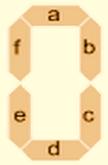
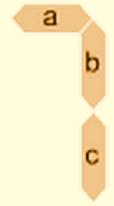
16 RTL Verilog Code using Continuous Assignment BCD to Seven Segment Decoder by RTL Verilog Coding using Continuous assignment A BCD to seven-segment decoder is a combinational circuit that accepts a decimal digit in BCD and generates the appropriate outputs for the selection of segments in a display indicator used for displaying the decimal digit. The seven output of the decoder (a,b,c,d,e,f,g) select the corresponding segments in the display as shown in figure a. The numeric designation chosen to represent the decimal digit is shown in figure b. Design the BCD to seven segment decoder circuit. a: Segment designation b: Numerical designation for display 16

 110101 101010")


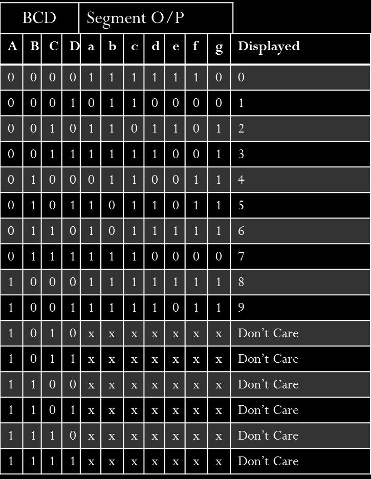
17 RTL Verilog Code using Continuous Assignment (Cont.) From truth table we obtaineda= (0,2,3,5,6,7,8,9) b= (0,1,2,3,4,7,8,9) c= (0,1,3,4,5,6,7,8,9) d= (0,2,3,5,6,8,9) e= (0,2,6,8) f= (0,4,5,6,8,9) g= (2,3,4,5,6,8,9) Don t care conditions, d= (10,11,12,13,14,15) 17
 b=")
 d=")
 g= (2,3,4,5,6,8,9)")


18 From truth table we obtaineda= (0,2,3,5,6,7,8,9) b= (0,1,2,3,4,7,8,9) c= (0,1,3,4,5,6,7,8,9) d= (0,2,3,5,6,8,9) e= (0,2,6,8) f= (0,4,5,6,8,9) g= (2,3,4,5,6,8,9) Don t care, d= (10,11,12,13,14,15) CD AB CD AB CD CD AB AB RTL Verilog Code using Continuous Assignment (Cont.) X X X X X X X X X X X X X X X X X X X X X X X X AB a= A+C+B D +BD CD AB b= B +C D +CD c= B +C +D d= A +B D +B C+BC D+CD CD CD AB 18 X X X X X X X X X X X X X X X X X X e= B D +CD f= A+C D +BD +BC g= A+B C+BC +BD
19 RTL Verilog Code using Continuous Assignment (Cont.) Logic Equations a= A+C+B D +BD b= B +C D +CD c= B +C +D d= A +B D +B C+BC D+CD e= B D +CD f= A+C D +BD +BC g= A+B C+BC +BD Verilog Code module seven_segment (a,b,c,d,e,f,g,a,b,c,d); input A,B,C,D; output a,b,c,d,e,f,g; assign a=a C (~B&~D) (B&D); assign b=(~b (~C&~D) (C&D)); assign c=b ~C D; assign d=a (~B&~D) (~B&C) (B&~C&D) (C&~D); assign e=(~b&~d) (C&~D); assign f=a (~C&~D) (B&~D) (B&~C); assign g=a (~B&C) (B&~C) (B&~D); endmodule 19
20 RTL Verilog Code using Continuous Assignment (Cont.) Verilog code to design 4-bit adder-subtractor circuit using continuous assignment structure. Verilog Code: 20
Workshop on Digital Circuit Design in FPGA
 Organized by: Dept. of EEE Workshop on Digital Circuit Design in FPGA Presented By Mohammed Abdul Kader Assistant Professor, Dept. of EEE, IIUC Email:kader05cuet@gmail.com Website: kader05cuet.wordpress.com
Hardware Description Languages (HDLs) Verilog
 Verilog") Hardware Description Languages (HDLs) Verilog Material from Mano & Ciletti book By Kurtulus KULLU Ankara University What are HDLs? A Hardware Description Language resembles a programming language specifically
Hardware Description Languages (HDLs) Verilog Material from Mano & Ciletti book By Kurtulus KULLU Ankara University What are HDLs? A Hardware Description Language resembles a programming language specifically
Fig. 6-1 Conventional and Array Logic Symbols for OR Gate
 6- (a) Conventional symbol (b) Array logic symbol Fig. 6- Conventional and Array Logic Symbols for OR Gate 2 Prentice Hall, Inc. 6-2 k address lines Read n data input lines emory unit 2 k words n bits
CHAPTER 9 MULTIPLEXERS, DECODERS, AND PROGRAMMABLE LOGIC DEVICES
 CHAPTER 9 MULTIPLEXERS, DECODERS, AND PROGRAMMABLE LOGIC DEVICES This chapter in the book includes: Objectives Study Guide 9.1 Introduction 9.2 Multiplexers 9.3 Three-State Buffers 9.4 Decoders and Encoders
Simplification of Boolean Functions
 Simplification of Boolean Functions Contents: Why simplification? The Map Method Two, Three, Four and Five variable Maps. Simplification of two, three, four and five variable Boolean function by Map method.
Code No: R Set No. 1
 Code No: R059210504 Set No. 1 II B.Tech I Semester Supplementary Examinations, February 2007 DIGITAL LOGIC DESIGN ( Common to Computer Science & Engineering, Information Technology and Computer Science
EE 8351 Digital Logic Circuits Ms.J.Jayaudhaya, ASP/EEE
 EE 8351 Digital Logic Circuits Ms.J.Jayaudhaya, ASP/EEE 1 Logic circuits for digital systems may be combinational or sequential. A combinational circuit consists of input variables, logic gates, and output
Combinational Logic Circuits
 Combinational Logic Circuits By Dr. M. Hebaishy Digital Logic Design Ch- Rem.!) Types of Logic Circuits Combinational Logic Memoryless Outputs determined by current values of inputs Sequential Logic Has
Combinational Logic. Prof. Wangrok Oh. Dept. of Information Communications Eng. Chungnam National University. Prof. Wangrok Oh(CNU) 1 / 93
 1 / 93") Combinational Logic Prof. Wangrok Oh Dept. of Information Communications Eng. Chungnam National University Prof. Wangrok Oh(CNU) / 93 Overview Introduction 2 Combinational Circuits 3 Analysis Procedure
Combinational Logic Prof. Wangrok Oh Dept. of Information Communications Eng. Chungnam National University Prof. Wangrok Oh(CNU) / 93 Overview Introduction 2 Combinational Circuits 3 Analysis Procedure
Boolean Logic CS.352.F12
 Boolean Logic CS.352.F12 Boolean Algebra Boolean Algebra Mathematical system used to manipulate logic equations. Boolean: deals with binary values (True/False, yes/no, on/off, 1/0) Algebra: set of operations
Code No: R Set No. 1
 Code No: R059210504 Set No. 1 II B.Tech I Semester Regular Examinations, November 2006 DIGITAL LOGIC DESIGN ( Common to Computer Science & Engineering, Information Technology and Computer Science & Systems
FPGA Design Challenge :Techkriti 14 Digital Design using Verilog Part 1
 FPGA Design Challenge :Techkriti 14 Digital Design using Verilog Part 1 Anurag Dwivedi Digital Design : Bottom Up Approach Basic Block - Gates Digital Design : Bottom Up Approach Gates -> Flip Flops Digital
EE 231 Fall Lab 1: Introduction to Verilog HDL and Altera IDE
 Lab 1: Introduction to Verilog HDL and Altera IDE Introduction In this lab you will design simple circuits by programming the Field-Programmable Gate Array (FPGA). At the end of the lab you should be able
Programmable Logic Devices HDL-Based Design Flows CMPE 415
 HDL-Based Design Flows: ASIC Toward the end of the 80s, it became difficult to use schematic-based ASIC flows to deal with the size and complexity of >5K or more gates. HDLs were introduced to deal with
DKT 122/3 DIGITAL SYSTEM 1
 Company LOGO DKT 122/3 DIGITAL SYSTEM 1 BOOLEAN ALGEBRA (PART 2) Boolean Algebra Contents Boolean Operations & Expression Laws & Rules of Boolean algebra DeMorgan s Theorems Boolean analysis of logic circuits
Chap.3 3. Chap reduces the complexity required to represent the schematic diagram of a circuit Library
 3.1 Combinational Circuits 2 Chap 3. logic circuits for digital systems: combinational vs sequential Combinational Logic Design Combinational Circuit (Chap 3) outputs are determined by the present applied
I 4 I 3 I 2 I 1 I 0 A 7 A 6 A 5 A 4 A 3 A 2 A 1 A 0 T-125. ROM Truth Table (Partial) 1997 by Prentice-Hall, Inc.
 1997 by Prentice-Hall, Inc.") 997 by Prentice-Hall, Inc. ano & Kime Upper Saddle River, New Jersey 7458 T-5 Inputs Outputs I 4 I 3 I I I A 7 A 6 A 5 A 4 A 3 A A A...... RO Truth Table (Partial) 997 by Prentice-Hall, Inc. ano & Kime
997 by Prentice-Hall, Inc. ano & Kime Upper Saddle River, New Jersey 7458 T-5 Inputs Outputs I 4 I 3 I I I A 7 A 6 A 5 A 4 A 3 A A A...... RO Truth Table (Partial) 997 by Prentice-Hall, Inc. ano & Kime
EE 231 Fall EE 231 Lab 3
 EE 231 Lab 3 Decoders and Multiplexers Decoders and multiplexers are important combinational circuits in many logic designs. Decoders convert n inputs to a maximum of unique 2 n outputs. A special case
Gate-Level Minimization
 Gate-Level Minimization ( 范倫達 ), Ph. D. Department of Computer Science National Chiao Tung University Taiwan, R.O.C. Fall, 2017 ldvan@cs.nctu.edu.tw http://www.cs.nctu.edu.tw/~ldvan/ Outlines The Map Method
Combinational Logic with MSI and LSI
 1010101010101010101010101010101010101010101010101010101010101010101010101010101010 1010101010101010101010101010101010101010101010101010101010101010101010101010101010 1010101010101010101010101010101010101010101010101010101010101010101010101010101010
NH 67, Karur Trichy Highways, Puliyur C.F, Karur District DEPARTMENT OF INFORMATION TECHNOLOGY CS 2202 DIGITAL PRINCIPLES AND SYSTEM DESIGN
 NH 67, Karur Trichy Highways, Puliyur C.F, 639 114 Karur District DEPARTMENT OF INFORMATION TECHNOLOGY CS 2202 DIGITAL PRINCIPLES AND SYSTEM DESIGN UNIT 2 COMBINATIONAL LOGIC Combinational circuits Analysis
VALLIAMMAI ENGINEERING COLLEGE. SRM Nagar, Kattankulathur DEPARTMENT OF ELECTRONICS AND COMMUNICATION ENGINEERING EC6302 DIGITAL ELECTRONICS
 VALLIAMMAI ENGINEERING COLLEGE SRM Nagar, Kattankulathur-603 203 DEPARTMENT OF ELECTRONICS AND COMMUNICATION ENGINEERING EC6302 DIGITAL ELECTRONICS YEAR / SEMESTER: II / III ACADEMIC YEAR: 2015-2016 (ODD
 UNIT II - COMBINATIONAL LOGIC Part A 2 Marks. 1. Define Combinational circuit A combinational circuit consist of logic gates whose outputs at anytime are determined directly from the present combination
Verilog Fundamentals. Shubham Singh. Junior Undergrad. Electrical Engineering
 Verilog Fundamentals Shubham Singh Junior Undergrad. Electrical Engineering VERILOG FUNDAMENTALS HDLs HISTORY HOW FPGA & VERILOG ARE RELATED CODING IN VERILOG HDLs HISTORY HDL HARDWARE DESCRIPTION LANGUAGE
CSCI 220: Computer Architecture I Instructor: Pranava K. Jha. Simplification of Boolean Functions using a Karnaugh Map
 CSCI 22: Computer Architecture I Instructor: Pranava K. Jha Simplification of Boolean Functions using a Karnaugh Map Q.. Plot the following Boolean function on a Karnaugh map: f(a, b, c, d) = m(, 2, 4,
EECS 150 Homework 7 Solutions Fall (a) 4.3 The functions for the 7 segment display decoder given in Section 4.3 are:
 4.3 The functions for the 7 segment display decoder given in Section 4.3 are:") Problem 1: CLD2 Problems. (a) 4.3 The functions for the 7 segment display decoder given in Section 4.3 are: C 0 = A + BD + C + BD C 1 = A + CD + CD + B C 2 = A + B + C + D C 3 = BD + CD + BCD + BC C 4
Problem 1: CLD2 Problems. (a) 4.3 The functions for the 7 segment display decoder given in Section 4.3 are: C 0 = A + BD + C + BD C 1 = A + CD + CD + B C 2 = A + B + C + D C 3 = BD + CD + BCD + BC C 4
Verilog for Combinational Circuits
 Verilog for Combinational Circuits Lan-Da Van ( 范倫達 ), Ph. D. Department of Computer Science National Chiao Tung University Taiwan, R.O.C. Fall, 2014 ldvan@cs.nctu.edu.tw http://www.cs.nctu.edu.tw/~ldvan/
Lab 3: Standard Combinational Components
 Lab 3: Standard Combinational Components Purpose In this lab you will implement several combinational circuits on the DE1 development board to test and verify their operations. Introduction Using a high-level
Introduction to Programmable Logic Devices (Class 7.2 2/28/2013)
") Introduction to Programmable Logic Devices (Class 7.2 2/28/2013) CSE 2441 Introduction to Digital Logic Spring 2013 Instructor Bill Carroll, Professor of CSE Today s Topics Complexity issues Implementation
Introduction to Programmable Logic Devices (Class 7.2 2/28/2013) CSE 2441 Introduction to Digital Logic Spring 2013 Instructor Bill Carroll, Professor of CSE Today s Topics Complexity issues Implementation
(ii) Simplify and implement the following SOP function using NOR gates:
 Simplify and implement the following SOP function using NOR gates:") DHANALAKSHMI COLLEGE OF ENGINEERING DEPARTMENT OF ELECTRONICS AND COMMUNICATION ENGINEERING EE6301 DIGITAL LOGIC CIRCUITS UNIT I NUMBER SYSTEMS AND DIGITAL LOGIC FAMILIES PART A 1. How can an OR gate be
DHANALAKSHMI COLLEGE OF ENGINEERING DEPARTMENT OF ELECTRONICS AND COMMUNICATION ENGINEERING EE6301 DIGITAL LOGIC CIRCUITS UNIT I NUMBER SYSTEMS AND DIGITAL LOGIC FAMILIES PART A 1. How can an OR gate be
FPGA for Complex System Implementation. National Chiao Tung University Chun-Jen Tsai 04/14/2011
 FPGA for Complex System Implementation National Chiao Tung University Chun-Jen Tsai 04/14/2011 About FPGA FPGA was invented by Ross Freeman in 1989 SRAM-based FPGA properties Standard parts Allowing multi-level
SIR C.R.REDDY COLLEGE OF ENGINEERING, ELURU DEPARTMENT OF INFORMATION TECHNOLOGY LESSON PLAN
 SIR C.R.REDDY COLLEGE OF ENGINEERING, ELURU DEPARTMENT OF INFORMATION TECHNOLOGY LESSON PLAN SUBJECT: CSE 2.1.6 DIGITAL LOGIC DESIGN CLASS: 2/4 B.Tech., I SEMESTER, A.Y.2017-18 INSTRUCTOR: Sri A.M.K.KANNA
R10. II B. Tech I Semester, Supplementary Examinations, May
 SET - 1 1. a) Convert the following decimal numbers into an equivalent binary numbers. i) 53.625 ii) 4097.188 iii) 167 iv) 0.4475 b) Add the following numbers using 2 s complement method. i) -48 and +31
Code No: R Set No. 1
 Code No: R059210504 Set No. 1 II B.Tech I Semester Regular Examinations, November 2007 DIGITAL LOGIC DESIGN ( Common to Computer Science & Engineering, Information Technology and Computer Science & Systems
EECS150, Fall 2004, Midterm 1, Prof. Culler. Problem 1 (15 points) 1.a. Circle the gate-level circuits that DO NOT implement a Boolean AND function.
 1.a. Circle the gate-level circuits that DO NOT implement a Boolean AND function.") Problem 1 (15 points) 1.a. Circle the gate-level circuits that DO NOT implement a Boolean AND function. 1.b. Show that a 2-to-1 MUX is universal (i.e. that any Boolean expression can be implemented with
Problem 1 (15 points) 1.a. Circle the gate-level circuits that DO NOT implement a Boolean AND function. 1.b. Show that a 2-to-1 MUX is universal (i.e. that any Boolean expression can be implemented with
Chapter 4. Combinational Logic. Dr. Abu-Arqoub
 Chapter 4 Combinational Logic Introduction N Input Variables Combinational Logic Circuit M Output Variables 2 Design Procedure The problem is stated 2 The number of available input variables & required
Topics. Midterm Finish Chapter 7
 Lecture 9 Topics Midterm Finish Chapter 7 ROM (review) Memory device in which permanent binary information is stored. Example: 32 x 8 ROM Five input lines (2 5 = 32) 32 outputs, each representing a memory
R a) Simplify the logic functions from binary to seven segment display code converter (8M) b) Simplify the following using Tabular method
 Simplify the logic functions from binary to seven segment display code converter (8M) b) Simplify the following using Tabular method") SET - 1 1. a) Convert the decimal number 250.5 to base 3, base 4 b) Write and prove de-morgan laws c) Implement two input EX-OR gate from 2 to 1 multiplexer (3M) d) Write the demerits of PROM (3M) e) What
SET - 1 1. a) Convert the decimal number 250.5 to base 3, base 4 b) Write and prove de-morgan laws c) Implement two input EX-OR gate from 2 to 1 multiplexer (3M) d) Write the demerits of PROM (3M) e) What
TUTORIALS FOR MAX3000A CPLD DEVICES
 TUTORIALS FOR MAX3000A CPLD DEVICES WEL LAB BCD DECODER CONTENTS: INTRODUCTION.. GETTING STARTED. DESIGN ENTRY. PIN ASSIGNMENT. PROGRAMMING CPLD DEVICE. REFERENCES. WEL LAB, IIT BOMBAY Page 2 Introduction:
PINE TRAINING ACADEMY
 PINE TRAINING ACADEMY Course Module A d d r e s s D - 5 5 7, G o v i n d p u r a m, G h a z i a b a d, U. P., 2 0 1 0 1 3, I n d i a Digital Logic System Design using Gates/Verilog or VHDL and Implementation
LOGIC CIRCUITS. Kirti P_Didital Design 1
 LOGIC CIRCUITS Kirti P_Didital Design 1 Introduction The digital system consists of two types of circuits, namely (i) Combinational circuits and (ii) Sequential circuit A combinational circuit consists
EE 231 Fall EE 231 Lab 2
 EE 231 Lab 2 Introduction to Verilog HDL and Quartus In the previous lab you designed simple circuits using discrete chips. In this lab you will do the same but by programming the CPLD. At the end of the
Summary. Boolean Addition
 Summary Boolean Addition In Boolean algebra, a variable is a symbol used to represent an action, a condition, or data. A single variable can only have a value of or 0. The complement represents the inverse
HANSABA COLLEGE OF ENGINEERING & TECHNOLOGY (098) SUBJECT: DIGITAL ELECTRONICS ( ) Assignment
 SUBJECT: DIGITAL ELECTRONICS ( ) Assignment") Assignment 1. What is multiplexer? With logic circuit and function table explain the working of 4 to 1 line multiplexer. 2. Implement following Boolean function using 8: 1 multiplexer. F(A,B,C,D) = (2,3,5,7,8,9,12,13,14,15)
Assignment 1. What is multiplexer? With logic circuit and function table explain the working of 4 to 1 line multiplexer. 2. Implement following Boolean function using 8: 1 multiplexer. F(A,B,C,D) = (2,3,5,7,8,9,12,13,14,15)
ENGINEERS ACADEMY. 7. Given Boolean theorem. (a) A B A C B C A B A C. (b) AB AC BC AB BC. (c) AB AC BC A B A C B C.
 A B A C B C A B A C. (b) AB AC BC AB BC. (c) AB AC BC A B A C B C.") Digital Electronics Boolean Function QUESTION BANK. The Boolean equation Y = C + C + C can be simplified to (a) (c) A (B + C) (b) AC (d) C. The Boolean equation Y = (A + B) (A + B) can be simplified to
Digital Electronics Boolean Function QUESTION BANK. The Boolean equation Y = C + C + C can be simplified to (a) (c) A (B + C) (b) AC (d) C. The Boolean equation Y = (A + B) (A + B) can be simplified to
structure syntax different levels of abstraction
 This and the next lectures are about Verilog HDL, which, together with another language VHDL, are the most popular hardware languages used in industry. Verilog is only a tool; this course is about digital
Here is a list of lecture objectives. They are provided for you to reflect on what you are supposed to learn, rather than an introduction to this
 This and the next lectures are about Verilog HDL, which, together with another language VHDL, are the most popular hardware languages used in industry. Verilog is only a tool; this course is about digital
Experiment 4 Boolean Functions Implementation
 Experiment 4 Boolean Functions Implementation Introduction: Generally you will find that the basic logic functions AND, OR, NAND, NOR, and NOT are not sufficient to implement complex digital logic functions.
Chapter 6 Combinational-Circuit Building Blocks
 Chapter 6 Combinational-Circuit Building Blocks Commonly used combinational building blocks in design of large circuits: Multiplexers Decoders Encoders Comparators Arithmetic circuits Multiplexers A multiplexer
Evolution of Implementation Technologies. ECE 4211/5211 Rapid Prototyping with FPGAs. Gate Array Technology (IBM s) Programmable Logic
 Programmable Logic") ECE 42/52 Rapid Prototyping with FPGAs Dr. Charlie Wang Department of Electrical and Computer Engineering University of Colorado at Colorado Springs Evolution of Implementation Technologies Discrete devices:
ECE 42/52 Rapid Prototyping with FPGAs Dr. Charlie Wang Department of Electrical and Computer Engineering University of Colorado at Colorado Springs Evolution of Implementation Technologies Discrete devices:
Chapter 3. Gate-Level Minimization. Outlines
 Chapter 3 Gate-Level Minimization Introduction The Map Method Four-Variable Map Five-Variable Map Outlines Product of Sums Simplification Don t-care Conditions NAND and NOR Implementation Other Two-Level
Programmable Logic Devices
 Programmable Logic Devices Programmable Logic Devices Fig. (1) General structure of PLDs Programmable Logic Device (PLD): is an integrated circuit with internal logic gates and/or connections that can
Chap-2 Boolean Algebra
 Chap-2 Boolean Algebra Contents: My name Outline: My position, contact Basic information theorem and postulate of Boolean Algebra. or project description Boolean Algebra. Canonical and Standard form. Digital
UNIT I BOOLEAN ALGEBRA AND COMBINATIONAL CIRCUITS PART-A (2 MARKS)
") SUBJECT NAME: DIGITAL LOGIC CIRCUITS YEAR / SEM : II / III DEPARTMENT : EEE UNIT I BOOLEAN ALGEBRA AND COMBINATIONAL CIRCUITS 1. What is variable mapping? 2. Name the two canonical forms for Boolean algebra.
SUBJECT NAME: DIGITAL LOGIC CIRCUITS YEAR / SEM : II / III DEPARTMENT : EEE UNIT I BOOLEAN ALGEBRA AND COMBINATIONAL CIRCUITS 1. What is variable mapping? 2. Name the two canonical forms for Boolean algebra.
PROGRAMMABLE LOGIC DEVICES
 PROGRAMMABLE LOGIC DEVICES Programmable logic devices (PLDs) are used for designing logic circuits. PLDs can be configured by the user to perform specific functions. The different types of PLDs available
B.Tech II Year I Semester (R13) Regular Examinations December 2014 DIGITAL LOGIC DESIGN
 Regular Examinations December 2014 DIGITAL LOGIC DESIGN") B.Tech II Year I Semester () Regular Examinations December 2014 (Common to IT and CSE) (a) If 1010 2 + 10 2 = X 10, then X is ----- Write the first 9 decimal digits in base 3. (c) What is meant by don
B.Tech II Year I Semester () Regular Examinations December 2014 (Common to IT and CSE) (a) If 1010 2 + 10 2 = X 10, then X is ----- Write the first 9 decimal digits in base 3. (c) What is meant by don
Introduction to Verilog HDL. Verilog 1
 Introduction to HDL Hardware Description Language (HDL) High-Level Programming Language Special constructs to model microelectronic circuits Describe the operation of a circuit at various levels of abstraction
CSE370 TUTORIAL 3 - INTRODUCTION TO USING VERILOG IN ACTIVE-HDL
 Introduction to Active-HDL CSE370 TUTORIAL 3 - INTRODUCTION TO USING VERILOG IN ACTIVE-HDL Objectives In this tutorial, you will learn how to write an alternate version of the full adder using Verilog,
ECE 3610 Microprocessing Systems Lab #1 Verilog Design of the TOC Using Quartus II
 ECE 3610 Microprocessing Systems Lab #1 Verilog Design of the TOC Using Quartus II This lab manual presents an introduction to the Quartus II Computer Aided Design (CAD) system. This manual gives step-by-step
Hybrid Electronics Laboratory
 Hybrid Electronics Laboratory Design and Simulation of Various Code Converters Aim: To Design and Simulate Binary to Gray, Gray to Binary, BCD to Excess 3, Excess 3 to BCD code converters. Objectives:
Boolean Algebra. BME208 Logic Circuits Yalçın İŞLER
 Boolean Algebra BME28 Logic Circuits Yalçın İŞLER islerya@yahoo.com http://me.islerya.com 5 Boolean Algebra /2 A set of elements B There exist at least two elements x, y B s. t. x y Binary operators: +
Combinational Logic II
 Combinational Logic II Ranga Rodrigo July 26, 2009 1 Binary Adder-Subtractor Digital computers perform variety of information processing tasks. Among the functions encountered are the various arithmetic
CONTENTS CHAPTER 1: NUMBER SYSTEM. Foreword...(vii) Preface... (ix) Acknowledgement... (xi) About the Author...(xxiii)
 Preface... (ix) Acknowledgement... (xi) About the Author...(xxiii)") CONTENTS Foreword...(vii) Preface... (ix) Acknowledgement... (xi) About the Author...(xxiii) CHAPTER 1: NUMBER SYSTEM 1.1 Digital Electronics... 1 1.1.1 Introduction... 1 1.1.2 Advantages of Digital Systems...
CONTENTS Foreword...(vii) Preface... (ix) Acknowledgement... (xi) About the Author...(xxiii) CHAPTER 1: NUMBER SYSTEM 1.1 Digital Electronics... 1 1.1.1 Introduction... 1 1.1.2 Advantages of Digital Systems...
Hours / 100 Marks Seat No.
 17333 13141 3 Hours / 100 Seat No. Instructions (1) All Questions are Compulsory. (2) Answer each next main Question on a new page. (3) Illustrate your answers with neat sketches wherever necessary. (4)
UNIT - V MEMORY P.VIDYA SAGAR ( ASSOCIATE PROFESSOR) Department of Electronics and Communication Engineering, VBIT
 Department of Electronics and Communication Engineering, VBIT") UNIT - V MEMORY P.VIDYA SAGAR ( ASSOCIATE PROFESSOR) contents Memory: Introduction, Random-Access memory, Memory decoding, ROM, Programmable Logic Array, Programmable Array Logic, Sequential programmable
UNIT - V MEMORY P.VIDYA SAGAR ( ASSOCIATE PROFESSOR) contents Memory: Introduction, Random-Access memory, Memory decoding, ROM, Programmable Logic Array, Programmable Array Logic, Sequential programmable
Combinational Logic Use the Boolean Algebra and the minimization techniques to design useful circuits No feedback, no memory Just n inputs, m outputs
 Combinational Logic Use the Boolean Algebra and the minimization techniques to design useful circuits No feedback, no memory Just n inputs, m outputs and an arbitrary truth table Analysis Procedure We
END-TERM EXAMINATION
 (Please Write your Exam Roll No. immediately) END-TERM EXAMINATION DECEMBER 2006 Exam. Roll No... Exam Series code: 100919DEC06200963 Paper Code: MCA-103 Subject: Digital Electronics Time: 3 Hours Maximum
Laboratory Exercise 1
 Laboratory Exercise 1 Switches, Lights, and Multiplexers The purpose of this exercise is to learn how to connect simple input and output devices to an FPGA chip and implement a circuit that uses these
Field Programmable Gate Array
 Field Programmable Gate Array System Arch 27 (Fire Tom Wada) What is FPGA? System Arch 27 (Fire Tom Wada) 2 FPGA Programmable (= reconfigurable) Digital System Component Basic components Combinational
Keywords: Soft Core Processor, Arithmetic and Logical Unit, Back End Implementation and Front End Implementation.
 ISSN 2319-8885 Vol.03,Issue.32 October-2014, Pages:6436-6440 www.ijsetr.com Design and Modeling of Arithmetic and Logical Unit with the Platform of VLSI N. AMRUTHA BINDU 1, M. SAILAJA 2 1 Dept of ECE,
Speaker: Shao-Wei Feng Adviser: Prof. An-Yeu Wu Date: 2010/09/28
 99-1 Under-Graduate Project Verilog Simulation & Debugging Tools Speaker: Shao-Wei Feng Adviser: Prof. An-Yeu Wu Date: 2010/09/28 ACCESS IC LAB Outline Basic Concept of Verilog HDL Gate Level Modeling
Chapter 1 Overview of Digital Systems Design
 Chapter 1 Overview of Digital Systems Design SKEE2263 Digital Systems Mun im/ismahani/izam {munim@utm.my,e-izam@utm.my,ismahani@fke.utm.my} February 8, 2017 Why Digital Design? Many times, microcontrollers
Introduction to Verilog HDL
 Introduction to Verilog HDL Ben Abdallah Abderazek National University of Electro-communications, Tokyo, Graduate School of information Systems May 2004 04/09/08 1 What you will understand after having
R07
 www..com www..com SET - 1 II B. Tech I Semester Supplementary Examinations May 2013 SWITCHING THEORY AND LOGIC DESIGN (Com. to EEE, EIE, BME, ECC) Time: 3 hours Max. Marks: 80 Answer any FIVE Questions
Principles of Digital Techniques PDT (17320) Assignment No State advantages of digital system over analog system.
 Assignment No State advantages of digital system over analog system.") Assignment No. 1 1. State advantages of digital system over analog system. 2. Convert following numbers a. (138.56) 10 = (?) 2 = (?) 8 = (?) 16 b. (1110011.011) 2 = (?) 10 = (?) 8 = (?) 16 c. (3004.06)
Assignment No. 1 1. State advantages of digital system over analog system. 2. Convert following numbers a. (138.56) 10 = (?) 2 = (?) 8 = (?) 16 b. (1110011.011) 2 = (?) 10 = (?) 8 = (?) 16 c. (3004.06)
COLLEGE OF ENGINEERING DEPARTMENT OF ELECTRICAL AND ELECTRONICS ENGINEERING QUESTION BANK SUBJECT CODE & NAME: EC 1312 DIGITAL LOGIC CIRCUITS UNIT I
 KINGS COLLEGE OF ENGINEERING DEPARTMENT OF ELECTRICAL AND ELECTRONICS ENGINEERING QUESTION BANK SUBJECT CODE & NAME: EC 1312 DIGITAL LOGIC CIRCUITS YEAR / SEM: III / V UNIT I NUMBER SYSTEM & BOOLEAN ALGEBRA
Field Programmable Gate Array (FPGA)
") Field Programmable Gate Array (FPGA) Lecturer: Krébesz, Tamas 1 FPGA in general Reprogrammable Si chip Invented in 1985 by Ross Freeman (Xilinx inc.) Combines the advantages of ASIC and uc-based systems
Field Programmable Gate Array (FPGA) Lecturer: Krébesz, Tamas 1 FPGA in general Reprogrammable Si chip Invented in 1985 by Ross Freeman (Xilinx inc.) Combines the advantages of ASIC and uc-based systems
Introduction to Verilog. Mitch Trope EECS 240 Spring 2004
 Introduction to Verilog Mitch Trope mtrope@ittc.ku.edu EECS 240 Spring 2004 Overview What is Verilog? Verilog History Max+Plus II Schematic entry Verilog entry System Design Using Verilog: Sum of Products
KINGS COLLEGE OF ENGINEERING DEPARTMENT OF ELECTRICAL AND ELECTRONICS ENGINEERING QUESTION BANK NAME OF THE SUBJECT: EE 2255 DIGITAL LOGIC CIRCUITS
 KINGS COLLEGE OF ENGINEERING DEPARTMENT OF ELECTRICAL AND ELECTRONICS ENGINEERING QUESTION BANK NAME OF THE SUBJECT: EE 2255 DIGITAL LOGIC CIRCUITS YEAR / SEM: II / IV UNIT I BOOLEAN ALGEBRA AND COMBINATIONAL
Programmable Logic Devices
 Programmable Logic Devices INTRODUCTION A programmable logic device or PLD is an electronic component used to build reconfigurable digital circuits. Unlike a logic gate, which has a fixed function, a PLD
problem maximum score 1 10pts 2 8pts 3 10pts 4 12pts 5 7pts 6 7pts 7 7pts 8 17pts 9 22pts total 100pts
 University of California at Berkeley College of Engineering epartment of Electrical Engineering and Computer Sciences EECS150 J. Wawrzynek Spring 2003 2/21/03 Exam I Solutions Name: I number: This is a
CPE 200L LABORATORY 4: INTRODUCTION TO DE2 BOARD UNIVERSITY OF NEVADA, LAS VEGAS GOALS: BACKGROUND:
 CPE 200L LABORATORY 4: INTRODUCTION TO DE2 BOARD DEPARTMENT OF ELECTRICAL AND COMPUTER ENGINEERING UNIVERSITY OF NEVADA, LAS VEGAS GOALS: Getting familiar with DE2 board installation, properties, usage.
DHANALAKSHMI SRINIVASAN COLLEGE OF ENGINEERING AND TECHNOLOGY
 DHANALAKSHMI SRINIVASAN COLLEGE OF ENGINEERING AND TECHNOLOGY Dept/Sem: II CSE/03 DEPARTMENT OF ECE CS8351 DIGITAL PRINCIPLES AND SYSTEM DESIGN UNIT I BOOLEAN ALGEBRA AND LOGIC GATES PART A 1. How many
EECS150 - Digital Design Lecture 6 - Field Programmable Gate Arrays (FPGAs)
") EECS150 - Digital Design Lecture 6 - Field Programmable Gate Arrays (FPGAs) September 12, 2002 John Wawrzynek Fall 2002 EECS150 - Lec06-FPGA Page 1 Outline What are FPGAs? Why use FPGAs (a short history
EECS150 - Digital Design Lecture 6 - Field Programmable Gate Arrays (FPGAs) September 12, 2002 John Wawrzynek Fall 2002 EECS150 - Lec06-FPGA Page 1 Outline What are FPGAs? Why use FPGAs (a short history
Programmable Logic Devices UNIT II DIGITAL SYSTEM DESIGN
 Programmable Logic Devices UNIT II DIGITAL SYSTEM DESIGN 2 3 4 5 6 7 8 9 2 3 4 5 6 7 8 9 2 Implementation in Sequential Logic 2 PAL Logic Implementation Design Example: BCD to Gray Code Converter A B
IMPLEMENTATION DESIGN FLOW
 IMPLEMENTATION DESIGN FLOW Hà Minh Trần Hạnh Nguyễn Duy Thái Course: Reconfigurable Computing Outline Over view Integra tion Node manipulation LUT-based mapping Design flow Design entry Functional simulation
Outline. EECS150 - Digital Design Lecture 6 - Field Programmable Gate Arrays (FPGAs) FPGA Overview. Why FPGAs?
 FPGA Overview. Why FPGAs?") EECS150 - Digital Design Lecture 6 - Field Programmable Gate Arrays (FPGAs) September 12, 2002 John Wawrzynek Outline What are FPGAs? Why use FPGAs (a short history lesson). FPGA variations Internal logic
EECS150 - Digital Design Lecture 6 - Field Programmable Gate Arrays (FPGAs) September 12, 2002 John Wawrzynek Outline What are FPGAs? Why use FPGAs (a short history lesson). FPGA variations Internal logic
PROGRAMMABLE MODULES SPECIFICATION OF PROGRAMMABLE COMBINATIONAL AND SEQUENTIAL MODULES
 PROGRAMMABLE MODULES SPECIFICATION OF PROGRAMMABLE COMBINATIONAL AND SEQUENTIAL MODULES. psa. rom. fpga THE WAY THE MODULES ARE PROGRAMMED NETWORKS OF PROGRAMMABLE MODULES EXAMPLES OF USES Programmable
Nikhil Gupta. FPGA Challenge Takneek 2012
 Nikhil Gupta FPGA Challenge Takneek 2012 RECAP FPGA Field Programmable Gate Array Matrix of logic gates Can be configured in any way by the user Codes for FPGA are executed in parallel Configured using
Digital Logic Design. Outline
 Digital Logic Design Gate-Level Minimization CSE32 Fall 2 Outline The Map Method 2,3,4 variable maps 5 and 6 variable maps (very briefly) Product of sums simplification Don t Care conditions NAND and NOR
Chapter 5 Design and Implementation of a Unified BCD/Binary Adder/Subtractor
 Chapter 5 Design and Implementation of a Unified BCD/Binary Adder/Subtractor Contents Chapter 5... 74 5.1 Introduction... 74 5.2 Review of Existing Techniques for BCD Addition/Subtraction... 76 5.2.1 One-Digit
QUESTION BANK FOR TEST
 CSCI 2121 Computer Organization and Assembly Language PRACTICE QUESTION BANK FOR TEST 1 Note: This represents a sample set. Please study all the topics from the lecture notes. Question 1. Multiple Choice
 www.vidyarthiplus.com Question Paper Code : 31298 B.E./B.Tech. DEGREE EXAMINATION, NOVEMBER/DECEMBER 2013. Third Semester Computer Science and Engineering CS 2202/CS 34/EC 1206 A/10144 CS 303/080230012--DIGITAL
CENG 241 Digital Design 1
 CENG 241 Digital Design 1 Lecture 5 Amirali Baniasadi amirali@ece.uvic.ca This Lecture Lab Review of last lecture: Gate-Level Minimization Continue Chapter 3:XOR functions, Hardware Description Language
Digital Logic Design (CEN-120) (3+1)
 (3+1)") Digital Logic Design (CEN-120) (3+1) ASSISTANT PROFESSOR Engr. Syed Rizwan Ali, MS(CAAD)UK, PDG(CS)UK, PGD(PM)IR, BS(CE)PK HEC Certified Master Trainer (MT-FPDP) PEC Certified Professional Engineer (COM/2531)
Digital Logic Design (CEN-120) (3+1) ASSISTANT PROFESSOR Engr. Syed Rizwan Ali, MS(CAAD)UK, PDG(CS)UK, PGD(PM)IR, BS(CE)PK HEC Certified Master Trainer (MT-FPDP) PEC Certified Professional Engineer (COM/2531)
Synthesis of VHDL Code for FPGA Design Flow Using Xilinx PlanAhead Tool
 Synthesis of VHDL Code for FPGA Design Flow Using Xilinx PlanAhead Tool Md. Abdul Latif Sarker, Moon Ho Lee Division of Electronics & Information Engineering Chonbuk National University 664-14 1GA Dekjin-Dong
ECE 545 Lecture 12. FPGA Resources. George Mason University
 ECE 545 Lecture 2 FPGA Resources George Mason University Recommended reading 7 Series FPGAs Configurable Logic Block: User Guide Overview Functional Details 2 What is an FPGA? Configurable Logic Blocks
CS8803: Advanced Digital Design for Embedded Hardware
 CS883: Advanced Digital Design for Embedded Hardware Lecture 2: Boolean Algebra, Gate Network, and Combinational Blocks Instructor: Sung Kyu Lim (limsk@ece.gatech.edu) Website: http://users.ece.gatech.edu/limsk/course/cs883
CHAPTER-2 STRUCTURE OF BOOLEAN FUNCTION USING GATES, K-Map and Quine-McCluskey
 CHAPTER-2 STRUCTURE OF BOOLEAN FUNCTION USING GATES, K-Map and Quine-McCluskey 2. Introduction Logic gates are connected together to produce a specified output for certain specified combinations of input