CPE 200L LABORATORY 4: INTRODUCTION TO DE2 BOARD UNIVERSITY OF NEVADA, LAS VEGAS GOALS: BACKGROUND:
|
|
|
- Blaise Knight
- 5 years ago
- Views:
Transcription
1 CPE 200L LABORATORY 4: INTRODUCTION TO DE2 BOARD DEPARTMENT OF ELECTRICAL AND COMPUTER ENGINEERING UNIVERSITY OF NEVADA, LAS VEGAS GOALS: Getting familiar with DE2 board installation, properties, usage. Programming simple circuit using Altera Quartus. BACKGROUND: Altera s DE2 Development and Education Board has been developed to provide an ideal vehicle for learning about digital logic and computer organization in a laboratory setting. It uses the state-of-the-art technology in both hardware and CAD tools to expose students to a wide range of topics covered in typical courses. The power of the board is such that it is also highly suitable for a variety of design projects as well as for the development of sophisticated digital systems. In addition to the DE2 board and the associated software, Altera provides supporting materials that include tutorials, laboratory exercises, and interesting demonstrations [1]. The DE2 board features a powerful CycloneR II FPGA chip. All important components on the board are connected to the pins of this chip, allowing the user to configure the connection between the various components as desired. For simple experiments, the DE2 board includes a sufficient number of switches (of both toggle and pushbutton variety), LEDs, and 7-segment displays. For more advanced experiments, there are SRAM, SDRAM, and Flash memory chips, as well as a 16x2 character display. For experiments that require a processor and simple I/O interfaces, it is easy to instantiate Altera s Nios II processor and use interface standards such as RS-232 and PS/2. For experiments that involve sound or video signals, there are standard connectors provided on the board. For large design projects, it is possible to use USB and Ethernet connections, as well as the SD memory card. Finally, it is possible to connect other user-designed boards to the DE2 board by means of two expansion headers. Continue reading at DEPARTMENT OF ELECTRICAL AND COMPUTER ENGINEERING 1


2 SETTING UP DE2 BOARD: The following procedure configures DE2 on the PC computer. Please note, that for TBE-B350 and TBE-B311 labs, the effects of this procedure will disappear when you log out of lab station computer. You have to repeat the procedure at the start of each lab if you plan to work with DE2 board. 1. Plug the DC adapter 2. Connect board using USB to the PC computer. Remember to use leftmost connector 3. Click Start, right-click Computer and select Properties : DEPARTMENT OF ELECTRICAL AND COMPUTER ENGINEERING 2


3 Click Device manager : You will see the list of devices, look for USB-Blaster, should be under the section Other devices : DEPARTMENT OF ELECTRICAL AND COMPUTER ENGINEERING 3


4 Click Update driver : Use Browse my computer for driver software: DEPARTMENT OF ELECTRICAL AND COMPUTER ENGINEERING 4
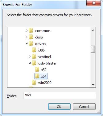
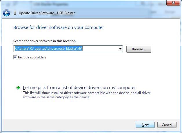
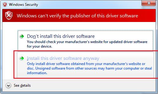
5 Browse to: C:\altera\71\quartus\drivers\usb-blaster\x64 After clicking Next, the following popup can appear: Answer Install this driver software anyway : DEPARTMENT OF ELECTRICAL AND COMPUTER ENGINEERING 5


6 If the installation is successful, you should receive: DEPARTMENT OF ELECTRICAL AND COMPUTER ENGINEERING 6


7 IMPLEMENTING SIMPLE PROJECT IN QUARTUS In this section, it is demonstrated how to put very simple circuit to the DE2 board. Inputs will be connected to switches, output will be connected to LED. DESIGN AN SIMULATING SCHEMATICS 1. Start Quartus II 7.1 Web Edition 2. Start new project wizard, enter the name of the project of: Click Next twice to go to the screen Family & Device Settings. Select the properties that are matching with your DE2 board. Take a look at the FPGA chip on the board to verify that below properties match with the ones you have: Family: Cyclone II Device: EP2C35F672C6 DEPARTMENT OF ELECTRICAL AND COMPUTER ENGINEERING 7


8 Click Finish. 3. Go to File -> New and select Block Diagram/Schematic File: 4. Add XOR gate to schematics: DEPARTMENT OF ELECTRICAL AND COMPUTER ENGINEERING 8
. 6.")
9 5. Use the same panel to add input and output pins, to get the following: Double click the pin to set its name (a, b for inputs, y for output). 6. Add simulation waveform file: go to File > New, choose Vector Waveform File: DEPARTMENT OF ELECTRICAL AND COMPUTER ENGINEERING 9
. 9.")
10 7. Save your files. Go to Assignments -> Settings, choose Simulator Settings section. Set: Simulation mode: Functional Simulation input: your saved vector waveform file. 8. Run Processing -> Start Compilation and Simulation. Wait for the message about the end of the processing (Compile and Simulation was successful). 9. Run Processing -> Start -> Start Analysis & Synthesis. DEPARTMENT OF ELECTRICAL AND COMPUTER ENGINEERING 10


11 10. Go to wector waveform view, right click the area on the left and select Insert -> Insert Node or Bus Click Node Finder: DEPARTMENT OF ELECTRICAL AND COMPUTER ENGINEERING 11

 or Forcing Low (0).")
12 Set Filter: Pins: all, click List, then click >> to add three nodes 11. Right clicking on the input waveform allows setting values. Use it to set test values for simulation, selecting either Forcing High (1) or Forcing Low (0). DEPARTMENT OF ELECTRICAL AND COMPUTER ENGINEERING 12

13 You should get: 12. Run Processing -> Generate Functional Simulation Netlist. 13. Start simulation: click Processing -> Start Simulation. You should get simulation results like below, confirming the operation of XOR gate: Now you are sure that your schematic works as expected, as the truth table for XOR function is verified: a b y Time ns ns 20ns ns 30ns ns 40ns The next step is to put your design to the board. DEPARTMENT OF ELECTRICAL AND COMPUTER ENGINEERING 13


14 PROGRAMMING DE2 BOARD 1. Assign pins. Go to Assignments -> Assignment Editor. 2. Set Category: Pin 3. Double click To field in row number Use the document Altera DE2 Board Pin Table between pin and physical element on the board. We want to use: Switch SW0 as first input a Switch SW1 as second input b Red LED 0 as the output. to determine the relation In the Altera DE2 Board Pin Table document, we can see, that switch SW0 is connected to pin PIN_N25: Thus we fill the following fields: Use the Altera DE2 Board Pin Table document to determine the location of two remaining elements: b, and y. You should get: Compile your project. DEPARTMENT OF ELECTRICAL AND COMPUTER ENGINEERING 14


15 5. Make sure, that SW19 RUN/PROG switch is in the RUN position. 6. Select Tools -> Programmer. Click Hardware Setup and select USB-Blaster from dropdown list. Close window. 7. Ensure that Mode value is set to JTAG. 8. If SOF file is not present on the list, click Add file to add it. Make sure Program/Configure checkbox is checked. 9. Click Start and wait for the board to be programmed. Observe System Messages to see if programming process ended with success. DEPARTMENT OF ELECTRICAL AND COMPUTER ENGINEERING 15

16 The board is now programmed. Two switches serve as a, b inputs to the gate, while the logic state of the output y is signaled by red LED. For more information, refer to Altera s DE2 Board starting guide DEPARTMENT OF ELECTRICAL AND COMPUTER ENGINEERING 16
17 CREATING A SYMBOL IN QUARTUS Quartus II software offers the possibility to create user defined elements. This simplifies the schematic design, as larger parts of the circuit can be represented as a block with inputs and outputs. Creating your own Full Adder block: 1. Create Full Adder circuit: 2. Compile your project 3. Create your element: go to File Create / Update Create Symbol Files for Current File. In the save dialog, put the name of new element, e.g. TestFA. After the process is done, the element can be selected from the list in Symbol Tool. Go to Windows Explorer and navigate to the folder that contains your project. You'll see TestFA.bsf file, that was created. This file contains the definition of your new symbol. DEPARTMENT OF ELECTRICAL AND COMPUTER ENGINEERING 17

18 When you type the name you gave to new element it will appear as any other element: Now it can be used in the schematic design. Double-clicking the element in the schematic, will show the inside design of your element. Using new element in another projects To use your element in another project, copy the file containing symbol definition (here: TestFA.bsf) and bdf file to the project directory. Then it will appear in the Symbol Tool. DEPARTMENT OF ELECTRICAL AND COMPUTER ENGINEERING 18
.")
19 PROGRAMMING DE2 BOARD WITH VERILOG IN QUARTUS DE2 offers four 50MHz signals. The frequency of 50MHz can be brought down using the following procedure. Create a new project named onehertz. Now, instead of creating a new Block Diagram/Schematic File, choose Verilog HDL File. Copy and paste the onehertz.v code (shown below). After compilation, the steps are the same as when using a schematic entry. Map the input clk_50mhz to PIN_N2, which is a 50MHz clock internal to the DE2 board. Map the output clk_1hz to LEDG8. On the DE2 board, you should see the LED on for 0.5 seconds (period of 1 second for both on and off part of the cycle). module onehertz(clk_50mhz, clk_1hz); input clk_50mhz; output clk_1hz; reg clk_1hz; reg [24:0] count; (posedge clk_50mhz) begin if(count == ) begin count <= 0; $dumpfile("f.vcd"); clk_1hz <= ~clk_1hz; end else begin count <= count + 1; end end endmodule DEPARTMENT OF ELECTRICAL AND COMPUTER ENGINEERING 19
20 TROUBLESHOOTING Quartus schematics: Compilation errors: o Make sure schematic does not contain any floating elements o Make sure that all input and output pins are connected to the elements No pins showing in node finder: o Make sure you have performed Compilation o Make sure you have performed Analysis & Synthesis Output signal changes with delay to input signals: o This is probably correct for Timing simulation. Probably you expect Functional simulation. Set that in Simulation Options. New symbol can t be found in other projects: o copy the file containing symbol definition (bsf file) and bdf file to the project directory. Then it will appear in the Symbol Tool. Programming the board: Quartus does not see the board: o Make sure that USB-Blaster is installed o Make sure that Windows device manager indicates that USB-Blaster device works properly o Make sure you connected USB cable to BLASTER port on the board Board is visible, but there are errors while programming the board: o Make sure that Family and Device values are set exactly to ones that you can read from FPGA chip on your board o Make sure that RUN/PROG switch is in RUN position LAB DELIVERIES: PRELAB: 1. Get familiar with Altera DE2 introduction documents Make yourself familiar with the following documents: Getting started with Altera DE2 Board: Altera DE2 Introduction Altera DE2 User Manual Altera: Quartus II Introduction Using Schematic Design 2. Prelab deliveries Write few paragraphs about FPGA technology DEPARTMENT OF ELECTRICAL AND COMPUTER ENGINEERING 20

21 LAB EXPERIMENTS: 1. Experiment 1: Configure DE2 board in Windows system Use the chapter Setting up DE2 board from this lab instruction to setup the DE2 board. Follow the section Implementing Simple Project In Quartus and implement the XOR gate on the DE2 board. Demonstrate working XOR to the TA. For more in depth features, and additional capabilities of Quartus see bit counter a) Create new project, draw the 4-bit counter given below. Connect A, B, C, and D to output pins that map to LEDR3, LEDR2, LEDR1, and LEDR0, respectively. Additionally, also connect A, B, C, and D to inputs of a 7447 decoder (which can be found in Quartus, see Figure below) There will be eight output pins for the 7447 decoder. To see how to map these pins to a seven segment display on the DE2 board see the Altera DE2 pin table or the DE2 User Manual (pages 30-31). Note that the 7447 is only meant to display one digit, i.e. the range 0-9 of the counter. EXTRA CREDIT: Use two 7-segment displays to display the decimal value of the counter for the entire 0-15 range using two digits. Use additional logic gates to implement this feature. DEPARTMENT OF ELECTRICAL AND COMPUTER ENGINEERING 21
22 3. Creating symbols 1. Create Full Adder as your own symbol. 2. Use option: File Create symbol to create Full Adder as your own symbol (see section Creating a Symbol in Quartus in the introductory part of this document) 3. Use your symbol to create ripple carry adder: 4. Programming DE2 board with Verilog 1. Implement the frequency divider using Verilog (see the section Programming DE2 Board with Verilog in Quartus in the introductory part of this document. 2. Analyze the Verilog code answer TA: what type of sequential circuit is implemented in there? 3. Replace the value of 24,999,999 so that the LED is on for 0.25 seconds (period of 0.5 seconds for both on and off cycle). Use the formula count = (50MHz * LED_time_on) 1 4. Reprogram the FPGA with your modification to verify. What is the meaning of this replaced value? Experiment with some other values and write down the conclusions. DEPARTMENT OF ELECTRICAL AND COMPUTER ENGINEERING 22
23 POSTLAB REPORT: Include the following elements in the report document: Section Element 1 Theory of operation Include a brief description of every element and phenomenon that appears during the experiments. 2 Prelab report Results of the experiments Experiment Experiment Results a. Screenshot of pin assignments 1 b. Picture of DE2 during operation a. Screenshot of pin assignments 2 b. Screenshot of schematic in Quartus 3 c. Picture of DE2 during operation a. Truth table 3 b. Screenshot of the FA schematic c. Screenshot of the Ripple Carry circuit a. screenshot of pin assignments 4 b. screenshot of your Verilog file with your modified count value Answer the questions Question no. Question 1 What is pin assignment in DE2? 4 When connecting LEDs in DE2 board, why resistors are not used in 2 schematic? What is the technical meaning of the value that controls the frequency division 3 in experiment 4? 5 Conclusions Write down your conclusions, things learned, problems met during the lab and how they were solved, etc. 6 Attachments Zip your projects. Send through WebCampus as zip, or provide link to the zip file to shared location List of attachments to deliver: 1. Your symbol files for FA 2. Project of Ripple Carry Adder 3. Project of counter 4. Project with Verilog code References: 1. DE2 pin table: 2. Altera DE2 Introduction 3. Getting started with Altera DE2 Board: 4. Altera: Quartus II Introduction Using Schematic Design 5. Altera DE2 User Manual 6. Datasheets of 7400 series chips: 7. Using DE2 oscillator: DEPARTMENT OF ELECTRICAL AND COMPUTER ENGINEERING 23
EMT1250 LABORATORY EXPERIMENT. EXPERIMENT # 7: VHDL and DE2 Board. Name: Date:
 EXPERIMENT # 7: VHDL and DE2 Board Name: Date: Equipment/Parts Needed: Quartus II R Web Edition V9.1 SP2 software by Altera Corporation USB drive to save your files Objective: Learn how to create and modify
Terasic DE0 Field Programmable Gate Array (FPGA) Development Board
 Development Board") Lecture FPGA-01 DE0 FPGA Development Board and Quartus II 9.1 FPGA Design Software Terasic DE0 Field Programmable Gate Array (FPGA) Development Board 1 May 16, 2013 3 Layout and Components of DE0 May 16,
Lecture FPGA-01 DE0 FPGA Development Board and Quartus II 9.1 FPGA Design Software Terasic DE0 Field Programmable Gate Array (FPGA) Development Board 1 May 16, 2013 3 Layout and Components of DE0 May 16,
PRELAB! Read the entire lab, and complete the prelab questions (Q1- Q3) on the answer sheet before coming to the laboratory.
 on the answer sheet before coming to the laboratory.") PRELAB! Read the entire lab, and complete the prelab questions (Q1- Q3) on the answer sheet before coming to the laboratory. 1.0 Objectives In this lab you will get familiar with the concept of using the
PRELAB! Read the entire lab, and complete the prelab questions (Q1- Q3) on the answer sheet before coming to the laboratory. 1.0 Objectives In this lab you will get familiar with the concept of using the
Lab 2 EECE473 Computer Organization & Architecture University of Maine
 Lab 2: Verilog Programming Instructor: Yifeng Zhu 50 Points Objectives: 1. Quatus II Programming assignment: PIN assignments, LEDs, switches; 2. Download and test the design on Altera DE2 board 3. Create
Introduction to VHDL Design on Quartus II and DE2 Board
 ECP3116 Digital Computer Design Lab Experiment Duration: 3 hours Introduction to VHDL Design on Quartus II and DE2 Board Objective To learn how to create projects using Quartus II, design circuits and
FPGA Introductory Tutorial: Part 1
 FPGA Introductory Tutorial: Part 1 This tutorial is designed to assist in learning the basics of the Altera Quartus II v9.0 software. Part 1 of the tutorial will cover the basics of creating a Project,
Tutorial on Quartus II Introduction Using Verilog Code
 Tutorial on Quartus II Introduction Using Verilog Code (Version 15) 1 Introduction This tutorial presents an introduction to the Quartus II CAD system. It gives a general overview of a typical CAD flow
QUARTUS II Altera Corporation
 QUARTUS II Quartus II Design Flow Design Entry Timing Constraints Synthesis Placement and Routing Timing, Area, Power Optimization Timing and Power Analyzer Optimized Design 2 Can I still use a Processor?
NIOS CPU Based Embedded Computer System on Programmable Chip
 1 Objectives NIOS CPU Based Embedded Computer System on Programmable Chip EE8205: Embedded Computer Systems This lab has been constructed to introduce the development of dedicated embedded system based
EMT1250 LABORATORY EXPERIMENT. EXPERIMENT # 10: Implementing Binary Adders. Name: Date:
 EXPERIMENT # 10: Implementing Binary Adders Name: Date: Equipment/Parts Needed: PC (Altera Quartus II V9.1 installed) DE-2 board Objective: Design a half adder by extracting the Boolean equation from a
Chapter 2 Getting Hands on Altera Quartus II Software
 Chapter 2 Getting Hands on Altera Quartus II Software Contents 2.1 Installation of Software... 20 2.2 Setting Up of License... 21 2.3 Creation of First Embedded System Project... 22 2.4 Project Building
Laboratory Exercise 8
 Laboratory Exercise 8 Memory Blocks In computer systems it is necessary to provide a substantial amount of memory. If a system is implemented using FPGA technology it is possible to provide some amount
Tutorial on Quartus II Introduction Using Schematic Designs
 Tutorial on Quartus II Introduction Using Schematic Designs (Version 15) 1 Introduction This tutorial presents an introduction to the Quartus II CAD system. It gives a general overview of a typical CAD
ECE 3610 Microprocessing Systems Lab #1 Verilog Design of the TOC Using Quartus II
 ECE 3610 Microprocessing Systems Lab #1 Verilog Design of the TOC Using Quartus II This lab manual presents an introduction to the Quartus II Computer Aided Design (CAD) system. This manual gives step-by-step
ECSE-323 Digital System Design. Lab #1 Using the Altera Quartus II Software Fall 2008
 1 ECSE-323 Digital System Design Lab #1 Using the Altera Quartus II Software Fall 2008 2 Introduction. In this lab you will learn the basics of the Altera Quartus II FPGA design software through following
Laboratory 4 Design a Muti-bit Counter
 Laboratory 4 Design a Muti-bit Counter Background A. Approach I: Design 3-bit counter with and clear T-type flip-flop is shown in Figure 1. A T flip-flop is obtained from a JK flip-flop by tying the J
Quartus II Introduction Using Verilog Design
 Quartus II Introduction Using Verilog Design This tutorial presents an introduction to the Quartus R II CAD system. It gives a general overview of a typical CAD flow for designing circuits that are implemented
NIOS CPU Based Embedded Computer System on Programmable Chip
 NIOS CPU Based Embedded Computer System on Programmable Chip 1 Lab Objectives EE8205: Embedded Computer Systems NIOS-II SoPC: PART-I This lab has been constructed to introduce the development of dedicated
Laboratory 4 Design a Muti-bit Counter and Programming a FPGA
 Laboratory 4 Design a Muti-bit Counter and Programming a FPGA For your report: The problem written in English The flowchart or function table to solve the problem if it is necessary The design entry included
Lab 6: Integrated the Decoder with Muti-bit Counter and Programming a FPGA
 Lab 6: Integrated the Decoder with Muti-bit Counter and Programming a FPGA For your report: The problem written in English The flowchart or function table to solve the problem if it is necessary The design
EE 231 Fall EE 231 Lab 2
 EE 231 Lab 2 Introduction to Verilog HDL and Quartus In the previous lab you designed simple circuits using discrete chips. In this lab you will do the same but by programming the CPLD. At the end of the
Quartus II Introduction Using Schematic Design
 Quartus II Introduction Using Schematic Design This tutorial presents an introduction to the Quartus R II CAD system. It gives a general overview of a typical CAD flow for designing circuits that are implemented
NOTE: This tutorial contains many large illustrations. Page breaks have been added to keep images on the same page as the step that they represent.
 CSE 352 Tutorial # 4 Synthesizing onto an FPGA Objectives This tutorial will walk you through the steps of implementing a design made in Active-HDL onto the Altera Cyclone II FPGA NOTE: This tutorial contains
University of California, Davis Department of Electrical and Computer Engineering. Lab 1: Implementing Combinational Logic in the MAX10 FPGA
 1 University of California, Davis Department of Electrical and Computer Engineering EEC180B DIGITAL SYSTEMS II Winter Quarter 2018 Lab 1: Implementing Combinational Logic in the MAX10 FPGA Objective: This
Laboratory Exercise 7
 Laboratory Exercise 7 Finite State Machines This is an exercise in using finite state machines. Part I We wish to implement a finite state machine (FSM) that recognizes two specific sequences of applied
Quick Tutorial for Quartus II & ModelSim Altera
 Quick Tutorial for Quartus II & ModelSim Altera By Ziqiang Patrick Huang Hudson 213c Ziqiang.huang@duke.edu Download & Installation For Windows or Linux users : Download Quartus II Web Edition v13.0 (ModelSim
EE 231 Fall Lab 1: Introduction to Verilog HDL and Altera IDE
 Lab 1: Introduction to Verilog HDL and Altera IDE Introduction In this lab you will design simple circuits by programming the Field-Programmable Gate Array (FPGA). At the end of the lab you should be able
SOPC LAB1. I. Introduction. II. Lab contents. 4-bit count up counter. Advanced VLSI Due Wednesday, 01/08/2003
 SOPC LAB1 I. Introduction The purpose of this lab is to familiarize you with all the items in the kit. This tutorial tells you how to develop FPGA system in Quartus II. You are ready to begin using the
ENEE245 Digital Circuits and Systems Lab Manual
 ENEE245 Digital Circuits and Systems Lab Manual Department of Engineering, Physical & Computer Sciences Montgomery College Version 1.1 Copyright Prof. Lan Xiang (Do not distribute without permission) 1
Quartus II Introduction Using Verilog Designs. 1 Introduction. For Quartus II 12.0
 Quartus II Introduction Using Verilog Designs For Quartus II 12.0 1 Introduction This tutorial presents an introduction to the Quartus II CAD system. It gives a general overview of a typical CAD flow for
Laboratory Exercise 1
 Laboratory Exercise 1 Switches, Lights, and Multiplexers The purpose of this exercise is to learn how to connect simple input and output devices to an FPGA chip and implement a circuit that uses these
Chapter 2: Hardware Design Flow Using Verilog in Quartus II
 Chapter 2: Hardware Design Flow Using Verilog in Quartus II 2.1 Introduction to Quartus II System Development Software This chapter is an introduction to the Quartus II software that will be used for analysis
IMPLEMENTING COUNTERS
 EECS:6660:0xxField Programmable Gate Arrays s11l1_fpga.fm - 1 Lab Assignment #1 Due Thursday, March 31 2011 IMPLEMENTING COUNTERS 1. OBJECTIVES - learning the VHDL implementation process using Language
SignalTap II with Verilog Designs. 1 Introduction. For Quartus II 13.1
 SignalTap II with Verilog Designs For Quartus II 13.1 1 Introduction This tutorial explains how to use the SignalTap II feature within Altera s Quartus II software. The SignalTap II Embedded Logic Analyzer
Physics 536 Spring Illustrating the FPGA design process using Quartus II design software and the Cyclone II FPGA Starter Board.
 Physics 536 Spring 2009 Illustrating the FPGA design process using Quartus II design software and the Cyclone II FPGA Starter Board. Digital logic: Equivalent to a large number of discrete logic elements
University of Massachusetts Amherst Computer Systems Lab 2 (ECE 354) Spring Lab 1: Using Nios 2 processor for code execution on FPGA
 Spring Lab 1: Using Nios 2 processor for code execution on FPGA") University of Massachusetts Amherst Computer Systems Lab 2 (ECE 354) Spring 2007 Lab 1: Using Nios 2 processor for code execution on FPGA Objectives: After the completion of this lab: 1. You will understand
University of Massachusetts Amherst Computer Systems Lab 2 (ECE 354) Spring 2007 Lab 1: Using Nios 2 processor for code execution on FPGA Objectives: After the completion of this lab: 1. You will understand
EMT1250 LABORATORY EXPERIMENT. EXPERIMENT # 6: Quartus II Tutorial and Practice. Name: Date:
 EXPERIMENT # 6: Quartus II Tutorial and Practice Name: Date: Equipment/Parts Needed: Quartus II R Web Edition V9.1 SP2 software by Altera Corporation USB drive to save your files Objective: Learn how to
SFWR ENG 2DA4 Lab 1. Announcements: Marking Scheme: Lab Safety Manual:
 SFWR ENG 2DA4 Lab 1 First lab Week of: Sept. 17, 2018 Prep Due week of: (8:40/14:40), Sept. 24, 2018 Demo Due Week of: (11:20/17:20), Sept. 24, 2018 Assignment due in class: 13:40, Sept. 28, 2018 Announcements:
DE2 Board & Quartus II Software
 January 23, 2015 Contact and Office Hours Teaching Assistant (TA) Sergio Contreras Office Office Hours Email SEB 3259 Tuesday & Thursday 12:30-2:00 PM Wednesday 1:30-3:30 PM contre47@nevada.unlv.edu Syllabus
Lab 2: Introduction to Verilog HDL and Quartus
 Lab 2: Introduction to Verilog HDL and Quartus September 16, 2008 In the previous lab you designed simple circuits using discrete chips. In this lab you will do the same but by programming the CPLD. At
ENEE245 Digital Circuits and Systems Lab Manual
 ENEE245 Digital Circuits and Systems Lab Manual Department of Engineering, Physical & Computer Sciences Montgomery College Modified Fall 2017 Copyright Prof. Lan Xiang (Do not distribute without permission)
NIOS CPU Based Embedded Computer System on Programmable Chip
 NIOS CPU Based Embedded Computer System on Programmable Chip EE8205: Embedded Computer Systems NIOS-II SoPC: PART-II 1 Introduction This lab has been constructed to introduce the development of dedicated
Introduction to the Altera SOPC Builder Using Verilog Design
 Introduction to the Altera SOPC Builder Using Verilog Design This tutorial presents an introduction to Altera s SOPC Builder software, which is used to implement a system that uses the Nios II processor
CET4805 Component and Subsystem Design II. EXPERIMENT # 5: Adders. Name: Date:
 EXPERIMENT # 5: Adders Name: Date: Equipment/Parts Needed: Quartus II R Web Edition V9.1 SP2 software by Altera Corporation USB drive to save your files Objective: Design a half adder by extracting the
Engineering 303 Digital Logic Design Spring 2017
 Engineering 303 Digital Logic Design Spring 2017 LAB 1 Introduction to Combo Logic and Quartus Deliverables: 0) A Simple Verilog Combinatorial Circuit 1) A Simple Block Diagram Combinatorial Circuit 2)
University of Florida EEL 3701 Dr. Eric M. Schwartz Department of Electrical & Computer Engineering Revision 0 12-Jun-16
 Page 1/14 Quartus Tutorial with Basic Graphical Gate Entry and Simulation Example Problem Given the logic equation Y = A*/B + /C, implement this equation using a two input AND gate, a two input OR gate
CHAPTER 1 INTRODUCTION... 1 CHAPTER 2 ASSIGN THE DEVICE... 7 CHAPTER 3 DESIGN ENTRY CHAPTER 4 COMPILE AND VERIFY YOUR DESIGN...
 CONTENTS CHAPTER 1 INTRODUCTION... 1 1.1 DESIGN FLOW... 1 1.2 BEFORE YOU BEGIN... 2 1.3 WHAT YOU WILL LEARN... 6 CHAPTER 2 ASSIGN THE DEVICE... 7 2.1 ASSIGN THE DEVICE... 7 CHAPTER 3 DESIGN ENTRY... 11
UNIVERSITI MALAYSIA PERLIS
 UNIVERSITI MALAYSIA PERLIS SCHOOL OF COMPUTER & COMMUNICATIONS ENGINEERING EKT 124 LABORATORY MODULE INTRODUCTION TO QUARTUS II DESIGN SOFTWARE : INTRODUCTION TO QUARTUS II DESIGN SOFTWARE OBJECTIVES To
Tutorial for Altera DE1 and Quartus II
 Tutorial for Altera DE1 and Quartus II Qin-Zhong Ye December, 2013 This tutorial teaches you the basic steps to use Quartus II version 13.0 to program Altera s FPGA, Cyclone II EP2C20 on the Development
EXPERIMENT 1. INTRODUCTION TO ALTERA
 EXPERIMENT 1. INTRODUCTION TO ALTERA I. Introduction I.I Objectives In this experiment, you will learn computer aided digital design and verification of it using Field Programmable Gate Arrays (FPGA).
2 nd Year Laboratory. Experiment: FPGA Design with Verilog. Department of Electrical & Electronic Engineering. Imperial College London.
 Department of Electrical & Electronic Engineering 2 nd Year Laboratory Experiment: FPGA Design with Verilog Objectives By the end of this experiment, you should know: How to design digital circuits using
E85: Digital Design and Computer Engineering Lab 2: FPGA Tools and Combinatorial Logic Design
 E85: Digital Design and Computer Engineering Lab 2: FPGA Tools and Combinatorial Logic Design Objective The purpose of this lab is to learn to use Field Programmable Gate Array (FPGA) tools to simulate
DKAN0011A Setting Up a Nios II System with SDRAM on the DE2
 DKAN0011A Setting Up a Nios II System with SDRAM on the DE2 04 November 2009 Introduction This tutorial details how to set up and instantiate a Nios II system on Terasic Technologies, Inc. s DE2 Altera
Introduction to the Altera SOPC Builder Using Verilog Designs. 1 Introduction
 Introduction to the Altera SOPC Builder Using Verilog Designs 1 Introduction This tutorial presents an introduction to Altera s SOPC Builder software, which is used to implement a system that uses the
Laboratory Exercise 3 Comparative Analysis of Hardware and Emulation Forms of Signed 32-Bit Multiplication
 Laboratory Exercise 3 Comparative Analysis of Hardware and Emulation Forms of Signed 32-Bit Multiplication Introduction All processors offer some form of instructions to add, subtract, and manipulate data.
SCHEMATIC DESIGN IN QUARTUS
 SCHEMATIC DESIGN IN QUARTUS Consider the design of a three-bit prime number detector. Figure 1 shows the block diagram and truth table. The inputs are binary signals A, B, and C while the output is binary
Chip Design with FPGA Design Tools
 Chip Design with FPGA Design Tools Intern: Supervisor: Antoine Vazquez Janusz Zalewski Florida Gulf Coast University Fort Myers, FL 33928 V1.9, August 28 th. Page 1 1. Introduction FPGA is abbreviation
DOWNLOADING DESIGNS TO THE ALTERA DE10-LITE FPGA
 DOWNLOADING DESIGNS TO THE ALTERA DE10-LITE FPGA Consider the design of a three-bit prime number detector completed in the MSOE schematic entry tutorial. Figure 1 shows the block diagram and truth table.
Digital Systems Laboratory
 2012 Fall CSE140L Digital Systems Laboratory by Dr. Choon Kim CSE Department UCSD 1 Welcome to CSE140L! 2 3-way Light Controller, 2-1 MUX, Majority Detector, 7- seg Display, Binary-to- Decimal converter.
CSCB58 - Lab 0. Intro to The Lab & The DE2 Board. Prelab /4 Part I (in-lab) /1 Part II (in-lab) /1
 /1 Part II (in-lab) /1") CSCB58 - Lab 0 Intro to The Lab & The DE2 Board Learning Objectives This week we will be getting you familiar with the lab and the boards that we will be using in later labs. You will also learn how to
CSCB58 - Lab 0 Intro to The Lab & The DE2 Board Learning Objectives This week we will be getting you familiar with the lab and the boards that we will be using in later labs. You will also learn how to
1 Introduction 2. 2 Background 3. 3 Getting Started 4. 4 Starting a New Project 6. 5 Design Entry Using VHDL Code 13
 Quartus Prime Introduction Using VHDL Designs For Quartus Prime 17.0 Contents 1 Introduction 2 2 Background 3 3 Getting Started 4 3.1 Quartus Prime Online Help................................................................................................
University of Massachusetts Amherst Computer Systems Lab 1 (ECE 354) LAB 1 Reference Manual
 LAB 1 Reference Manual") University of Massachusetts Amherst Computer Systems Lab 1 (ECE 354) LAB 1 Reference Manual Lab 1: Using NIOS II processor for code execution on FPGA Objectives: 1. Understand the typical design flow in
University of Massachusetts Amherst Computer Systems Lab 1 (ECE 354) LAB 1 Reference Manual Lab 1: Using NIOS II processor for code execution on FPGA Objectives: 1. Understand the typical design flow in
CSEE W4840 Embedded System Design Lab 1
 CSEE W4840 Embedded System Design Lab 1 Stephen A. Edwards Due January 31, 2008 Abstract Learn to use the Altera Quartus development envrionment and the DE2 boards by implementing a small hardware design
FPGA Development Board Hardware and I/O Features
 CHAPTER 2 FPGA Development Board Hardware and I/O Features Photo: The Altera DE1 board contains a Cyclone II FPGA, external SRAM, SDRAM & Flash memory, and a wide assortment of I/O devices and connectors.
Advanced Electronics Lab.
 College of Engineering Course Book of 2010-2011 Advanced Electronics Lab. Mr. Araz Sabir Ameen M.Sc. in Electronics & Communications ALTERA DE2 Development and Education Board DE2 Package: The DE2 package
Contents. Appendix B HDL Entry Tutorial 2 Page 1 of 14
 Appendix B HDL Entry Tutorial 2 Page 1 of 14 Contents Appendix B HDL Entry Tutorial 2...2 B.1 Getting Started...2 B.1.1 Preparing a Folder for the Project...2 B.1.2 Starting Quartus II...2 B.1.3 Creating
INTRODUCTION TO DE2 SYSTEM INTERFACES
 EECS:6660:0xxField Programmable Gate Arrays s08l5a.fm - 1 Lab Assignment #5 INTRODUCTION TO DE2 SYSTEM INTERFACES 1. OBJECTIVES - Becoming familiar with the system interface to seven segment LED displays
University of Florida EEL 3701 Dr. Eric M. Schwartz Madison Emas, TA Department of Electrical & Computer Engineering Revision 1 5-Jun-17
 Page 1/14 Example Problem Given the logic equation Y = A*/B + /C, implement this equation using a two input AND gate, a two input OR gate and two inverters under the Quartus environment. Upon completion
The development board used in this class is ALTERA s DE The board provides the following hardware:
 Lab 1 The goal of this lab is to get familiar with the mechanics of designing digital systems using VHDL and ALTERA s FPGAs. The development board used in this class is ALTERA s DE2-115. The board provides
CSE P567 - Winter 2010 Lab 1 Introduction to FGPA CAD Tools
 CSE P567 - Winter 2010 Lab 1 Introduction to FGPA CAD Tools This is a tutorial introduction to the process of designing circuits using a set of modern design tools. While the tools we will be using (Altera
Tutorial 2 Implementing Circuits in Altera Devices
 Appendix C Tutorial 2 Implementing Circuits in Altera Devices In this tutorial we describe how to use the physical design tools in Quartus II. In addition to the modules used in Tutorial 1, the following
structure syntax different levels of abstraction
 This and the next lectures are about Verilog HDL, which, together with another language VHDL, are the most popular hardware languages used in industry. Verilog is only a tool; this course is about digital
Here is a list of lecture objectives. They are provided for you to reflect on what you are supposed to learn, rather than an introduction to this
 This and the next lectures are about Verilog HDL, which, together with another language VHDL, are the most popular hardware languages used in industry. Verilog is only a tool; this course is about digital
UNIVERSITY OF CALIFORNIA, DAVIS Department of Electrical and Computer Engineering. EEC180A DIGITAL SYSTEMS I Winter 2015
 UNIVERSITY OF CALIFORNIA, DAVIS Department of Electrical and Computer Engineering EEC180A DIGITAL SYSTEMS I Winter 2015 LAB 1: Introduction to Quartus II Schematic Capture and ModelSim Simulation This
Altera DE1 Board DE1. Development and Education Board. User Manual. Copyright 2006 Altera Corporation
 Altera DE1 Board DE1 Development and Education Board User Manual Version 1.1 Copyright 2006 Altera Corporation Chapter 2 Altera DE1 Board This chapter presents the features and design characteristics of
ECE241 - Digital Systems. University of Toronto. Lab #2 - Fall Introduction Computer-Aided Design Software, the DE2 Board and Simple Logic
 ECE24 - Digital Sstems Universit of Toronto Lab #2 - Fall 28 Introduction Computer-Aided Design Software, the DE2 Board and Simple Logic. Introduction The purpose of this eercise is to introduce ou to
EARTH PEOPLE TECHNOLOGY. ODIN-LINK BLE + MAXPROLOGIC Development System User Manual
 EARTH PEOPLE TECHNOLOGY ODIN-LINK BLE + MAXPROLOGIC Development System User Manual This User Manual covers the Odin-Link and MaxProLogic Development System. The Odin-Link board includes the Texas Instruments
AN 818: Static Update Partial Reconfiguration Tutorial
 AN 818: Static Update Partial Reconfiguration Tutorial for Intel Stratix 10 GX Updated for Intel Quartus Prime Design Suite: 18.1 Subscribe Latest document on the web: PDF HTML Contents Contents 1. Static
Experiment VERI: FPGA Design with Verilog (Part 1)
") Experiment VERI: Department of Electrical & Electronic Engineering 2nd Year Laboratory Experiment VERI: FPGA Design with Verilog (Part 1) (webpage: www.ee.ic.ac.uk/pcheung/teaching/e2_experiment /) Objectives
Experiment VERI: Department of Electrical & Electronic Engineering 2nd Year Laboratory Experiment VERI: FPGA Design with Verilog (Part 1) (webpage: www.ee.ic.ac.uk/pcheung/teaching/e2_experiment /) Objectives
Name EGR 2131 Lab #6 Number Representation and Arithmetic Circuits
 Name EGR 2131 Lab #6 Number Representation and Arithmetic Circuits Equipment and Components Quartus software and Altera DE2-115 board PART 1: Number Representation in Microsoft Calculator. First, let s
Standard Logic Chips and National Instruments ELVIS Breadboarding for Combinational Logic Circuits
 ECE380 Digital Logic: Design Activity #4 Standard Logic Chips and National Instruments ELVIS Breadboarding for Combinational Logic Circuits INTRODUCTION In Design Activity #4 you will use the National
CHAPTER 1 Introduction of the tnano Board CHAPTER 2 tnano Board Architecture CHAPTER 3 Using the tnano Board... 8
 CONTENTS CHAPTER 1 Introduction of the tnano Board... 2 1.1 Features...2 1.2 About the KIT...4 1.3 Getting Help...4 CHAPTER 2 tnano Board Architecture... 5 2.1 Layout and Components...5 2.2 Block Diagram
E85: Digital Design and Computer Architecture J. Spjut and R. Wang Spring 2014
 E85: Digital Design and Computer Architecture J. Spjut and R. Wang Spring 2014 Lab 1: Full Adder Introduction In this lab you will design a simple digital circuit called a full adder. Along the way, you
CSCB58 - Lab 3. Prelab /3 Part I (in-lab) /2 Part II (in-lab) /2 TOTAL /8
 /2 Part II (in-lab) /2 TOTAL /8") CSCB58 - Lab 3 Latches, Flip-flops, and Registers Learning Objectives The purpose of this exercise is to investigate the fundamental synchronous logic elements: latches, flip-flops, and registers. Prelab
CSCB58 - Lab 3 Latches, Flip-flops, and Registers Learning Objectives The purpose of this exercise is to investigate the fundamental synchronous logic elements: latches, flip-flops, and registers. Prelab
Lab 3: Standard Combinational Components
 Lab 3: Standard Combinational Components Purpose In this lab you will implement several combinational circuits on the DE1 development board to test and verify their operations. Introduction Using a high-level
Altera Quartus II Tutorial ECE 552
 Altera Quartus II Tutorial ECE 552 Quartus II by Altera is a PLD Design Software which is suitable for high-density Field-Programmable Gate Array (FPGA) designs, low-cost FPGA designs, and Complex Programmable
CPEN 230L: Introduction to Digital Logic Laboratory Lab #6: Verilog and ModelSim
 CPEN 230L: Introduction to Digital Logic Laboratory Lab #6: Verilog and ModelSim Purpose Define logic expressions in Verilog using register transfer level (RTL) and structural models. Use Quartus II to
The University of Toledo EECS:6660:0xxField Programmable Gate Arrays s09l1.fm - 1 Dr. A.D. Johnson
 EECS:6660:0xxField Programmable Gate Arrays s09l1.fm - 1 Lab Assignment #1 Due: Friday, February 27 2009 Introduction to Altera Quartus II Environment using VHDL Entry 1. Objectives - introduction to Quartus
Laboratory Exercise 9
 Laboratory Exercise 9 Figure 1 shows a digital system that contains a number of -bit registers, a multiplexer, an adder/subtracter unit, a counter, and a control unit. Data is input to this system via
DE2 Function Library Manual
 ALTERA DE2 Function Library Version 1.0 A L T E R A D E 2 D E V E L O P M E N T B O A R D DE2 Function Library Manual Celoxica, the Celoxica logo and Handel-C are trademarks of Celoxica Limited. Altera,
CSEE W4840 Embedded System Design Lab 1
 CSEE W4840 Embedded System Design Lab 1 Stephen A. Edwards Due February 2, 2009 Abstract Learn to use the Altera Quartus development envrionment and the DE2 boards by implementing a small hardware design
COSC 3215 Embedded Systems Laboratory
 COSC 3215 Embedded Systems Laboratory Lab 5 The Altera, Verilog and QuartusII Introduction This lab is an introduction to the Altera FPGA development board and the accompanying FPGA programming environment
EXPERIMENT NUMBER 7 HIERARCHICAL DESIGN OF A FOUR BIT ADDER (EDA-2)
") 7-1 EXPERIMENT NUMBER 7 HIERARCHICAL DESIGN OF A FOUR BIT ADDER (EDA-2) Purpose The purpose of this exercise is to explore more advanced features of schematic based design. In particular you will go through
7-1 EXPERIMENT NUMBER 7 HIERARCHICAL DESIGN OF A FOUR BIT ADDER (EDA-2) Purpose The purpose of this exercise is to explore more advanced features of schematic based design. In particular you will go through
CSEE W4840 Embedded System Design Lab 1
 CSEE W4840 Embedded System Design Lab 1 Stephen A. Edwards Due February 3, 2011 Abstract Learn to use the Altera Quartus development envrionment and the DE2 boards by implementing a small hardware design
My First FPGA for Altera DE2-115 Board
 My First FPGA for Altera DE2-115 Board 數位電路實驗 TA: 吳柏辰 Author: Trumen Outline Complete Your Verilog Design Assign The Device Add a PLL Megafunction Assign the Pins Create a Default TimeQuest SDC File Compile
PREFACE. Changes to the SOPC Edition
 PREFACE Changes to the SOPC Edition Rapid Prototyping of Digital Systems provides an exciting and challenging laboratory component for undergraduate digital logic and computer design courses using FPGAs
Lab 4: Register File and Memory 50 points Instructor: Yifeng Zhu Due: One week
 Objectives: Lab 4: Register File and Memory 50 points Instructor: Yifeng Zhu Due: One week Build Register File Build Instruction Memory and Data Memory 1. Overview A combinational circuit neither contains
AN 825: Partially Reconfiguring a Design on Intel Stratix 10 GX FPGA Development Board
 AN 825: Partially Reconfiguring a Design on Intel Stratix 10 GX FPGA Updated for Intel Quartus Prime Design Suite: 18.1 Subscribe Latest document on the web: PDF HTML Contents Contents Partially Reconfiguring
EN2911X: Reconfigurable Computing Lecture 01: Introduction
 EN2911X: Reconfigurable Computing Lecture 01: Introduction Prof. Sherief Reda Division of Engineering, Brown University Fall 2009 Methods for executing computations Hardware (Application Specific Integrated