Introduction to NI Multisim & Ultiboard
|
|
|
- Sydney Hall
- 6 years ago
- Views:
Transcription
1 George Washington University School of Engineering and Applied Science Electrical and Computer Engineering Department Introduction to NI Multisim & Ultiboard Dr. Amir Aslani 8/20/2017
2 2
3 Outline Design & Simulate a Low Pass Filter in Multisim Create a Netlist PCB design in Ultiboard Create new parts and new footprints Generate Gerber Files 3
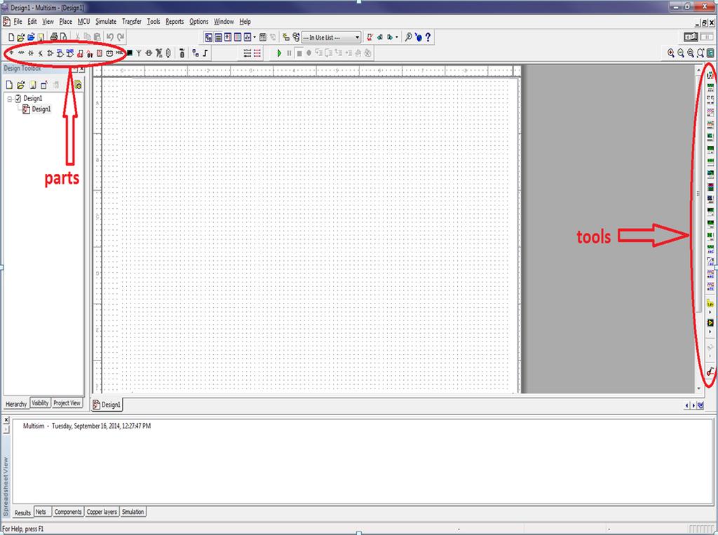
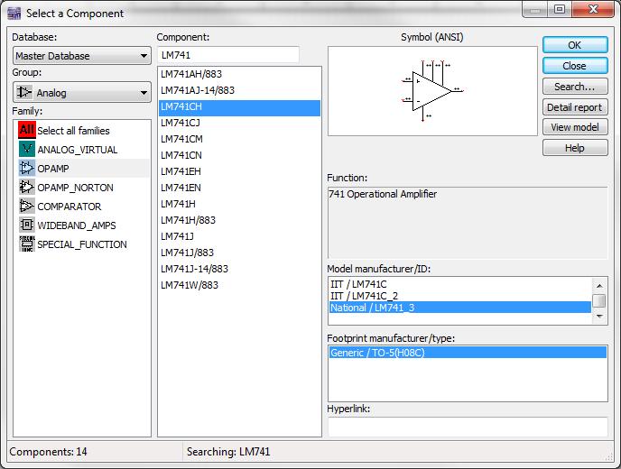
4 Placing components in Multisim 1. Select Place >> Component. 2. In the Select a Component dialog box, set the interface to the following settings. You have now selected the Analog group, and the OPAMP family. 3. In the Component Field select LM741CH or LM741AH/ Click on OK. 5. Place the OPAMP in your schematic area with a leftclick of the mouse. 6. Right click and select Flip vertical 4
5 5
6 Placing Resistors Select Place >> Component. In the Select a Component dialog box, set the dialog to the following settings circled in red. You have now selected the Basic group and the Resistor family In the "Component Field" type the value of the resistor in this case 2K. Make sure to pick a resistor that has the right footprint Click on OK, to place the part. Place the resistor in your schematic area with a left-click of the mouse. You still return to the Component Selection guide. Pick one more resistor by selecting the Basic group and the Resistor family. In the Component Field type the value of the resistor in this case 1K. Click on OK, to place the part. Place the resistor in your schematic area with a left-click of the mouse. 6
7 Placing Capacitors Select Place >> Component. In the Select a Component dialog box, select the Basic group and the Capacitor family. In the "Component Field" type the value of the capacitor in this case 0.08uF. Make sure to pick a capacitor that has the right footprint 7
8 Your design should look like this 8
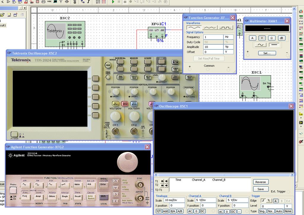
9 To place the Source Go to the right most side of your screen Hover mouse over each icon to find Function Generator Place source. Double click on it. Change Amplitude to 1 Vp and Frequency to 10 Hz. Right click on source and select Flip horizontal Connect the ground (center lead) to GROUND Connect the positive lead (+) to R2 Alternatively, instead of Function Generator we can use an AC Voltage Source (Place Component Sources Signal Voltage Source AC_Voltage) 9
10 Your design should look like this 10
11 Finished Wiring (just click the leads) 11
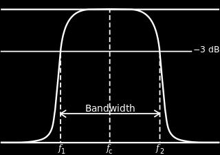
12 Adding Rails (DC Power Supply) Place >> Component Group Sources Family SIGNAL_VOLTAGE_SOURCE Component - VCC Place two of these. Rename one VEE and set to -5v The other should remain VCC at 5v, flip this one vertically Connect VCC to lead 7, VEE to lead 4 12
13 If it does not look like this, switch to PolySci. 13
14 As we said we could have used an AC voltage source as well: 14
15 Setting up an Analysis & Simulation: 1. Select Simulate >> Instruments >> Measurement Probe 2. Place the probe with a left-click of the mouse at the output of your circuit. The node is now called Probe To change its name double-click on the yellow field, and in the RefDes section, rename the probe from Probe 1 to Vout. 15

16 Your design should look like this 16
 3.")
17 Running AC Analysis 1. Under Simulate Analysis AC analysis 2. In the AC Analysis dialog box: Set start frequency to 1 Hz Set stop frequency to 100 KHz Set the Vertical Scale to Decibel this generates Bode plots (magnitude and phase responses) 3. Select the Output tab 4. In the Variables in Circuit section, select V(Vout) parameter 5. Click on the Add button 6. Click on the Simulate button. You will now see your simulation data 17
18 18

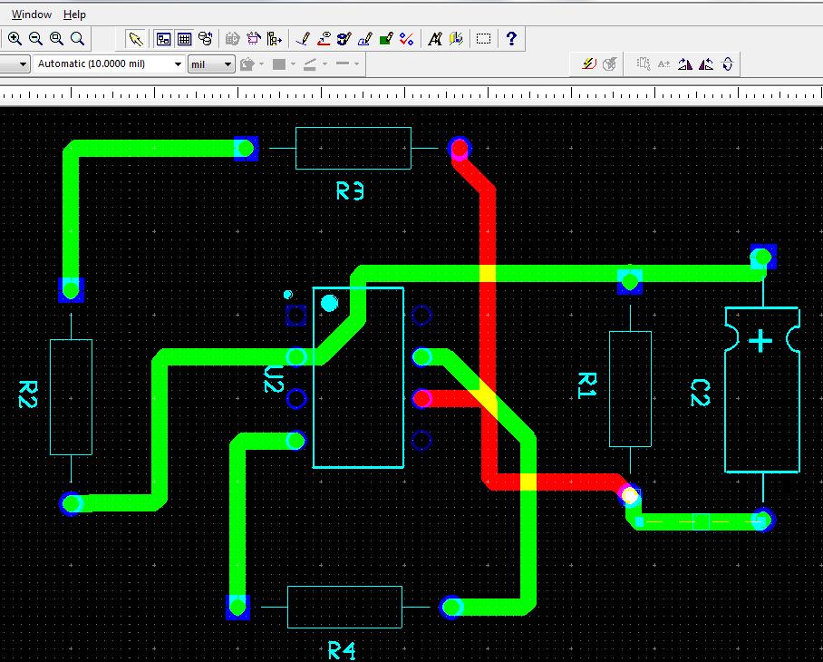
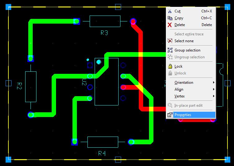
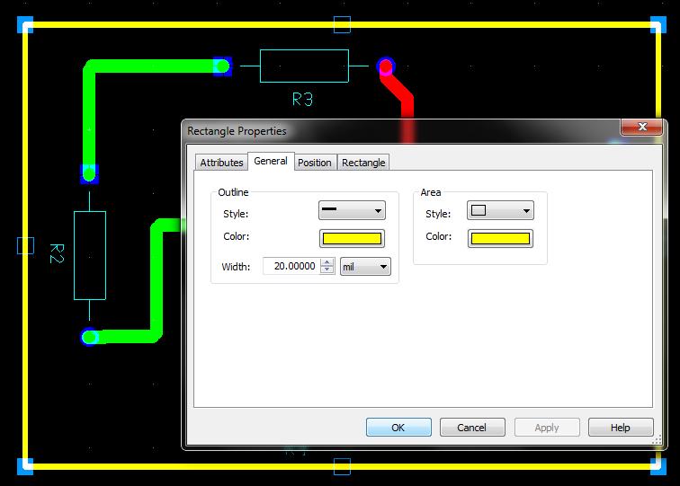
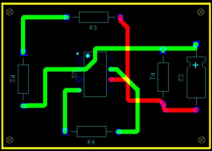
19 Cut Off Frequency 19
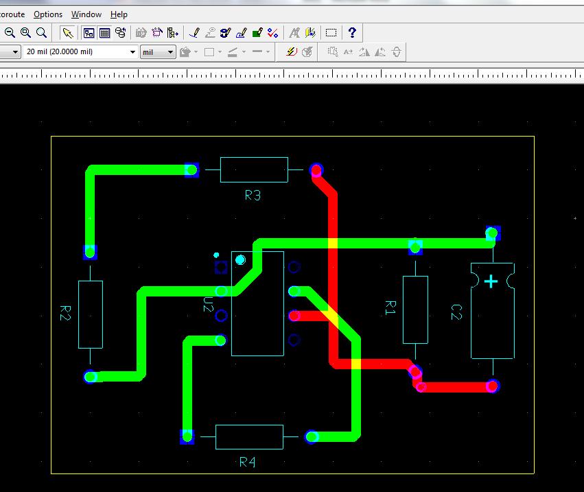
20 3dB Cut Off Frequency To find the LPF cut off frequency, you first need to select your cursors. You can do so by first clicking on the cursor item in your toolbar. The cursors will appear at the top of your Y-axis 1. Right-click on the green cursor arrow on your Y-axis 2. Select Set Y_Value => 3. A window pops and shows the current value of the Y- axis (in db). Subtract 3dB from this and type it in the field and click on OK 4. The cursor jumps to the cut off frequency. 5. You can select Grid by clicking on Grid Icon in Toolbar 20
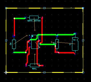
21 This LPF s cut off frequency is about 970 Hz 21


22 If instead of choosing Decibel we choose Linear for the vertical axis, the AC simulation produces the following magnitude response 22
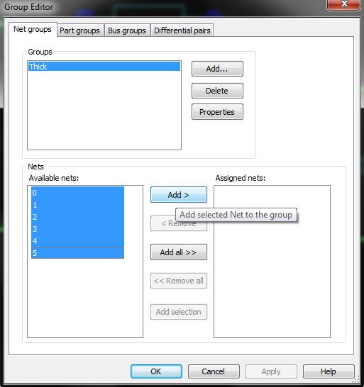
23 23
24 24
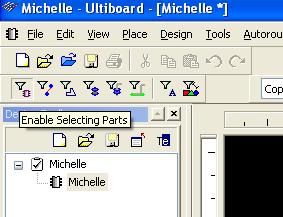
25 PCB Design in Ultiboard Before sending the schematic design from Multisim to Ultiboard we must have Footprint for all parts. (if parts are not blue, they don t have a footprint) Note: In schematic we must provision Input and Output pins to send a signal to the PCB and to measure the output. You can do this by creating in/out Jack or by using a resistor (explained later) Also the Op-amp must have a footprint associated with it 25
26 Using Resistor footprint as In/Out pins & Power Rails 26
27 As we mentioned all the BLUE color components have a footprint associated with them. Here ground is in BLACK We must create a jumper pin for it and attach pin 3 of OpAmp to it. We intentionally leave this unchanged, because we want to teach you how to manually route this pin to ground in Ultiboard. 27

28 Now we can transfer Multisim schematic to Ultiboard 28

29 29

30 30

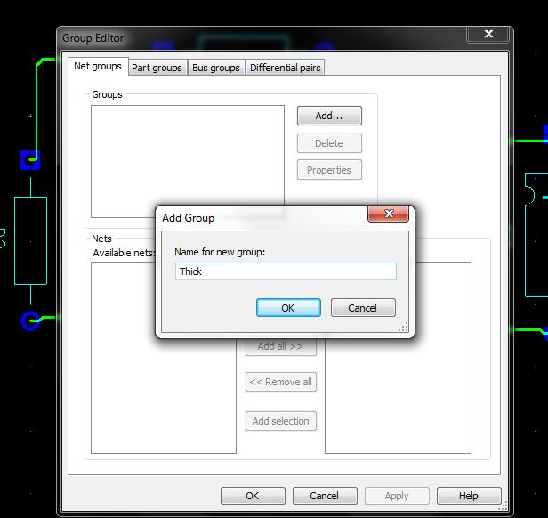
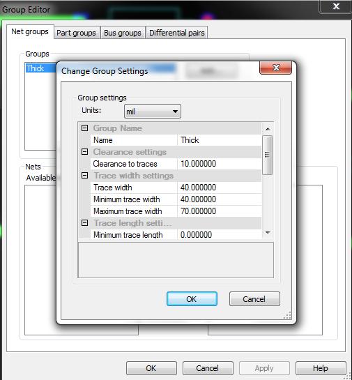
31 Changing Track width 31
32 32

33 33
34 34


35 Changing tracks from one layer to another 35
36 36
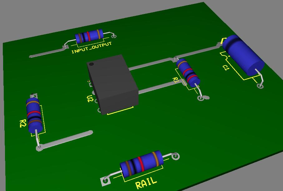
37 Creating Board Outline There is a minor difference in creating the Board Outline between Ultiboard v.12 and earlier versions So we will teach you the 2 techniques 37

38 Creating the Board Outline in Ultiboard v.12 38
39 39
40 40
41 41


42 Creating the Board Outline in Ultiboard other than v.12 42
43 43
")
44 Design Rule Check (DRC) 44


45 3D View 45
46 46

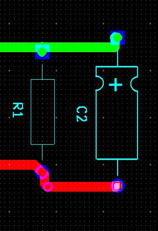
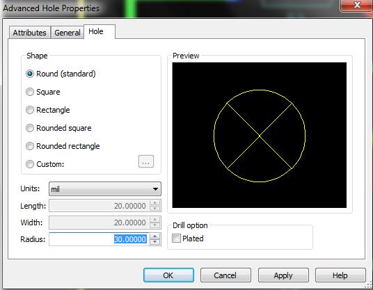
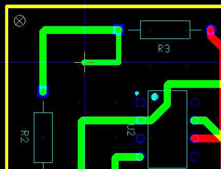
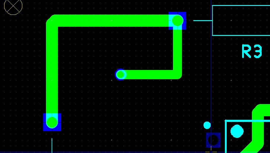
47 Placing Mounting Holes 47
48 48
49 49

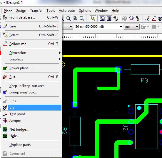
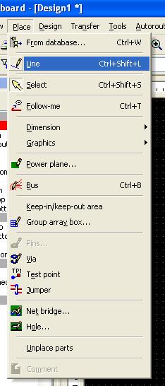
50 How to Manually Route a Trace 1. Choose a copper layer. 2. Select or enter the desired trace size in the Draw Settings toolbar. 3. Choose Place»Line. 4. Click a pad on the board. The net the pad is a part of is highlighted, and the pads in the net are each marked with an X. 5. Make your way to the next pad in the net remember to avoid parts and other traces. Click to fix the trace to the board each time you change direction. 50
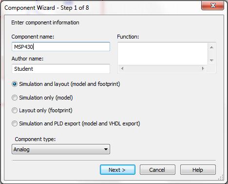
51 51

52 52
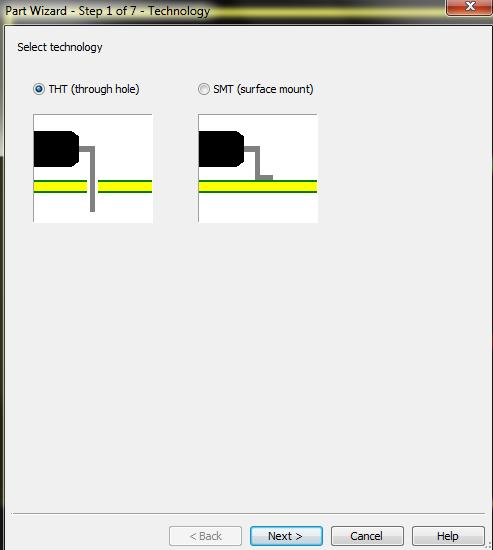
53 53

54 Now change Copper Top layer to Copper Bottom layer by highlighting it on Design Toolbox on the left hand side of the page 54

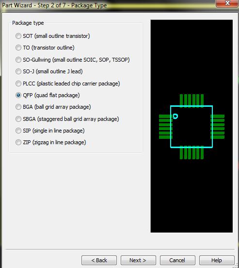
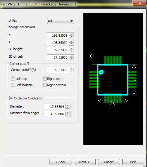
55 Choose Place»Line and draw a track connecting the VIA to the desired pin. 55
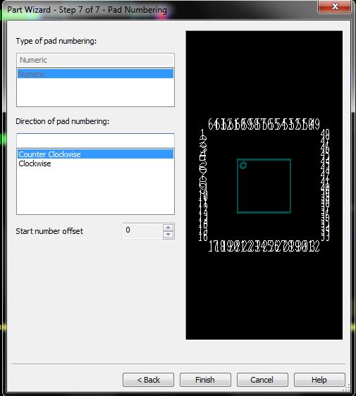
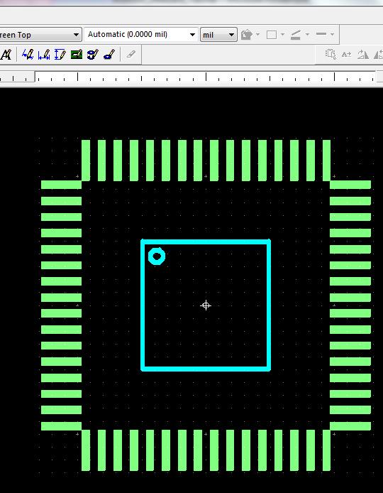
56 If you remember from earlier in Multisim we left out creating a jumper pin for GROUND Here we can manually route pin 3 of the OpAmp to create a ground Select Place Line Go on Pin3 and manually create a line (track) Route that track to a point on the corner of your PCB Add a VIA to the end (this would create a hole so you can solder a wire to it and use it as a common ground) 56

57 57
58 58
59 59

60 Creating NEW Parts in Multisim 60


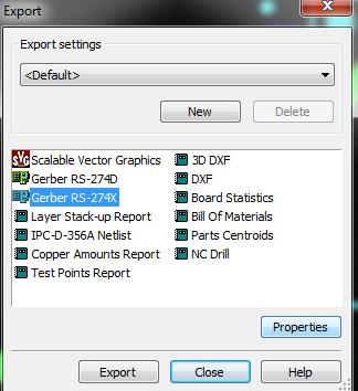
61 61

62 Creating NEW Footprint in Ultiboard 62
63 63
64 64
65 Suppose we want to create a footprint for our microcontroller MSP30F1611 from Texas Instrument. From MSP30F1611data sheet (or manual) we find the packaging is QFP (Quad Flat Package). 65
66 66

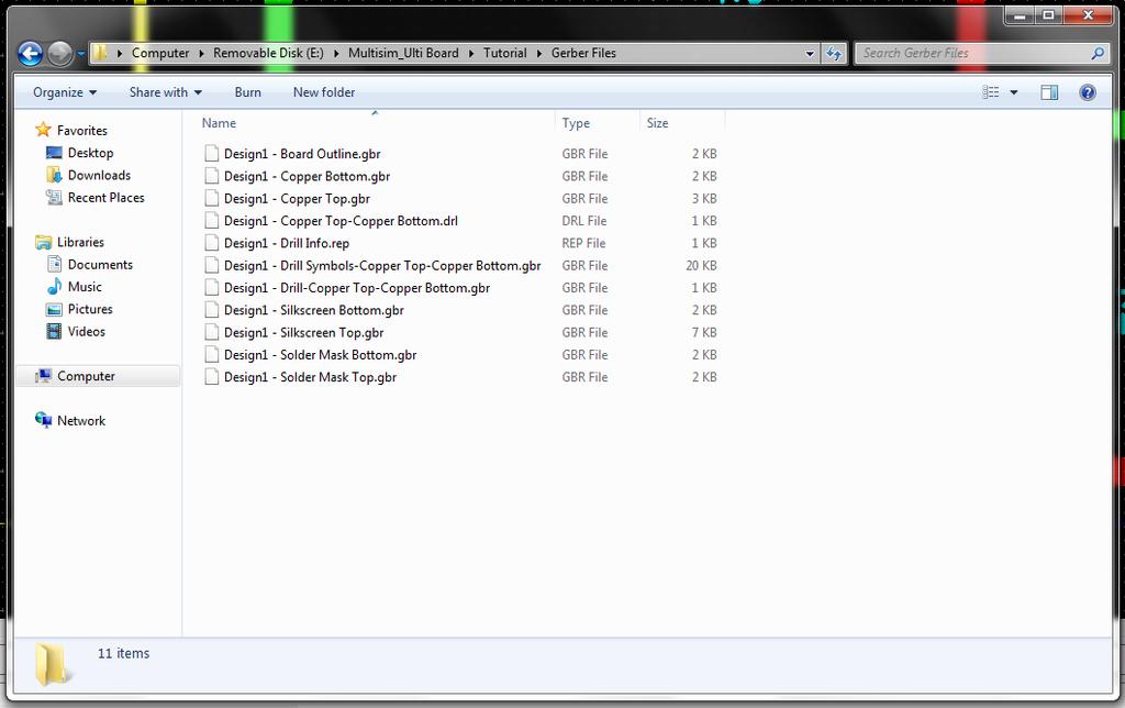
67 67
68 68
69 69
70 Exporting Gerber Files To begin generating the PCB files, the settings for each of the various file types will need to be established. The first files needed are the Gerber files which allow the manufacturer to create the basic artwork for each of the layers. From the menu: 1. Launch the Export setup window from the menu by selecting File > Export. 2. In the Export dialog box select the Gerber RS- 274X format 3. Click on the Properties button. 70
71 71
72 In the left side of the Gerber properties window, select the following Available Layers items and press the right-arrow to move them to the right-side window. 1. Board Outline 2. All copper layers (Copper Top, Copper Inner 1, Copper Inner 2, Copper Bottom, etc ) 3. Drill 4. Drill Symbols 5. Silkscreen Top and Silkscreen Bottom 6. Solder Mask Bottom and Solder Mask Top 72
 In the Digits section, select integer 2 and decimal place 4 Click OK.")
73 It is important to complete the following steps to finalize export: In the Units section select Imperial (Mil) In the Digits section, select integer 2 and decimal place 4 Click OK. 73
74 Creating Drill Files for PCB Manufacturer Next the Gerber and NC Drill files will need to be generated. The NC Drill files are reports indicating the hole sizes and locations for all holes within the design. 1. Launch the Export setup window from the menu by selecting File > Export. 2. In the Export dialog box select the NC Drill option 3. Click on the Properties button. 74

75 You will now be able to set the Drill Export properties. Generally the default options are appropriate for board manufacturers. 75
76 Export Gerbers and NC Drill Files To begin your final exporting process: 1. Select the Gerber RS-274X and NC Drill items by pressing the <Ctrl> key to select both items. 2. Press the Export button and multiple windows will open in sequence allowing each of the selected files to be saved. 3. For the first set of Gerber files an additional Create aperture mapping popup window will launch allowing the default D-code aperture settings to be changed; simply press OK to continue with the default settings. 4. Each Gerber layer (or merged layer) will generate a file with a.gbr extension and two NC drill files with a.drl and a.rep extension. 76

77 Once the save operation is completed, reorganize the files as required by the board manufacturer. Some manufacturers require the files to be zipped into a folder with a simple file naming format with just the layer names for each file type. For instance a file named SeniorDesignProject - Copper Top.gbr may need to be changed to Copper Top.gbr before sending. 77
78 78
79 1. The rep is a report file listing a summary of the drill sizes and quantities. 2. The drl file shows the exact locations of each hole. 3. In addition, there are two Gerber files that are related to PCB drilling. The Drill and Drill Symbols are created when the Gerber RS-274X is selected and subsequently these files are used in documentation such as the assembly drawing to verify all hole sizes and drill locations are correct. 4. The Drill Gerber file shows round images at each hole with the radius of the image the same as the hole radius. When viewing this layer, the user can observe the hole sizes, locations and relations to other locations on the PCB. 5. The Drill Symbols Gerber file has symbols shown for each tool. For example, if there are 5 different holes sizes needed for drilling into the PCB, there will be 5 different symbols on this Gerber layer. 79
80 Other open source software If the purpose is to create a PCB only (and no simulation is required), you can use other open source software such as 1. PCB Artist from Advanced Circuits ( 2. Eagle from CadSoft ( 80
81 Multisim User Manual: References 8C F2B51 Ultiboard User Manual: BC30AD C4D
2008 년안산일대디지털정보통신학과 CAD 강의용자료 PADS 2007
 2008 년안산일대디지털정보통신학과 CAD 강의용자료 PADS 2007 1 Learning the PADS User Interface What you will learn: Modeless Commands Panning & Zooming Object Selection Methods Note: This tutorial will use PADS Layout to
This section contains a tutorial that introduces you to Multisim and its many functions.
 GETTING STARTED GUIDE NI Circuit Design Suite This document contains the following step-by-step tutorials: Multisim Tutorial Multisim is the schematic capture and simulation program designed for schematic
TUTORIAL SESSION Technical Group Hoda Najafi & Sunita Bhide
 TUTORIAL SESSION 2014 Technical Group Hoda Najafi & Sunita Bhide SETUP PROCEDURE Start the Altium Designer Software. (Figure 1) Ensure that the Files and Projects tabs are located somewhere on the screen.
Exporting Gerber Files from NI Ultiboard
 Exporting Gerber Files from NI Ultiboard Overview When the design of a printed circuit board (PCB) is complete, the design needs to be sent to a PCB manufacturer to be physically fabricated. Rather than
Introduction to PCB Design with EAGLE. Jianan Li
 Introduction to PCB Design with EAGLE Jianan Li Install EAGLE Download EAGLE: http://www.cadsoftusa.com/download-eagle/ Choose Run as Freeware during installation Create a New Project Launch EAGLE and
Creating a PCB Design with OrCAD PCB Editor
 Creating a PCB Design with OrCAD PCB Editor This guide is focused on learning how to create a PCB (Printed Circuit board) design. The guide will make use of the PCB Flow menu that is part of this workshop
Tutorial : First board in CircuitMaker.
 Tutorial : First board in CircuitMaker. Objectives 1. Create a new project in CircuitMaker. 2. Design electronic circuit in CircuitMaker schematic editor. 3. Design a pcb board for your circuit in CircuitMaker
Orcad Layout Plus Tutorial
 Orcad Layout Plus Tutorial Layout Plus is a circuit board layout tool that accepts a layout-compatible circuit netlist (ex. from Capture CIS) and generates an output layout files that suitable for PCB
- create new schematic to the new project, PCB design begins with a schematic diagram, which present how components are connected
 Eagle 8.x tutorial - create a new project, Eagle designs are organized as projects - create new schematic to the new project, PCB design begins with a schematic diagram, which present how components are
Intro to Multisim & Ultiboard
 Intro to Multisim & Ultiboard (Lab by Wayne Stanton) Note: This document was written for version 13.0 of Multisim and Ultiboard. Note: A grade for this lab will be applied upon receipt of the project file.
Exercise 1. Section 2. Working in Capture
 Exercise 1 Section 1. Introduction In this exercise, a simple circuit will be drawn in OrCAD Capture and a netlist file will be generated. Then the netlist file will be read into OrCAD Layout. In Layout,
University of Kansas EECS Circuit Board Fabrication Tutorial for 212 Lab
 University of Kansas EECS Circuit Board Fabrication Tutorial for 212 Lab Preparing For Export... 1 Assigning Footprints... 1 Recommended Footprints... 2 No Connects... 3 Design Rules Check... 3 Create
Complete Tutorial (Includes Schematic & Layout)
") Complete Tutorial (Includes Schematic & Layout) Download 1. Go to the "Download Free PCB123 Software" button or click here. 2. Enter your e-mail address and for your primary interest in the product. (Your
Complete Tutorial (Includes Schematic & Layout) Download 1. Go to the "Download Free PCB123 Software" button or click here. 2. Enter your e-mail address and for your primary interest in the product. (Your
Lab 9 Introduction to Multisim & Ultiboard
 Lab 9 Introduction to Multisim & Ultiboard In this lab you will be utilizing your understanding of circuit generation/testing in Multisim in order to create the final project (figure 1), a TinyMatrix pendant.
Introduction Creating a Project Footprint Design
 EEC 134 Application Note Introduction to PCB Design Cameron Vossoughi Introduction Being fluent in PCB design is essential for electrical engineers regardless of their discipline focus. This application
ECEN 1400, Introduction to Analog and Digital Electronics
 ECEN 1400, Introduction to Analog and Digital Electronics How to create circuit boards using multisim and ultiboard This document walks you through the steps to make a working printed circuit board (PCB).
Procedure for PCBoard Layout
 Procedure for PCBoard Layout Introduction The following 6 pages of instructions will take you step by step through the creation of your PCB using Orcad Layout. If you are planning to manually lay out your
Tutorial 3: Using the Waveform Viewer Introduces the basics of using the waveform viewer. Read Tutorial SIMPLIS Tutorials SIMPLIS provide a range of t
 Tutorials Introductory Tutorials These tutorials are designed to give new users a basic understanding of how to use SIMetrix and SIMetrix/SIMPLIS. Tutorial 1: Getting Started Guides you through getting
Part. Summary. Modified by Susan Riege on Aug 5, Parent page: Objects
 Part Old Content - visit altium.com/documentation Modified by Susan Riege on Aug 5, 2016 Parent page: Objects Related Resources Net Ties and How to Use Them (PDF) The Part represents the actual physical
Getting started in the PCB Editor
 Getting started in the PCB Editor by Lori Zukerman of the EE/CAD group 01/07/04 Page 1 of 21 1. Initial Setup... 3 1.1 Copying Drawing Formats... 3 2. Starting your PCB... 3 2.1 Open a setup drawing...
Prototype PCBs design session
 Prototype PCBs design session By: Dr. Ahmed ElShafee ١ Dr. Ahmed ElShafee, ACU : Spring 2018, EEP04 Practical Applications in Electrical Before start You will be making a schematic (astable.sch) file which
Lab 9 PCB Design & Layout
 Lab 9 PCB Design & Layout ECT 224L Department of Engineering Technology Lab 9 PCB Traces Size dependent upon electrical requirements, design constraints (routing space and clearance), and trace/space resolution
Eagle use in Prototyping
 MICHIGAN STATE UNIVERSITY COLLEGE OF ENGINEERING Eagle use in Prototyping Eleazar Gutierrez 4/3/2015 Facilitator: Dr. Binseng Wang Design Team 12 Sponsor: MSU Solar Car Team Abstract In the development
Introduction to SolidWorks for Technology. No1: Childs Toy
 Introduction to SolidWorks for Technology No1: Childs Toy Table of Contents Table of Contents... 1 Introduction... 2 Part Modelling: Cab... 3 Part Modelling: Base... 6 Part Modelling: Wheel... 12 Assembly:
CADSOFT EAGLE TUTORIAL
 CADSOFT EAGLE TUTORIAL IEEE OPS 2013-2014 By Shubham Gandhi, Kamal Kajouke 1 Table of Contents 1. Introduction 1.1 Getting Started 1.2 Eagle Schematic Editor 1.3 The Toolbar and Command Bar 1.4 Importing
SCHEMATIC1 SCHEMATIC2 SCHEMATIC1 SCHEMATIC2 SCHEMATIC3 PAGE1 PAGE2 PAGE3 PAGE1 PAGE1 PAGE2 PAGE1 PAGE1 PAGE2
 An OrCAD Tutorial Dr. S.S.Limaye 1. Introduction OrCAD is a suite of tools from Cadence company for the design and layout of printed circuit boards (PCBs). This is the most popular tool in the industry.
Allegro PCB Editor with Performance Option or higher. The Reuse function can be used to create panels in PCB Editor
 Title: Product: Summary: Panelization with Reuse Allegro PCB Editor with Performance Option or higher The Reuse function can be used to create panels in PCB Editor Author/Date: Beate Wilke / 07.02.2011
Version Software Update Details Release Date 22-Sep Problem Fixes in Version
 Version 12.0.6 Software Update Details Release Date 22-Sep-2009 Problem Fixes in Version 12.0.6 This is the final roll-up patch for Version 12. No further updates will be issued for this version. Add Shape
KiCad Example Schematic ( ) Wien Bridge Oscillator
 Wien Bridge Oscillator") KiCad Example Schematic (2010-05-05) Wien Bridge Oscillator University of Hartford College of Engineering, Technology, and Architecture The following tutorial in that it walks you through steps to use
KiCad Example Schematic (2010-05-05) Wien Bridge Oscillator University of Hartford College of Engineering, Technology, and Architecture The following tutorial in that it walks you through steps to use
EE 210 Lab Assignment #2: Intro to PSPICE
 EE 210 Lab Assignment #2: Intro to PSPICE ITEMS REQUIRED None Non-formal Report due at the ASSIGNMENT beginning of the next lab no conclusion required Answers and results from all of the numbered, bolded
Start ADS and Create an Empty Project
 Start ADS and Create an Empty Project Look for a desktop icon or start menu item entitled Advanced Design System 2011 ADS will start up and you will see ultimately: ADS Session 1 click for new project
1. Working with PSpice:
 Applied Electronics, Southwest Texas State University, 1, 13 1. Working with PSpice: PSpice is a circuit simulator. It uses the Kirchhoff s laws and the iv-relation of the used components to calculate
1. Go to the project manager. 2. Select the line Lowpass filter.dsn and right click Part manager. Page 1 of 13
 Component management In you can easily manage components and their related information. Assembly variants and Bill of Materials (BOM) for these can also be defined. The built in Part Manager window makes
Lab 1: Analysis of DC and AC circuits using PSPICE
 Lab 1: Analysis of DC and AC circuits using PSPICE 1. Objectives. 1) Familiarize yourself with PSPICE simulation software environment. 2) Obtain confidence in performing DC and AC circuit simulation. 2.
Introduction to SolidWorks Basics Materials Tech. Wood
 Introduction to SolidWorks Basics Materials Tech. Wood Table of Contents Table of Contents... 1 Book End... 2 Introduction... 2 Learning Intentions... 2 Modelling the Base... 3 Modelling the Front... 10
Table of Contents. Part I Introduction. Part II Creating a simple Schematic and PCB. Part III Creating Libraries.
 TUTORIAL 2 DipTrace Tutorial Table of Contents Part I Introduction 4 Part II Creating a simple Schematic and PCB 4 1 Establishing a... schematic size and placing titles 5 2 Configuring libraries... 8 3
PADS-PowerPCB 4 Tutorial (with Blazeroute)
") PADS-PowerPCB 4 Tutorial (with Blazeroute) PADS-PowerPCB is the ultimate design environment for complex, high-speed printed circuit boards. PROCEDURE FOR SIMULATION IN SCHEMATICS 1. Importing Design Data
PADS-PowerPCB 4 Tutorial (with Blazeroute) PADS-PowerPCB is the ultimate design environment for complex, high-speed printed circuit boards. PROCEDURE FOR SIMULATION IN SCHEMATICS 1. Importing Design Data
Getting Started with PCB Design
 Getting Started with PCB Design Summary Tutorial TU0117 (v1.2) April 13, 2005 This introductory tutorial is designed to give you an overview of how to create a schematic, update the design information
PSpice with Orcad 10
 PSpice with Orcad 10 1. Creating Circuits Using PSpice Tutorial 2. AC Analysis 3. Step Response 4. Dependent Sources 5. Variable Phase VSin Source Page 1 of 29 Creating Circuits using PSpice Start Orcad
Lesson 5: Board Design Files
 5 Lesson 5: Board Design Files Learning Objectives In this lesson you will: Use the Mechanical Symbol Editor to create a mechanical board symbol Use the PCB Design Editor to create a master board design
Construction of Industrial Electronic Equipments
 VSB-Technical university of Ostrava Faculty of Electrical Engineering and Computer Science Department of electronics Construction of Industrial Electronic Equipments Syllabus Part 2 PCB Design and Fabrication
MAKE A PRINTED-CIRCUIT-BOARD (PCB) FOR YOUR ELECTRONIC DEVICE 11/10/2017 CLIFF CURRY
 FOR YOUR ELECTRONIC DEVICE 11/10/2017 CLIFF CURRY") MAKE A PRINTED-CIRCUIT-BOARD (PCB) FOR YOUR ELECTRONIC DEVICE 11/10/2017 CLIFF CURRY PART ONE: AN INTRODUCTION TO PRINTED CIRCUIT BOARDS. WHAT ARE THEY, AND HOW DOES ONE SPECIFY THEM TO GET WHAT ONE WANTS?
MAKE A PRINTED-CIRCUIT-BOARD (PCB) FOR YOUR ELECTRONIC DEVICE 11/10/2017 CLIFF CURRY PART ONE: AN INTRODUCTION TO PRINTED CIRCUIT BOARDS. WHAT ARE THEY, AND HOW DOES ONE SPECIFY THEM TO GET WHAT ONE WANTS?
Electronics Design - Eagle
 Back to tutorial index Electronics Design - Eagle This week's assignment is to: add a button and LED to the echo hello-world board, check the design rules, and make it. Review Neil's class page: http://academy.cba.mit.edu/classes/electronics_design/index.html
Using OrCAD Layout Plus A Simple Guide
 Using OrCAD Layout Plus A Simple Guide Written by Jose Cabral September 2006 Revised by Nithin Raghunathan 1 SKETCH THE CIRCUIT YOU WISH TO LAYOUT SKETCH THE LAYOUT COM J1 OUTPUT +12 COM -12 COM INPUT
Lab 4: Digital Electronics Innovation Fellows Program Boot Camp Prof. Steven S. Saliterman
 Lab 4: Digital Electronics Innovation Fellows Program Boot Camp Prof. Steven S. Saliterman Exercise 4-1: Familiarization with Lab Box Contents & Reference Books 4-1-1 CMOS Cookbook (In the bookcase in
Click on the SwCAD III shortcut created by the software installation.
 LTSpice Guide Click on the SwCAD III shortcut created by the software installation. Select File and New Schematic. Add a component Add a resistor Press R or click the resistor button to insert a resistor.
PCB Design utilizing Cadence Software. Application Note
 PCB Design utilizing Cadence Software Application Note Kyle Schultz 11-9-11 ECE 480 Design Team 5 Keywords: Schematic, PCB, Fabrication, Cadence, Design Entry CIS, Allegro Table of Contents Abstract 1
Lecture 14: Prototyping and Schematics
 Lecture 14: Prototyping and Schematics Breadboards have some limitations They have high parasitic inductance and capacitance, limiting high frequency signal transfer to about 50MHz. Wire connections
Lab 4: Digital Electronics BMEn 2151 Introductory Medical Device Prototyping Prof. Steven S. Saliterman
 Lab 4: Digital Electronics BMEn 2151 Introductory Medical Device Prototyping Prof. Steven S. Saliterman Exercise 4-1: Familiarization with Lab Box Contents & Reference Books 4-1-1 CMOS Cookbook (In the
Gerber files. EE 333 Gerber files 1
 Gerber files To have our design turned into a PCB we need to send the it to a manufacturer. There are many choices, but for EE 333, our default vendor will be Oshpark. (oshpark.com) Depending on board
Getting started. Starting Capture. To start Capture. This chapter describes how to start OrCAD Capture.
 Getting started 1 This chapter describes how to start OrCAD Capture. Starting Capture The OrCAD Release 9 installation process puts Capture in the \PROGRAM FILES\ORCAD\CAPTURE folder, and adds Pspice Student
Designing a PCB using EagleCAD
 Designing a PCB using EagleCAD Atlanta Hobby Robot Club Yes, you can design your own custom PCB and this tutorial will show you how. It is easier than ever to design your own PCB and having it manufactured
Experiment 1 Electrical Circuits Simulation using Multisim Electronics Workbench: An Introduction
 Experiment 1 Electrical Circuits Simulation using Multisim Electronics Workbench: An Introduction Simulation is a mathematical way of emulating the behavior of a circuit. With simulation, you can determine
Nordcad Flow menus. Rev Nordcad Systems A/S
 Nordcad Flow menus Rev 1.00 2014 Nordcad Systems A/S www.nordcad.dk Support@nordcad.dk Purpose The purpose of the PCB and Footprint flow menus is to guide the user through a number of steps normally involved
1. Move your mouse to the location you wish text to appear in the document. 2. Click the mouse. The insertion point appears.
 Word 2010 Text Basics Introduction Page 1 It is important to know how to perform basic tasks with text when working in a word processing application. In this lesson you will learn the basics of working
Bold is used for UI elements that will appear on screen (buttons, menus or menu items, etc.)
") PCB Workshop Notes 26 November 2015 Tutorial References (presentation, sample project): http://ieee.concordia.ca/portfolio/pcb workshop/ Vocabulary & Concepts Software: DipTrace, in this case Packages:
PCB Workshop Notes 26 November 2015 Tutorial References (presentation, sample project): http://ieee.concordia.ca/portfolio/pcb workshop/ Vocabulary & Concepts Software: DipTrace, in this case Packages:
OrCad & Spice Tutorial By, Ronak Gandhi Syracuse University
 OrCad & Spice Tutorial By, Ronak Gandhi Syracuse University Brief overview: OrCad is a suite of tools from Cadence for the design and layout of circuit design and PCB design. We are currently using version
DipTrace Tutorial Table of Contents Part I Introduction Part II Creating a simple Schematic and PCB
 TUTORIAL 2 DipTrace Tutorial Table of Contents Part I Introduction 4 Part II Creating a simple Schematic and PCB 4 1 Establishing... schematic size and placing titles 5 2 Configuring... libraries 9 3 Designing...
Orcad Tutorial: Oscillator design and Simulation Schematic Design and Simulation in Orcad Capture CIS Full Version
 Orcad Tutorial: Oscillator design and Simulation Prof. Law Schematic Design and Simulation in Orcad Capture CIS Full Version Notation: To simplify what one should click to perform a task, the following
Using EAGLE: Schematic a learn.sparkfun.com
 Using EAGLE: Schematic a learn.sparkfun.com tutorial Available online at: http://sfe.io/t109 Contents Introduction Create a Project Adding Parts to a Schematic Wiring Up the Schematic Tips and Tricks Resources
EECS 211 CAD Tutorial. 1. Introduction
 EECS 211 CAD Tutorial 1. Introduction This tutorial has been devised to run through all the steps involved in the design and simulation of an audio tone control amplifier using the Mentor Graphics CAD
Design capture, simulation and layout - an introduction Tutorial
 Design capture, simulation and layout - an introduction Tutorial A step-by-step introduction to Altium s complete board-level design system 1 Software, documentation and related materials: Copyright 2002
Workshop 5-1: Dynamic Link
 Workshop 5-1: Dynamic Link 2015.0 Release ANSYS HFSS for Antenna Design 1 2015 ANSYS, Inc. Overview Linear Circuit Overview Dynamic Link Push Excitations Dynamic Link Example: Impedance Matching of Log-Periodic
EAGLE 6.x.x. University of Applied Sciences Ravensburg-Weingarten. EAGLE Tutorial. Author: Christian Schmid
 University of Applied Sciences Ravensburg-Weingarten EAGLE Tutorial EAGLE 6.x.x Author: Christian Schmid christian.schmid@hsweingarten.de Author: Martin Meier martin.meier@hs-weingarten.de September 30,
Lesson 9: Advanced Placement Techniques
 9 Lesson 9: Advanced Placement Techniques Learning Objectives In this lesson you will: Turn ratsnests on and off to selectively place components Use interactive swapping for pins and gates Apply advanced
Pads are used to provide both mechanical mounting and electrical connections to the component pins.
 Pad Old Content - visit altium.com/documentation Modified by Jason Howie on 19-Aug-2015 Parent page: Objects Pads are used to provide both mechanical mounting and electrical connections to the component
Simulation examples Chapter overview
 Simulation examples 2 Chapter overview The examples in this chapter provide an introduction to the methods and tools for creating circuit designs, running simulations, and analyzing simulation results.
Lesson 17: Building a Hierarchical Design
 Lesson 17: Building a Hierarchical Design Lesson Objectives After you complete this lesson you will be able to: Explore the structure of a hierarchical design Editing the Training Root Schematic Making
Revision Notes: July2004 Generate tutorial for single transistor analysis. Based on existing schematic entry tutorial developed for ECE410
 Cadence Analog Tutorial 1: Schematic Entry and Transistor Characterization Created for the MSU VLSI program by Professor A. Mason and the AMSaC lab group. Revision Notes: July2004 Generate tutorial for
Instructions for designing the HelloWorld circuit board using Autodesk Eagle 8.6.0
 Instructions for designing the HelloWorld circuit board using Autodesk Eagle 8.6.0 FABLAB BRIGHTON 2018 These instructions take you through step-by-step the process of creating the full circuit board design
A Quick EAGLE PCB Tutorial
 A Quick EAGLE PCB Tutorial Tim Steffes Mark Brehob 9/17/11 Introduction So, you ve finished your circuit prototype and you re ready to make it permanent? Tired of those messy wires and loose components,
Getting Started with Orcad Lite, Release 9.2
 Getting Started with Orcad Lite, Release 9.2 Professor Robert Hofinger Purdue University - Columbus You start a new project (program) by going to the File menu in the upper left corner, then New, and then
Department of Electrical and Electronics Engineering SSN College of Engineering
 1 Department of Electrical and Electronics Engineering SSN College of Engineering 2 TABLE OF CONTENTS EAGLE CADSOFT Professional 2 Getting Started 3 Toolbar quick reference 5 Creating the Schematic 6 Creating
EXPERIMENT 1 INTRODUCTION TO MEMS Pro v5.1: DESIGNING a PIEZO- RESISTIVE PRESSURE SENSOR
 EXPERIMENT 1 INTRODUCTION TO MEMS Pro v5.1: DESIGNING a PIEZO- RESISTIVE PRESSURE SENSOR 1. OBJECTIVE: 1.1 To learn and get familiar with the MEMS Pro environment and tools 1.2 To learn the basis of process
There are three windows that are opened. The screen that you will probably spend the most time in is the SCHEMATIC page.
 Pspice Tutorial Create a new project and select Analog or Mixed A/D. Choose an appropriate project name and a path. A new window pop up with the Pspice project type, select Create a blank project and click
Autodesk Inventor Design Exercise 2: F1 Team Challenge Car Developed by Tim Varner Synergis Technologies
 Autodesk Inventor Design Exercise 2: F1 Team Challenge Car Developed by Tim Varner Synergis Technologies Tim Varner - 2004 The Inventor User Interface Command Panel Lists the commands that are currently
5 When creating a Thermal Pad you should determine the size of your WebClear (Air-Gap) first, usually 10 th (mils) would have been sufficed.
 first, usually 10 th (mils) would have been sufficed.") APPENDIX A SMD AND MULTI-LAYERED PAD Creating SMD Pad and Multi-Layered Pad are generally the same as the pads that you create in Lab 3 with only a slight difference in layer assignment. Multi-Layered
APPENDIX A SMD AND MULTI-LAYERED PAD Creating SMD Pad and Multi-Layered Pad are generally the same as the pads that you create in Lab 3 with only a slight difference in layer assignment. Multi-Layered
Release Highlights for CAM350 Product Version 10.7
 Release Highlights for CAM350 Product Version 10.7 Introduction CAM350 Version 10.7 is a support release that introduces new functionality, including encryption of CAM350 macros. New Functionality The
Lesson 11: Interactive Routing and Glossing
 11 Lesson 11: Interactive Routing and Glossing Learning Objectives In this lesson you will: Define and display etch grids used for routing Create via fanouts Add and delete connect lines (clines) and vias
Interactive 3D Measurement Tool
 Published on Online Documentation for Altium Products (https://www.altium.com/documentation) Home > 3D Measurements Using Altium Documentation Modified by Jason Howie on Apr 11, 2017 Interactive 3D Measurement
Figure 1: ADE Test Editor
 Due to some issues that ADE GXL simulation environment has (probably because of inappropriate setup), we will run simulations in the ADE L design environment, which includes all the necessary tools that
HOW TO MAKE PCB USING CIRCUITCAM AND BOARDMASTER
 HOW TO MAKE PCB USING CIRCUITCAM AND BOARDMASTER This tutorial explains how to make a PCB using CircuitCAM and BoardMaster using the Gerber files of a design. First let s open CircuitCAM program. We can
Moving to Altium Designer from Pads Logic and PADS Layout
 Moving to Altium Designer from Pads Logic and PADS Layout Old Content - visit altium.com/documentation Modified by on 13-Sep-2017 Translating complete PADS Logic and PADS Layout designs, including PCB,
SOUTHERN POLYTECHNIC S. U.
 SOUTHERN POLYTECHNIC S. U. ECET 1012 Laboratory Exercise #4 ELECTRICAL & COMPUTER ENGINEERING TECHNOLOGY Introduction to PSpice Name Lab Section Date Overview: This laboratory experiment introduces the
EAGLE Schematic Software Cornerstone Electronics Technology and Robotics II
 EAGLE Schematic Software Cornerstone Electronics Technology and Robotics II Administration: o Prayer EAGLE Light Edition: o The name EAGLE is an acronym which stands for Easily Applicable Graphical Layout
High Power (15W + 15W) Stereo Amplifier
 Stereo Amplifier") High Power (15W + 15W) Stereo Amplifier Build Instructions Issue 1.0 Build Instructions Before you put any components in the board or pick up the soldering iron, just take a look at the Printed Circuit
High Power (15W + 15W) Stereo Amplifier Build Instructions Issue 1.0 Build Instructions Before you put any components in the board or pick up the soldering iron, just take a look at the Printed Circuit
GETTING STARTED WITH ADS
 ADS Startup Tutorial v2 Page 1 of 17 GETTING STARTED WITH ADS Advanced Design System (ADS) from Agilent Technologies is an extremely powerful design tool for many aspects of electrical and computer engineering
Introducing Eagle PCB
 ETH Course 402 0248 00L: Electronics for Physicists II (Digital) 1: Setup uc tools, introduction 2: Solder SMD AVR32 board 3: Build application around AVR32 4: Design your own PCB schematic 5: Place and
Lesson 11: Routing and Glossing
 11 Lesson 11: Routing and Glossing Learning Objectives In this lesson you will: Define and display etch grids used for routing Create via fanouts Add and delete connect lines (clines) and vias Use Slide
Preparing the Board for Design Transfer. Creating and Modifying the Board Shape. Modified by Phil Loughhead on 15-Aug-2016
 Preparing the Board for Design Transfer Old Content - visit altium.com/documentation Modified by Phil Loughhead on 15-Aug-2016 This article describes how to prepare the new PCB file so that it is ready to
An OrCAD Tutorial for ELEC 424 High-Speed Systems Design Revision Spring 2002
 An OrCAD Tutorial for ELEC 424 High-Speed Systems Design Revision 1.0 - Spring 2002 An OrCAD Tutorial An OrCAD Tutorial Page 2 of 55 1. Introduction OrCAD is a suite of tools from Cadence for the design
BehringerMods.com. Instructions for modification of Behringer SRC analog inputs and outputs
 BehringerMods.com Instructions for modification of Behringer SRC analog inputs and outputs The following instructions will cover the details of fully modifying a unit with analog output and analog input
The EAGLE Schematic & PCB Layout Editor - A Guide
 The EAGLE Schematic & PCB Layout Editor - A Guide Tom Clarke, v1.03 c Imperial College London, 2005, 2006, 2007, 2008, 2011,2012 November 9, 2012 (a) Dual in line package (b) Surface mount device Figure
Analog IC Simulation. Mentor Graphics 2006
 Analog IC Simulation Mentor Graphics 2006 Santa Clara University Department of Electrical Engineering Date of Last Revision: March 29, 2007 Table of Contents 1. Objective... 3 2. Basic Test Circuit Creation...
Board Options. Modified by Phil Loughhead on 27-Jan Parent page: PCB Dialogs. Old Content - visit altium.com/documentation
 Board Options Old Content - visit altium.com/documentation Modified by Phil Loughhead on 27-Jan-2016 Parent page: PCB Dialogs The Board Options Dialog. Summary Board Options dialog allows the designer
Tutorial - Getting Started with PCB Design
 Tutorial - Getting Started with PCB Design Old Content - visit altium.com/documentation Modified by Phil Loughhead on 3-Aug-2016 Welcome to the world of electronic product development environment in Altium
INTRODUCTION... 3 PRICE... 3 COMPATIBILITY... 5 INSTALLATION...
 xcheck Version 2.3 Table of Contents INTRODUCTION... 3 PRICE... 3 COMPATIBILITY... 5 INSTALLATION... 5 PROGRAM INSTALLATION... 5 INSTALLING.NET... 5 APPLICATION OVERVIEW... 6 TUTORIAL... 7 PERFORM ANALYSIS...
Altium Encoder Demo. Step 1 - Create a Polar Grid
 Altium Encoder Demo Note: In this tutorial I have used metric units. Altium defaults to Imperial units, you can change to metric once you have started a new PCB by selecting DESIGN>BOARD OPTIONS and then
A Crash Course on Using Agilent Advanced Design System (ADS)
") A Crash Course on Using Agilent Advanced Design System (ADS) By Chris Sanabria, sanabria@ece.ucsb.edu 2/9/02 If you are an engineer and have anything to do with circuit simulation, in particular high frequency
A Crash Course on Using Agilent Advanced Design System (ADS) By Chris Sanabria, sanabria@ece.ucsb.edu 2/9/02 If you are an engineer and have anything to do with circuit simulation, in particular high frequency
ECE383: Microprocessors Lab 9 Analog-to-Digital and Digital-to-Analog Conversion with I 2 C Serial EEPROM Data Storage
 ECE383: Microprocessors Lab 9 Analog-to-Digital and Digital-to-Analog Conversion with I 2 C Serial EEPROM Data Storage Goals: The goals of this lab are to introduce students to a PIC24-based hardware system