Prototype PCBs design session
|
|
|
- Jemima Carr
- 5 years ago
- Views:
Transcription


1 Prototype PCBs design session By: Dr. Ahmed ElShafee ١ Dr. Ahmed ElShafee, ACU : Spring 2018, EEP04 Practical Applications in Electrical
2 Before start You will be making a schematic (astable.sch) file which contains your circuit diagram & a PCB board layout (astable.brd) file. Each file has its own editor window. At any time you will change just one of these but the two are linked, so that the connections & components on the schematic always exist on the board. For example if you try to delete components on the board you will be asked to make the change on the schematic first. To undo command (Edit >Undo or Ctrl Z) to refresh the display View >Redraw (F2) ٢

3 Start the EAGLE control panel. Options >Directories gives a list of directories. Change the projects directory if necessary to something convenient that you can write, e.g. ٣
4 All new projects will be created inside this directory, and the EAGLE project navigator in the control panel uses this as a root. ٤

5 Schematic Creation Start the EAGLE Control Panel application. Create a new project: File >New >Project. ٥
6 ٦
7 Rename the project if you wish as follows: the control panel window indicates whether a project is open with a green circle next to the project name. Click this if necessary to close the project. Then Right click >Rename on the project's name. After having renamed the project you can reopen it. ٧

8 Right click on the Project name >New >Schematic. The schematic window will open. Inside the schematic window: ٨


9 File >Save as (choose a suitable name for your schematic sheet ٩

10 ١٠

11 ١١

12 Add components to your schematic: Edit >Add > Select component. ١٢

13 Click on add icon ١٣

14 ١٤

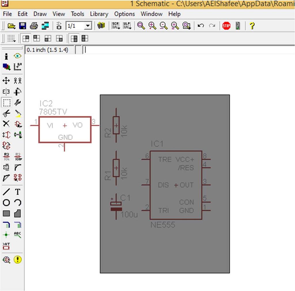
15 ١٥

16 ١٦


17 Left click to place each component. Right click before placing to rotate the component. Any number of the selected component can be added. To stop the ADD procedure select Edit >Stop Command. ١٧


18 Press esc to end add command ١٨


19 components can also be moved after adding, with the Edit >Move command, ١٩


20 or rotated with the Edit >Rotate command. ٢٠

21 Copy, delete ٢١
22 Rest of components used in astable circuit Name Library Device Package Electrolytic cap 220uF rcl > CPOL-EU CPOL-EUE E5-10,5 Resistors 1/4W normal fit rcl > R-EU_ R-EU_0207/ /10 ٢٢


23 ٢٣
24 ٢٤
25 ٢٥

26 Change value ٢٦

27 ٢٧

28 ٢٨

29 move block ٢٩

30 ٣٠

31 ٣١
32 Add more components Name Library Device Package 78xx Voltage regulator linear > 78* 7805TV TO220V Vertical Power socket Con-jack DCJ0202 DCJ0202 LED 5mm Led > LED > LED5MM LED5MM ٣٢
33 ٣٣

34 Add supply ٣٤

35 ٣٥


36 ٣٦

37 Connecting components using net ٣٧
38 ٣٨
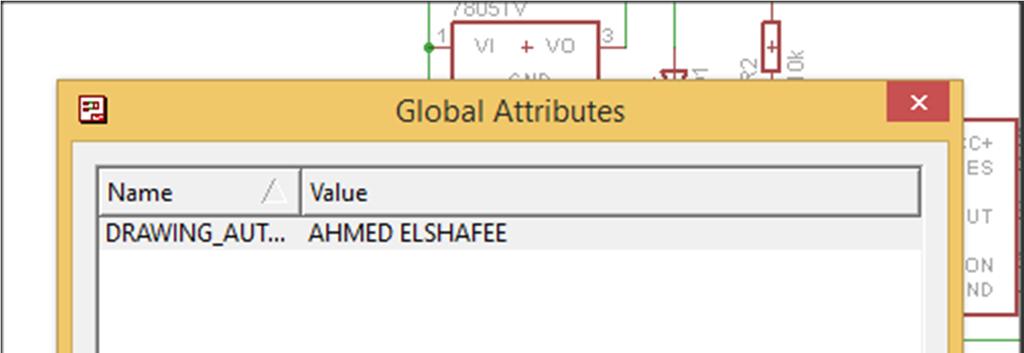
39 Where a wire joins the middle of another there must be a green circle (Draw >Junction) to indicate connection. Sometimes two nets are adjacent and appear joined but in fact are not. The View >Show tool () is invaluable here. If you click on any part of a net it will highlight all connected wires and component endpoints. You can then easily check what is missing. When you encounter such an error simply delete (Edit >Delete) line segments around the problem and rewire again (Draw >Net). ٣٩

40 ٤٠
41 Electrical Rule Check When you think you have connected everything you must do an ERC which will identify disconnected pins, nets which are next to each other but not connected, etc. Tools >ERC ٤١


42 ٤٢

43 ٤٣

44 ٤٤

45 ٤٥

46 Add docfield: ٤٦

 will update the")
47 Edit >Global attributes >New and add name=drawing_author, value= <your text>. View >Redraw (F2) will update the displayed text as in Figure 5. ٤٧

48 ٤٨

 with File >Export")
49 Printing a Parts List : You can print a parts list for a schematic (including resistor and capacitor values) with File >Export >Partslist. ٤٩


50 ٥٠

51 ٥١


52 Board Creation & Layout File >Switch to Board ٥٢
 which represents the board area.")
53 The board consists of all your components, with connections shown as a ratsnest, and a rectangular wire outline (default 100mmX80mm) which represents the board area. ٥٣
54 You can do this any time, but it is easier before you have populated the board outline. The wire rectangle defines where the board will be cut. To change the board size Edit >Move and left click near the middle of the top or right side of the rectangle to pick it up. Re position making sure the board stays rectangular, and left click again to terminate. Don t ever reposition the bottom or left sides, which should intersect very near the origin cross. ٥٤


55 ٥٥
56 Position the components inside the board outline Move the components one by one inside the rectangular board outline (Edit >Move) and position them where you want. Note that you must move components into the allowed 100*80mm area and cannot rearrange them outside the allowed area ٥٦

57 ٥٧
58 ٥٨
59 Use EEE custom DRC and autoroute parameters In order for board manufacture to allow easy soldering we need to make pads bigger by changing the default DRC rules File Allows you to pick which DRC file to use. Layers layers can be added by changing Setup to be something like (1*2*15*16) Clearance This tells Eagle how much room you want between the different types of electrical contacts on the board. 20 Dr. mils Ahmed ElShafee, is a reasonable ACU : Spring 2018, EEP04 clearance. Practical Applications in Electrical ٥٩

60 ٦٠
61 Distance Copper/Dimension is the distance from any routing to the edge of the board. Drill/Hole is the distance from any routing to a hole in the board. Sizes Set the minimum sizes. ٦١


62 ٦٢
63 Restring Restring controls the size of the through hole pads/vias. Typically I just leave these at their default values. Shapes Allows you to make pads have rounded edges. Typically I don't touch this one either. Supply The checkbox allows you to turn on thermals for vias, and Thermal Isolation lets you pick the length of the thermal traces. Typically I don't touch these values at all. ٦٣
64 Masks When PCBs are fabricated, they have a coating that covers and insulates all of the board, except for areas designated by the stop mask. After fabrication, if they are being assembled by a machine (or a person with a reflow oven), a stencil is created and solder paste is applied via that stencil to the pads/vias that need to be soldered. Stop controls the size of the openings in the stop mask for the various parts, and Cream controls the size of the openings in the stencil. Once again, the default values work just fine for our typical usage. ٦٤

65 DRC check ٦٥


66 ٦٦

67 Rotate and move some components ٦٧

68 ratsnest ٦٨


69 Auto route ٦٩
70 After auto route ٧٠


71 Add missing wires on top layer ٧١

72 Another trial ٧٢


73 ٧٣


74 ٧٤


75 And that s the manual solution ٧٥
76 AStable PCB ٧٦


77 ٧٧
78 MonoStable PCB ٧٨


79 ٧٩
80 Thanks,.. ٨٠ Dr. Ahmed ElShafee, ACU : Spring 2018, EEP04 Practical Applications in Electrical
Eagle use in Prototyping
 MICHIGAN STATE UNIVERSITY COLLEGE OF ENGINEERING Eagle use in Prototyping Eleazar Gutierrez 4/3/2015 Facilitator: Dr. Binseng Wang Design Team 12 Sponsor: MSU Solar Car Team Abstract In the development
- create new schematic to the new project, PCB design begins with a schematic diagram, which present how components are connected
 Eagle 8.x tutorial - create a new project, Eagle designs are organized as projects - create new schematic to the new project, PCB design begins with a schematic diagram, which present how components are
Introduction to PCB Design with EAGLE. Jianan Li
 Introduction to PCB Design with EAGLE Jianan Li Install EAGLE Download EAGLE: http://www.cadsoftusa.com/download-eagle/ Choose Run as Freeware during installation Create a New Project Launch EAGLE and
Lecture 14: Prototyping and Schematics
 Lecture 14: Prototyping and Schematics Breadboards have some limitations They have high parasitic inductance and capacitance, limiting high frequency signal transfer to about 50MHz. Wire connections
The EAGLE Schematic & PCB Layout Editor - A Guide
 The EAGLE Schematic & PCB Layout Editor - A Guide Tom Clarke, v1.03 c Imperial College London, 2005, 2006, 2007, 2008, 2011,2012 November 9, 2012 (a) Dual in line package (b) Surface mount device Figure
CADSOFT EAGLE TUTORIAL
 CADSOFT EAGLE TUTORIAL IEEE OPS 2013-2014 By Shubham Gandhi, Kamal Kajouke 1 Table of Contents 1. Introduction 1.1 Getting Started 1.2 Eagle Schematic Editor 1.3 The Toolbar and Command Bar 1.4 Importing
Construction of Industrial Electronic Equipments
 VSB-Technical university of Ostrava Faculty of Electrical Engineering and Computer Science Department of electronics Construction of Industrial Electronic Equipments Syllabus Part 2 PCB Design and Fabrication
HW #2 - Eagle Tutorial
 HW #2 - Eagle Tutorial The goal of this homework is to teach the user the basic steps of producing a switching power supply schematic and a printed circuit board using the Eagle Application. While tutorial
Designing a PCB using EagleCAD
 Designing a PCB using EagleCAD Atlanta Hobby Robot Club Yes, you can design your own custom PCB and this tutorial will show you how. It is easier than ever to design your own PCB and having it manufactured
EAGLE 6.x.x. University of Applied Sciences Ravensburg-Weingarten. EAGLE Tutorial. Author: Christian Schmid
 University of Applied Sciences Ravensburg-Weingarten EAGLE Tutorial EAGLE 6.x.x Author: Christian Schmid christian.schmid@hsweingarten.de Author: Martin Meier martin.meier@hs-weingarten.de September 30,
Complete Tutorial (Includes Schematic & Layout)
") Complete Tutorial (Includes Schematic & Layout) Download 1. Go to the "Download Free PCB123 Software" button or click here. 2. Enter your e-mail address and for your primary interest in the product. (Your
Complete Tutorial (Includes Schematic & Layout) Download 1. Go to the "Download Free PCB123 Software" button or click here. 2. Enter your e-mail address and for your primary interest in the product. (Your
Instructions for designing the HelloWorld circuit board using Autodesk Eagle 8.6.0
 Instructions for designing the HelloWorld circuit board using Autodesk Eagle 8.6.0 FABLAB BRIGHTON 2018 These instructions take you through step-by-step the process of creating the full circuit board design
Introduction to NI Multisim & Ultiboard
 George Washington University School of Engineering and Applied Science Electrical and Computer Engineering Department Introduction to NI Multisim & Ultiboard Dr. Amir Aslani 8/20/2017 2 Outline Design
Exercise 1. Section 2. Working in Capture
 Exercise 1 Section 1. Introduction In this exercise, a simple circuit will be drawn in OrCAD Capture and a netlist file will be generated. Then the netlist file will be read into OrCAD Layout. In Layout,
A Quick EAGLE PCB Tutorial
 A Quick EAGLE PCB Tutorial Tim Steffes Mark Brehob 9/17/11 Introduction So, you ve finished your circuit prototype and you re ready to make it permanent? Tired of those messy wires and loose components,
Electronics Design - Eagle
 Back to tutorial index Electronics Design - Eagle This week's assignment is to: add a button and LED to the echo hello-world board, check the design rules, and make it. Review Neil's class page: http://academy.cba.mit.edu/classes/electronics_design/index.html
Getting Started with PCB Design
 Getting Started with PCB Design Summary Tutorial TU0117 (v1.2) April 13, 2005 This introductory tutorial is designed to give you an overview of how to create a schematic, update the design information
Creating a PCB Design with OrCAD PCB Editor
 Creating a PCB Design with OrCAD PCB Editor This guide is focused on learning how to create a PCB (Printed Circuit board) design. The guide will make use of the PCB Flow menu that is part of this workshop
2008 년안산일대디지털정보통신학과 CAD 강의용자료 PADS 2007
 2008 년안산일대디지털정보통신학과 CAD 강의용자료 PADS 2007 1 Learning the PADS User Interface What you will learn: Modeless Commands Panning & Zooming Object Selection Methods Note: This tutorial will use PADS Layout to
TUTORIAL SESSION Technical Group Hoda Najafi & Sunita Bhide
 TUTORIAL SESSION 2014 Technical Group Hoda Najafi & Sunita Bhide SETUP PROCEDURE Start the Altium Designer Software. (Figure 1) Ensure that the Files and Projects tabs are located somewhere on the screen.
Orcad Layout Plus Tutorial
 Orcad Layout Plus Tutorial Layout Plus is a circuit board layout tool that accepts a layout-compatible circuit netlist (ex. from Capture CIS) and generates an output layout files that suitable for PCB
Lab 5: PCB design with EAGLE
 In this lab you will design a PCB board that will replace all the wires and boards you ve used in the first two labs. 1. Pre-Lab On the website is an EAGLE tutorial. Do it. Q1. Once you ve done the tutorial,
ELEC451 Integrated Circuit Engineering Using Cadence's Virtuoso Layout Editing Tool
 ELEC451 Integrated Circuit Engineering Using Cadence's Virtuoso Layout Editing Tool Contents Contents 1. General 2. Creating and Working On a Layout o 2.1 Undoing/Re-doing an Action o 2.2 Display Options
Schematic Diagram: R2,R3,R4,R7 are ¼ Watt; R5,R6 are 220 Ohm ½ Watt (or two 470 Ohm ¼ Watt in parallel)
") Nano DDS VFO Rev_2 Assembly Manual Farrukh Zia, K2ZIA, 2016_0130 Featured in ARRL QST March 2016 Issue Nano DDS VFO is a modification of the original VFO design in Arduino Projects for Amateur Radio by
Nano DDS VFO Rev_2 Assembly Manual Farrukh Zia, K2ZIA, 2016_0130 Featured in ARRL QST March 2016 Issue Nano DDS VFO is a modification of the original VFO design in Arduino Projects for Amateur Radio by
Lesson 17: Building a Hierarchical Design
 Lesson 17: Building a Hierarchical Design Lesson Objectives After you complete this lesson you will be able to: Explore the structure of a hierarchical design Editing the Training Root Schematic Making
Introducing Eagle PCB
 ETH Course 402 0248 00L: Electronics for Physicists II (Digital) 1: Setup uc tools, introduction 2: Solder SMD AVR32 board 3: Build application around AVR32 4: Design your own PCB schematic 5: Place and
Pads are used to provide both mechanical mounting and electrical connections to the component pins.
 Pad Old Content - visit altium.com/documentation Modified by Jason Howie on 19-Aug-2015 Parent page: Objects Pads are used to provide both mechanical mounting and electrical connections to the component
How to Simplify PCB Design
 How to Simplify PCB Design 1. 2. 3. 4. HOW TO SIMPLIFY AND AUTOMATE YOUR PCB ECO WORKFLOW HOW TO SIMPLIFY ROUTING WITH PIN SWAPPING HOW TO SIMPLIFY OUTPUT GENERATION WORKFLOW HOW TO SIMPLIFY CIRCUIT REPLICATION
Table of Contents. Part I Introduction. Part II Creating a simple Schematic and PCB. Part III Creating Libraries.
 TUTORIAL 2 DipTrace Tutorial Table of Contents Part I Introduction 4 Part II Creating a simple Schematic and PCB 4 1 Establishing a... schematic size and placing titles 5 2 Configuring libraries... 8 3
PCB Design utilizing Cadence Software. Application Note
 PCB Design utilizing Cadence Software Application Note Kyle Schultz 11-9-11 ECE 480 Design Team 5 Keywords: Schematic, PCB, Fabrication, Cadence, Design Entry CIS, Allegro Table of Contents Abstract 1
Design capture, simulation and layout - an introduction Tutorial
 Design capture, simulation and layout - an introduction Tutorial A step-by-step introduction to Altium s complete board-level design system 1 Software, documentation and related materials: Copyright 2002
Using EAGLE: Schematic a learn.sparkfun.com
 Using EAGLE: Schematic a learn.sparkfun.com tutorial Available online at: http://sfe.io/t109 Contents Introduction Create a Project Adding Parts to a Schematic Wiring Up the Schematic Tips and Tricks Resources
Department of Electrical and Electronics Engineering SSN College of Engineering
 1 Department of Electrical and Electronics Engineering SSN College of Engineering 2 TABLE OF CONTENTS EAGLE CADSOFT Professional 2 Getting Started 3 Toolbar quick reference 5 Creating the Schematic 6 Creating
Intro to Multisim & Ultiboard
 Intro to Multisim & Ultiboard (Lab by Wayne Stanton) Note: This document was written for version 13.0 of Multisim and Ultiboard. Note: A grade for this lab will be applied upon receipt of the project file.
EAGLE 3.5 Schematic - Layout - Autorouter Tutorial Copyright 1999 CadSoft Computer, Inc.
 EAGLE 3.5 Schematic - Layout - Autorouter Tutorial Copyright 1999 CadSoft Computer, Inc. www.cadsoftusa.com Windows is a registered trademark of Microsoft Corporation 1 What to expect from this Manual
5 When creating a Thermal Pad you should determine the size of your WebClear (Air-Gap) first, usually 10 th (mils) would have been sufficed.
 first, usually 10 th (mils) would have been sufficed.") APPENDIX A SMD AND MULTI-LAYERED PAD Creating SMD Pad and Multi-Layered Pad are generally the same as the pads that you create in Lab 3 with only a slight difference in layer assignment. Multi-Layered
APPENDIX A SMD AND MULTI-LAYERED PAD Creating SMD Pad and Multi-Layered Pad are generally the same as the pads that you create in Lab 3 with only a slight difference in layer assignment. Multi-Layered
Using OrCAD Layout Plus A Simple Guide
 Using OrCAD Layout Plus A Simple Guide Written by Jose Cabral September 2006 Revised by Nithin Raghunathan 1 SKETCH THE CIRCUIT YOU WISH TO LAYOUT SKETCH THE LAYOUT COM J1 OUTPUT +12 COM -12 COM INPUT
EE 330 Spring 2018 Laboratory 2: Basic Boolean Circuits
 EE 330 Spring 2018 Laboratory 2: Basic Boolean Circuits Contents Objective:... 2 Part 1: Introduction... 2 Part 2 Simulation of a CMOS Inverter... 3 Part 2.1 Attaching technology information... 3 Part
Lesson 11: Interactive Routing and Glossing
 11 Lesson 11: Interactive Routing and Glossing Learning Objectives In this lesson you will: Define and display etch grids used for routing Create via fanouts Add and delete connect lines (clines) and vias
How To Make Own Eagle Library
 How To Make Own Eagle Library 22 nd August, 2010 Written by Cholis Safrudin YD1CHS http://yd1chs.wordpress.com One of my favourite PCB designer software is EAGLE (Easily Applicable Graphical Layout Editor),
Bold is used for UI elements that will appear on screen (buttons, menus or menu items, etc.)
") PCB Workshop Notes 26 November 2015 Tutorial References (presentation, sample project): http://ieee.concordia.ca/portfolio/pcb workshop/ Vocabulary & Concepts Software: DipTrace, in this case Packages:
PCB Workshop Notes 26 November 2015 Tutorial References (presentation, sample project): http://ieee.concordia.ca/portfolio/pcb workshop/ Vocabulary & Concepts Software: DipTrace, in this case Packages:
UNIVERSITY OF CALIFORNIA College of Engineering Department of Electrical Engineering and Computer Sciences Lab #2: Layout and Simulation
 UNIVERSITY OF CALIFORNIA College of Engineering Department of Electrical Engineering and Computer Sciences Lab #2: Layout and Simulation NTU IC541CA 1 Assumed Knowledge This lab assumes use of the Electric
Protel 99 Installation Notes
 Protel 99 Installation Notes Frozen Content Modified by Admin on Nov 21, 2013 Protel 99 SE Service Pack 6 Information Installation Notes To install the Service Pack run the downloaded file and follow the
Lab 9 Introduction to Multisim & Ultiboard
 Lab 9 Introduction to Multisim & Ultiboard In this lab you will be utilizing your understanding of circuit generation/testing in Multisim in order to create the final project (figure 1), a TinyMatrix pendant.
EE261 Computer Project 1: Using Mentor Graphics for Digital Simulation
 EE261 Computer Project 1: Using Mentor Graphics for Digital Simulation Introduction In this project, you will begin to explore the digital simulation tools of the Mentor Graphics package available on the
Once you have the latest version of the EAGLE software downloaded & installed, launch the program to create your new project:
 This tutorial will introduce the basic operations available with the EAGLE (Easily Applicable Graphical Layout Editor) PCB software. This tutorial is based on EAGLE Lite version 5.10.0 for Windows. The
Lesson 18: Creating a Hierarchical Block
 Lesson 18: Creating a Hierarchical Block Lesson Objectives After you complete this lesson you will be able to: Create hierarchical blocks Copying Schematics between Projects You can copy and paste between
Olfaction Satisfaction Week #10 April 5, 2006 Senior Design Team 8
 Olfaction Satisfaction Week #10 April 5, 2006 Senior Design Team 8 Work Completed The first task for Emily this week was to finish debugging the circuit. The sound chip problem was finally figured out.
Lab 9 PCB Design & Layout
 Lab 9 PCB Design & Layout ECT 224L Department of Engineering Technology Lab 9 PCB Traces Size dependent upon electrical requirements, design constraints (routing space and clearance), and trace/space resolution
EAGLE Schematic Software Cornerstone Electronics Technology and Robotics II
 EAGLE Schematic Software Cornerstone Electronics Technology and Robotics II Administration: o Prayer EAGLE Light Edition: o The name EAGLE is an acronym which stands for Easily Applicable Graphical Layout
EE 330 Laboratory 3 Layout, DRC, and LVS Fall 2015
 EE 330 Laboratory 3 Layout, DRC, and LVS Fall 2015 Contents Objective:... 2 Part 1 Creating a layout... 2 1.1 Run DRC Early and Often... 2 1.2 Create N active and connect the transistors... 3 1.3 Vias...
UF-3701 Power Board Construction Guide
 Page 1/5 Soldering and Part Placement See the Chapter 3 of the MIT 6270 Manual for information on electronic assembly, including soldering techniques and component mounting. Construction Information All
Lesson 9: Advanced Placement Techniques
 9 Lesson 9: Advanced Placement Techniques Learning Objectives In this lesson you will: Turn ratsnests on and off to selectively place components Use interactive swapping for pins and gates Apply advanced
GRAFFY / HYDE - Information
 GRAFFY / HYDE - Information Revision 12.1 30.11.2006 This file contains important information! Please read it carefully! Description of the GRAFFY/HYDE Enhancements 1.1 General Information about Revision
Using the Import Wizard
 Published on Online Documentation for Altium Products (https://www.altium.com/documentation) 主页 > Import Wizard Using Altium Documentation Modified by Phil Loughhead on Jun 18, 2017 The Import Wizard will
Starting Layout in OrCAD
 Connexions module: m11676 1 Starting Layout in OrCAD Version 1.6: 2004/01/29 14:22:11.037 US/Central Patrick Frantz This work is produced by The Connexions Project and licensed under the Creative Commons
Using Valor Trilogy to Generate 5DX Program Files
 Using Valor Trilogy to Generate 5DX Program Files Introduction NBS > Printed Circuit Board Design > Printed Circuit Board Assembly > Printed Circuit Board Test 5DX Programming 5DX Board Testing Agenda
Editing Multiple Objects. Contents
 Editing Multiple Objects Contents Selecting Multiple Objects Inspecting the Objects Editing the Objects Editing Group Objects Step 1. Selecting the Capacitors Step 2. Changing the Comment String Step 3.
EECE 285 VLSI Design. Cadence Tutorial EECE 285 VLSI. By: Kevin Dick Co-author: Jeff Kauppila Co-author: Dr. Arthur Witulski
 Cadence Tutorial EECE 285 VLSI By: Kevin Dick Co-author: Jeff Kauppila Co-author: Dr. Arthur Witulski 1 Table of Contents Purpose of Cadence 1) The Purpose of Cadence pg. 4 Linux 1) The Purpose of Linux
DAC348x PCB Layout Guidelines for the Multi-Row QFN package
 Texas Instruments Application Report DAC348x PCB Layout Guidelines for the Multi-Row QFN package Russell Hoppenstein Revision 1.0 Abstract This document provides additional information related to the multi-row
Cadence Tutorial A: Schematic Entry and Functional Simulation Created for the MSU VLSI program by Andrew Mason and the AMSaC lab group.
 Cadence Tutorial A: Schematic Entry and Functional Simulation Created for the MSU VLSI program by Andrew Mason and the AMSaC lab group. Revision Notes: Aug. 2003 update and edit A. Mason add intro/revision/contents
Tutorial - Getting Started with PCB Design
 Tutorial - Getting Started with PCB Design Old Content - visit altium.com/documentation Modified by Phil Loughhead on 3-Aug-2016 Welcome to the world of electronic product development environment in Altium
EE 330 Laboratory 3 Layout, DRC, and LVS
 EE 330 Laboratory 3 Layout, DRC, and LVS Spring 2018 Contents Objective:... 2 Part 1 creating a layout... 2 1.1 Run DRC... 2 1.2 Stick Diagram to Physical Layer... 3 1.3 Bulk Connections... 3 1.4 Pins...
These notes list the main functional changes and problem fixes in each release of the software. They are listed in order, latest first.
 Pulsonix Change Notes These notes list the main functional changes and problem fixes in each release of the software. They are listed in order, latest first. Version 3.1 Build 2273 : 18 Jul 2005 None.
Electronic and electromechanical prototyping
 Electronic and electromechanical prototyping Introduction - ECAD Corso LM Materiali Intelligenti e Biomimetici Prof. A. Ahluwalia 4/05/2017 ludovica.cacopardo@ing.unipi.it After Breadboards: Matrix Boards
Procedure for PCBoard Layout
 Procedure for PCBoard Layout Introduction The following 6 pages of instructions will take you step by step through the creation of your PCB using Orcad Layout. If you are planning to manually lay out your
Application Note. Tina Shahbaz-Khan EEPower EEC 134
 Tina Shahbaz-Khan 998134198 EEPower EEC 134 Application Note There are many stages involved in an engineering project. The first step is to understand the requirements and the specifications. Then, the
Release Notes Version 5
 Release Notes Version 5 Version 5.1 (2017-01-31) Solder Joint Fatigue Calculix Support for Column Grid Array (CGA) modeling for Solder Joint Fatigue FEA analysis and the Solder Fatigue tool has been added
Getting started in the PCB Editor
 Getting started in the PCB Editor by Lori Zukerman of the EE/CAD group 01/07/04 Page 1 of 21 1. Initial Setup... 3 1.1 Copying Drawing Formats... 3 2. Starting your PCB... 3 2.1 Open a setup drawing...
Allegro PCB Editor with Performance Option or higher. The Reuse function can be used to create panels in PCB Editor
 Title: Product: Summary: Panelization with Reuse Allegro PCB Editor with Performance Option or higher The Reuse function can be used to create panels in PCB Editor Author/Date: Beate Wilke / 07.02.2011
An OrCAD Tutorial for ELEC 424 High-Speed Systems Design Revision Spring 2002
 An OrCAD Tutorial for ELEC 424 High-Speed Systems Design Revision 1.0 - Spring 2002 An OrCAD Tutorial An OrCAD Tutorial Page 2 of 55 1. Introduction OrCAD is a suite of tools from Cadence for the design
Lesson 5: Board Design Files
 5 Lesson 5: Board Design Files Learning Objectives In this lesson you will: Use the Mechanical Symbol Editor to create a mechanical board symbol Use the PCB Design Editor to create a master board design
PCB Layer Stack Management
 PCB Layer Stack Management Old Content - visit altium.com/documentation Modified by on 29-Nov-2016 Related Videos Define New Layer Stacks Layer Stack Regions A printed circuit board, or PCB, is used to mechanically
TKEY-1. CW touch key. (no electromechanical contacts) Assembly manual. Last update: June 20,
 Assembly manual. Last update: June 20,") TKEY-1 CW touch key (no electromechanical contacts) Assembly manual Last update: June 20, 2017 ea3gcy@gmail.com Updates and news at: www.ea3gcy.com Thanks for constructing the TKEY-1A CW touch key Have
TKEY-1 CW touch key (no electromechanical contacts) Assembly manual Last update: June 20, 2017 ea3gcy@gmail.com Updates and news at: www.ea3gcy.com Thanks for constructing the TKEY-1A CW touch key Have
Lesson 1: Getting Started with OrCAD Capture
 1 Lesson 1: Getting Started with OrCAD Capture Lesson Objectives Discuss design flow using OrCAD Capture Learn how to start OrCAD Capture The OrCAD Capture Start Page Open an existing Project Explore the
Computer-Aided Printed Circuit Design. For the electronics enthusiast Bill Pollack, January, 2008
 Computer-Aided Printed Circuit Design For the electronics enthusiast Bill Pollack, bill@arcstarter.com January, 2008 1 Computer-Aided Printed Circuit Design Overview: Real-world sample designs Brief discussion
MP3 audio amplifier. Build Instructions. Issue 2.0
 MP3 audio amplifier Build Instructions Issue 2.0 Build Instructions Before you put any components in the board or pick up the soldering iron, just take a look at the Printed Circuit Board (PCB). The components
Tutorial 3: Constructive Editing (2D-CAD)
") (2D-CAD) The editing done up to now is not much different from the normal drawing board techniques. This section deals with commands to copy items we have already drawn, to move them and to make multiple
(2D-CAD) The editing done up to now is not much different from the normal drawing board techniques. This section deals with commands to copy items we have already drawn, to move them and to make multiple
Osmond Tutorial. First Page / J C Chavez / / Osmond Tutorial
 Osmond Tutorial Draft Version corresponding to Osmond PCB Design Version 1.0b2 November 30, 2002 J C Chavez http://www.swcp.com/~jchavez/osmond.html jchavez@swcp.com First Page / J C Chavez / jchavez@swcp.com
Revision Notes: July2004 Generate tutorial for single transistor analysis. Based on existing schematic entry tutorial developed for ECE410
 Cadence Analog Tutorial 1: Schematic Entry and Transistor Characterization Created for the MSU VLSI program by Professor A. Mason and the AMSaC lab group. Revision Notes: July2004 Generate tutorial for
DipTrace Tutorial Table of Contents Part I Introduction Part II Creating a simple Schematic and PCB
 TUTORIAL 2 DipTrace Tutorial Table of Contents Part I Introduction 4 Part II Creating a simple Schematic and PCB 4 1 Establishing... schematic size and placing titles 5 2 Configuring... libraries 9 3 Designing...
KiCad Example Schematic ( ) Wien Bridge Oscillator
 Wien Bridge Oscillator") KiCad Example Schematic (2010-05-05) Wien Bridge Oscillator University of Hartford College of Engineering, Technology, and Architecture The following tutorial in that it walks you through steps to use
KiCad Example Schematic (2010-05-05) Wien Bridge Oscillator University of Hartford College of Engineering, Technology, and Architecture The following tutorial in that it walks you through steps to use
Tutorial : First board in CircuitMaker.
 Tutorial : First board in CircuitMaker. Objectives 1. Create a new project in CircuitMaker. 2. Design electronic circuit in CircuitMaker schematic editor. 3. Design a pcb board for your circuit in CircuitMaker
GLiPIC Ver C Assembly manual Ver 1.0
 GLiPIC Ver C Assembly manual Ver 1.0 Last Rev 1.1 Oct 30, 2001 Author: Ranjit Diol Disclaimer and Terms of Agreement As with any kit, only the individual parts supplied are guaranteed against defects and
Lesson 11: Routing and Glossing
 11 Lesson 11: Routing and Glossing Learning Objectives In this lesson you will: Define and display etch grids used for routing Create via fanouts Add and delete connect lines (clines) and vias Use Slide
From Idea to Manufacture - Driving a PCB Design through SOLIDWORKS PCB
 From Idea to Manufacture - Driving a PCB Design through SOLIDWORKS PCB Modified by Jason Howie on 24-Oct-2017 Welcome to the world of electronic product development in Altium's world-class electronic design
University of Kansas EECS Circuit Board Fabrication Tutorial for 212 Lab
 University of Kansas EECS Circuit Board Fabrication Tutorial for 212 Lab Preparing For Export... 1 Assigning Footprints... 1 Recommended Footprints... 2 No Connects... 3 Design Rules Check... 3 Create
This is the opening view of blender.
 This is the opening view of blender. Note that interacting with Blender is a little different from other programs that you may be used to. For example, left clicking won t select objects on the scene,
This Presentation Will
 Investigating Basic Circuits Pre-Activity Discussion Digital Electronics 2014 Project Lead The Way, Inc. This Presentation Will Introduce you to basic circuits and their symbols. Introduce you to components
QUASAR ELECTRONICS KIT No Hi-Fi PREAMPLIFIER WITH REMOTE CONTROL
 QUASAR ELECTRONICS KIT No. 1070 Hi-Fi PREAMPLIFIER WITH REMOTE CONTROL General Description This is a hi-fi STEREO preamplifier based on a single integrated circuit which employs a revolutionary new method
AUDIO AMPLIFIER PROJECT
 Intro to Electronics 110 - Audio Amplifier Project AUDIO AMPLIFIER PROJECT In this project, you will learn how to master a device by studying all the parts and building it with a partner. Our test subject:
MAKE A PRINTED-CIRCUIT-BOARD (PCB) FOR YOUR ELECTRONIC DEVICE 11/10/2017 CLIFF CURRY
 FOR YOUR ELECTRONIC DEVICE 11/10/2017 CLIFF CURRY") MAKE A PRINTED-CIRCUIT-BOARD (PCB) FOR YOUR ELECTRONIC DEVICE 11/10/2017 CLIFF CURRY PART ONE: AN INTRODUCTION TO PRINTED CIRCUIT BOARDS. WHAT ARE THEY, AND HOW DOES ONE SPECIFY THEM TO GET WHAT ONE WANTS?
MAKE A PRINTED-CIRCUIT-BOARD (PCB) FOR YOUR ELECTRONIC DEVICE 11/10/2017 CLIFF CURRY PART ONE: AN INTRODUCTION TO PRINTED CIRCUIT BOARDS. WHAT ARE THEY, AND HOW DOES ONE SPECIFY THEM TO GET WHAT ONE WANTS?
Cherub Chorus. Wobbly fun based on Rick Holt s Little Angel
 Cherub Chorus Wobbly fun based on Rick Holt s Little Angel Contents of this document are 2015 Pedal Parts Ltd. No reproduction permitted without the express written permission of Pedal Parts Ltd. All rights
Boise State University Digital Systems Laboratory
 by S. M. Loo, Arlen Planting Department of Electrical and Computer Engineering Boise State University First Released: Spring 2005 with ISE 6.3i Updated: Fall 2006 with ISE 8.1i Updated: Spring 2009 with
Schematic Editing Essentials
 Summary Application Note AP0109 (v2.0) March 24, 2005 This application note looks at the placement and editing of schematic objects in Altium Designer. This application note provides a general overview
BATC Kit MTK2 for MiniTiouner
 BATC Kit MTK2 for MiniTiouner Serit FTS4335V NIM Converter Document Change Log 2017-02-22 v1.01 First release 2017-03-01 v1.04 Minor mods Serit FTS4335V, Converter and MiniTiouner (built by G4KLB) Serit
StickFont Editor v1.01 User Manual. Copyright 2012 NCPlot Software LLC
 StickFont Editor v1.01 User Manual Copyright 2012 NCPlot Software LLC StickFont Editor Manual Table of Contents Welcome... 1 Registering StickFont Editor... 3 Getting Started... 5 Getting Started...
Button Code Kit. Assembly Instructions and User Guide. Single Button Code Entry System
 Button Code Kit Single Button Code Entry System Assembly Instructions and User Guide Rev 1.0 December 2009 www.alan-parekh.com Copyright 2009 Alan Electronic Projects Inc. 1. Introduction... 4 1.1 Concept
Moving to Altium Designer from Protel 99 SE. Contents
 Moving to Altium Designer from Protel 99 SE Contents Design Database Become a Design Workspace & Projects Importing a 99 SE Design Database Creating the Altium Designer Project(s) Manually Adding and Removing
ECEN 1400, Introduction to Analog and Digital Electronics
 ECEN 1400, Introduction to Analog and Digital Electronics How to create circuit boards using multisim and ultiboard This document walks you through the steps to make a working printed circuit board (PCB).