My Second FPGA for Altera DE2-115 Board
|
|
|
- Janis Stevens
- 5 years ago
- Views:
Transcription

1 My Second FPGA for Altera DE2-115 Board 數位電路實驗 TA: 吳柏辰 Author: Trumen
2 Outline DE2-115 System Builder ModelSim-Altera 2
3 DE2-115 System Builder 3
4 Introduction to DE2-115 System Builder (1/2) This section describes how users can create a custom design project on the DE2-115 board by using DE2-115 Software Tool DE2-115 System Builder. The DE2-115 System Builder is a Windows based software utility, designed to assist users to create a Quartus II project for the DE2-115 board withim minutes. 4
5 Introduction to DE2-115 System Builder (2/2) The generated Quartus II projects files include: Quartus II Project File (.qpf) Quartus II Setting File (.qsf) Top-Level Design File (.v) Synopsis Design Constraints file (.sdc) Pin Assignment Document (.htm) 5
6 General Design Flow Start Launch DE2-115 System Builder Create New DE2-115 System Builder Project Generate Quartus II Project and Document Add User Design/Logic Launch Quartus II and Open Project.qpf.qsf.v.sdc.htm Compile to generate.sof Configure FPGA End 6
7 Launch DE2-115 System Builder DE2_115_tools\DE2_115_system_builder.exe 7
8 Input Project Name 1 8
9 System Configuration 1 9
10 GPIO Expansion 1 10
11 HSMC Expansion 1 11

12 Project Setting Management Users can save the current board configuration information into a.cfg file and load it to the DE2-115 System Builder
13 Project Generation When users press the Generation buttion, the DE2-115 System Builder will generate the corresponding Quartus II files and documents. No. Filename Description 1 exp2_rsa.v Top level verilog HDL file for Quartus II 2 exp2_rsa.qpf Quartus II Project File 3 exp2_rsa.qsf Quartus II Setting File 4 exp2_rsa.sdc Synopsis Design Constraints file for Quartus II 5 exp2_rsa.htm Pin Assignment Document 13


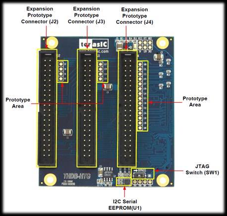
14 THDB-HTG Board This figure illustrates how the THDB-HTG board is connected to the DE2-115 board. Be sure to turn off the power whenever you connect or disconnect the THDB-HTG board!! 14

15 exp2_rsa.htm (1/2) DE2_115_User_manual.pdf 4.8 Usiing the Expansiion Header 15
")


16 exp2_rsa.htm (2/2) THDB-HTG_V1.0.3.pdf 1-6 Expansion Prototype Connectors 16

17 exp2_rsa.sdc Remember to modify the.sdc file. clock, i/o delay, etc. create_clock -period 1000 [get_ports clk] derive_clock_uncertainty set_input_delay 0 -clock clk [all_inputs] set_output_delay 0 -clock clk [all_outputs] 17
18 Can't place multiple pins? If you try to assign pins by yourself, this error message may occur. How to fix it? 18
19 1 2 19
20 1 20
21
22 1 22
23 ModelSim-Altera 23
24 Introduction to ModelSim (1/5) ModelSim is a simulation and verification tool for VHDL, Verilog, SystemVerilog, and mixed language designs. The following diagram shows the basic steps for simulating a design in ModelSim. Create a working library Compile design files Load and Run simulation Debug results 24
25 Introduction to ModelSim (2/5) Creating the Working Library In ModelSim, all designs are compiled into a library. You typically start a new simulation in ModelSim by creating a working library called "work," which is the default library name used by the compiler as the default destination for compiled design units. 25
26 Introduction to ModelSim (3/5) Compiling Your Design After creating the working library, you compile your design units into it. The ModelSim library format is compatible across all supported platforms. You can simulate your design on any platform without having to recompile your design. 26
27 Introduction to ModelSim (4/5) Loading the Simulator with Your Design and Running the Simulation With the design compiled, you load the simulator with your design by invoking the simulator on a top-level module (Verilog) or a configuration or entity/architecture pair (VHDL). 27
28 Introduction to ModelSim (5/5) Debugging Your Results If you don t get the results you expect, you can use ModelSim s robust debugging environment to track down the cause of the problem. 28
29 ModelSim-Altera Altera Quartus II software allows the user to launch Modelsim-Altera simulator from within the software using the Quartus II feature called NativeLink. It facilitates the process of simulation by providing an easy to use mechanism and precompiled libraries for simulation. 29
30 Setting up EDA Tool Options

31
32 Setting Up the Simulation
33

34
35 1 35
36 Before Simulation We should compile our design before simulation to generate a simulation snapshot. "Start Analysis & Elaboration" is enough, and it takes much less time than "Start Compilation". And then we can run the simulation. 36
37 Issues of Working Directory The working directory of ModelSim-Altera is under "(project directory)/simulation/modelsim", so be careful of setting the directory of input data in the testbench. 37
38
39

40 Congratulation! Be sure ModelSim-Altera has found the input data!! 40
41 If There are Something Wrong Your simulation takes a long time and seems it will not stop. The calculated result is incorrect. 41

42 If the Input Date are not Found It is a fake "PASS" 42


43 Change the Time Unit of the Timeline
 1")
44 Check the Waveform (1/2)

45 Check the Waveform (2/2) Zoom full Zoom Mode How to see the signals in the design? Just try it! 45
46 The End. Any question?
47 Reference 1. "DE2-115 User manual" by Terasic. 2. "THDB-HTG User Manual" by Terasic. 3. ModelSim Tutorial by Mentor Graphics Corporation. 4. "Getting Started with Quartus II Simulation Using the ModelSim-Altera Software User Guide" by Altera. 47
My First FPGA for Altera DE2-115 Board
 My First FPGA for Altera DE2-115 Board 數位電路實驗 TA: 吳柏辰 Author: Trumen Outline Complete Your Verilog Design Assign The Device Add a PLL Megafunction Assign the Pins Create a Default TimeQuest SDC File Compile
Timing Analyzer Quick-Start Tutorial
 Timing Analyzer Quick-Start Tutorial Intel Quartus Prime Pro Edition Updated for Intel Quartus Prime Design Suite: 17.1 Subscribe Send Feedback Latest document on the web: PDF HTML Contents Contents Timing
My First Nios II for Altera DE2-115 Board
 My First Nios II for Altera DE2-115 Board Digital Circuit Lab TA: Po-Chen Wu Outline Hardware Design Nios II IDE Build Flow Programming the CFI Flash 2 Hardware Design 3 Introduction This slides provides
Intel Quartus Prime Standard Edition Handbook Volume 3
 Intel Quartus Prime Standard Edition Handbook Volume 3 Verification Updated for Intel Quartus Prime Design Suite: 17.1 Subscribe Send Feedback Latest document on the web: PDF HTML Contents Contents 1.
Digital Design and Computer Architecture
 Digital Design and Computer Architecture Introduction Lab 4: Thunderbird Turn Signal In this lab, you will design a finite state machine in SystemVerilog to control the taillights of a 1965 Ford Thunderbird
2. Learn how to use Bus Functional Models (BFM) and write test cases for verifying your design.
 and write test cases for verifying your design.") Verifying your IP Objective The purpose of this tutorial is to guide a user through the simulation and verification framework available in quartus. By the end of this tutorial you will be able to : 1.
Verifying your IP Objective The purpose of this tutorial is to guide a user through the simulation and verification framework available in quartus. By the end of this tutorial you will be able to : 1.
UNIVERSITY OF CALIFORNIA, DAVIS Department of Electrical and Computer Engineering. EEC180A DIGITAL SYSTEMS I Winter 2015
 UNIVERSITY OF CALIFORNIA, DAVIS Department of Electrical and Computer Engineering EEC180A DIGITAL SYSTEMS I Winter 2015 LAB 1: Introduction to Quartus II Schematic Capture and ModelSim Simulation This
Cover TBD. intel Quartus prime Design software
 Cover TBD intel Quartus prime Design software Fastest Path to Your Design The Intel Quartus Prime software is revolutionary in performance and productivity for FPGA, CPLD, and SoC designs, providing a
CHAPTER 1 INTRODUCTION... 1 CHAPTER 2 ASSIGN THE DEVICE... 7 CHAPTER 3 DESIGN ENTRY CHAPTER 4 COMPILE AND VERIFY YOUR DESIGN...
 CONTENTS CHAPTER 1 INTRODUCTION... 1 1.1 DESIGN FLOW... 1 1.2 BEFORE YOU BEGIN... 2 1.3 WHAT YOU WILL LEARN... 6 CHAPTER 2 ASSIGN THE DEVICE... 7 2.1 ASSIGN THE DEVICE... 7 CHAPTER 3 DESIGN ENTRY... 11
Cover TBD. intel Quartus prime Design software
 Cover TBD intel Quartus prime Design software Fastest Path to Your Design The Intel Quartus Prime software is revolutionary in performance and productivity for FPGA, CPLD, and SoC designs, providing a
University of California, Davis Department of Electrical and Computer Engineering. Lab 1: Implementing Combinational Logic in the MAX10 FPGA
 1 University of California, Davis Department of Electrical and Computer Engineering EEC180B DIGITAL SYSTEMS II Winter Quarter 2018 Lab 1: Implementing Combinational Logic in the MAX10 FPGA Objective: This
Quick Tutorial for Quartus II & ModelSim Altera
 Quick Tutorial for Quartus II & ModelSim Altera By Ziqiang Patrick Huang Hudson 213c Ziqiang.huang@duke.edu Download & Installation For Windows or Linux users : Download Quartus II Web Edition v13.0 (ModelSim
Intel Quartus Prime Standard Edition Handbook Volume 3
 Intel Quartus Prime Standard Edition Handbook Volume 3 Verification Updated for Intel Quartus Prime Design Suite: 17.1 Subscribe Send Feedback Latest document on the web: PDF HTML Contents Contents 1 Simulating
Behavioral Modeling and Timing Constraints
 Introduction Behavioral modeling was introduced in Lab 1 as one of three widely used modeling styles. Additional capabilities with respect to testbenches were further introduced in Lab 4. However, there
Actel Libero TM Integrated Design Environment v2.3 Structural Schematic Flow Design Tutorial
 Actel Libero TM Integrated Design Environment v2.3 Structural Schematic Flow Design Tutorial 1 Table of Contents Design Flow in Libero TM IDE v2.3 Step 1 - Design Creation 3 Step 2 - Design Verification
CSEE W4840 Embedded System Design Lab 1
 CSEE W4840 Embedded System Design Lab 1 Stephen A. Edwards Due January 31, 2008 Abstract Learn to use the Altera Quartus development envrionment and the DE2 boards by implementing a small hardware design
Quartus II Tutorial. September 10, 2014 Quartus II Version 14.0
 Quartus II Tutorial September 10, 2014 Quartus II Version 14.0 This tutorial will walk you through the process of developing circuit designs within Quartus II, simulating with Modelsim, and downloading
ENSC 350 ModelSim Altera Tutorial
 ENSC 350 ModelSim Altera Tutorial This is a quick guide get you started with the ModelSim Altera simulator. ModelSim is only a functional verification tool so you will also have to use Quartus II to complete
Experiment VERI: FPGA Design with Verilog (Part 2) (webpage: /)
 (webpage: /)") Department of Electrical & Electronic Engineering 2 nd Year Laboratory Experiment VERI: FPGA Design with Verilog (Part 2) (webpage: www.ee.ic.ac.uk/pcheung/teaching/e2_experiment /) 1.0 Learning Outcomes
Department of Electrical & Electronic Engineering 2 nd Year Laboratory Experiment VERI: FPGA Design with Verilog (Part 2) (webpage: www.ee.ic.ac.uk/pcheung/teaching/e2_experiment /) 1.0 Learning Outcomes
Quartus II Version 14.0 Tutorial Created September 10, 2014; Last Updated January 9, 2017
 Quartus II Version 14.0 Tutorial Created September 10, 2014; Last Updated January 9, 2017 This tutorial will walk you through the process of developing circuit designs within Quartus II, simulating with
How to Customize the ModelSim Wave View in the Altera Quartus Simulation Flow
 How to Customize the ModelSim Wave View in the Altera Quartus Simulation Flow Cristian Sisterna Summary When ModelSim is automatically lunched from the Quartus environment, it just displays the top level
A STANDARDIZED PROCEDURE FOR CLOSING TIMING ON OpenHPSDR FPGA FIRMWARE DESIGNS
 A STANDARDIZED PROCEDURE FOR CLOSING TIMING ON OpenHPSDR FPGA FIRMWARE DESIGNS by Joe A. Martin, PhD, K5SO August 26, 2014 Introduction! 2 Running the Quartus II TimeQuest Utility! 3 The *.SDC file! 6
Intel Quartus Prime Pro Edition Handbook Volume 3
 Intel Quartus Prime Pro Edition Handbook Volume 3 Verification Updated for Intel Quartus Prime Design Suite: 17.1 Subscribe Send Feedback Latest document on the web: PDF HTML Contents Contents 1 Simulating
CS/EE 6710 Digital VLSI Design Tutorial on Cadence to Synopsys Interface (CSI)
") CS/EE 6710 Digital VLSI Design Tutorial on Cadence to Synopsys Interface (CSI) This tutorial walks you through the Cadence to Synopsys Interface (CSI). This interface lets you take a schematic from composer
CS/EE 6710 Digital VLSI Design Tutorial on Cadence to Synopsys Interface (CSI) This tutorial walks you through the Cadence to Synopsys Interface (CSI). This interface lets you take a schematic from composer
Circuit Design and Simulation with VHDL 2nd edition Volnei A. Pedroni MIT Press, 2010 Book web:
 Circuit Design and Simulation with VHDL 2nd edition Volnei A. Pedroni MIT Press, 2010 Book web: www.vhdl.us Appendix C Xilinx ISE Tutorial (ISE 11.1) This tutorial is based on ISE 11.1 WebPack (free at
CSEE W4840 Embedded System Design Lab 1
 CSEE W4840 Embedded System Design Lab 1 Stephen A. Edwards Due February 2, 2009 Abstract Learn to use the Altera Quartus development envrionment and the DE2 boards by implementing a small hardware design
Simulating Nios II Embedded Processor Designs
 Simulating Nios II Embedded Processor Designs May 2004, ver.1.0 Application Note 351 Introduction The increasing pressure to deliver robust products to market in a timely manner has amplified the importance
CSEE W4840 Embedded System Design Lab 1
 CSEE W4840 Embedded System Design Lab 1 Stephen A. Edwards Due February 3, 2011 Abstract Learn to use the Altera Quartus development envrionment and the DE2 boards by implementing a small hardware design
2. Mentor Graphics ModelSim and QuestaSim Support
 November 2012 QII53001-12.1.0 2. Mentor Graphics ModelSim and QuestaSim Support QII53001-12.1.0 This chapter provides specific guidelines for simulation of Quartus II designs with Mentor Graphics ModelSim-Altera,
SD Card Controller IP Specification
 SD Card Controller IP Specification Marek Czerski Friday 30 th August, 2013 1 List of Figures 1 SoC with SD Card IP core................................ 4 2 Wishbone SD Card Controller IP Core interface....................
CSE P567 - Winter 2010 Lab 1 Introduction to FGPA CAD Tools
 CSE P567 - Winter 2010 Lab 1 Introduction to FGPA CAD Tools This is a tutorial introduction to the process of designing circuits using a set of modern design tools. While the tools we will be using (Altera
Lecture 5: Aldec Active-HDL Simulator
 Lecture 5: Aldec Active-HDL Simulator 1. Objective The objective of this tutorial is to introduce you to Aldec s Active-HDL 9.1 Student Edition simulator by performing the following tasks on a 4-bit adder
Altera Technical Training Quartus II Software Design
 Altera Technical Training Quartus II Software Design Exercises Quartus II Software Design Series: Foundation 2 Quartus II Software Design Series: Foundation Exercises Exercise 1 3 Exercises Quartus II
DDR & DDR2 SDRAM Controller Compiler
 DDR & DDR2 SDRAM Controller Compiler march 2007, Compiler Version 7.0 Errata Sheet This document addresses known errata and documentation issues for the DDR and DDR2 SDRAM Controller Compiler version 7.0.
2.5G Reed-Solomon II MegaCore Function Reference Design
 2.5G Reed-Solomon II MegaCore Function Reference Design AN-642-1.0 Application Note The Altera 2.5G Reed-Solomon (RS) II MegaCore function reference design demonstrates a basic application of the Reed-Solomon
E85: Digital Design and Computer Engineering Lab 2: FPGA Tools and Combinatorial Logic Design
 E85: Digital Design and Computer Engineering Lab 2: FPGA Tools and Combinatorial Logic Design Objective The purpose of this lab is to learn to use Field Programmable Gate Array (FPGA) tools to simulate
SmartTime for Libero SoC v11.5
 SmartTime for Libero SoC v11.5 User s Guide NOTE: PDF files are intended to be viewed on the printed page; links and cross-references in this PDF file may point to external files and generate an error
DDR & DDR2 SDRAM Controller Compiler
 DDR & DDR2 SDRAM Controller Compiler August 2007, Compiler Version 7.1 Errata Sheet This document addresses known errata and documentation issues for the DDR and DDR2 SDRAM Controller Compiler version
Design Rules and Min Timing
 7 Design Rules and Min Timing Learning Objectives After completing this lab, you should be able to: Apply design rules and hold time constraints Fix design rule violations Fix hold time violations Lab
MicroBlaze Tutorial on EDK 10.1 using Sparatan III E Behavioural Simulation of MicroBlaze System
 MicroBlaze Tutorial on EDK 10.1 using Sparatan III E Behavioural Simulation of MicroBlaze System Ahmed Elhossini January 24, 2010 1 Introduction 1.1 Objectives This tutorial will demonstrate process of
TUTORIALS FOR MAX3000A CPLD DEVICES
 TUTORIALS FOR MAX3000A CPLD DEVICES WEL LAB 6-BIT-UP-DOWN-COUNTER CONTENTS: INTRODUCTION.. GETTING STARTED. DESIGN ENTRY. PIN ASSIGNMENT. PROGRAMMING CPLD DEVICE. REFERENCES. WEL LAB, IIT BOMBAY Page 2
Intel Quartus Prime Standard Edition User Guide
 Intel Quartus Prime Standard Edition User Guide Third-party Synthesis Updated for Intel Quartus Prime Design Suite: 18.1 Subscribe Latest document on the web: PDF HTML Contents Contents 1. Synopsys Synplify*
DDR & DDR2 SDRAM Controller Compiler
 DDR & DDR2 SDRAM Controller Compiler May 2006, Compiler Version 3.3.1 Errata Sheet This document addresses known errata and documentation issues for the DDR and DDR2 SDRAM Controller Compiler version 3.3.1.
Lab 6 : Introduction to Verilog
 Lab 6 : Introduction to Verilog Name: Sign the following statement: On my honor, as an Aggie, I have neither given nor received unauthorized aid on this academic work 1 Objective The main objective of
ELEC 4200 Lab#0 Tutorial
 1 ELEC 4200 Lab#0 Tutorial Objectives(1) In this Lab exercise, we will design and implement a 2-to-1 multiplexer (MUX), using Xilinx Vivado tools to create a VHDL model of the design, verify the model,
Xilinx ChipScope ICON/VIO/ILA Tutorial
 Xilinx ChipScope ICON/VIO/ILA Tutorial The Xilinx ChipScope tools package has several modules that you can add to your Verilog design to capture input and output directly from the FPGA hardware. These
EE 231 Fall Lab 1: Introduction to Verilog HDL and Altera IDE
 Lab 1: Introduction to Verilog HDL and Altera IDE Introduction In this lab you will design simple circuits by programming the Field-Programmable Gate Array (FPGA). At the end of the lab you should be able
TUTORIALS FOR MAX3000A CPLD DEVICES
 TUTORIALS FOR MAX3000A CPLD DEVICES WEL LAB BCD DECODER CONTENTS: INTRODUCTION.. GETTING STARTED. DESIGN ENTRY. PIN ASSIGNMENT. PROGRAMMING CPLD DEVICE. REFERENCES. WEL LAB, IIT BOMBAY Page 2 Introduction:
CHAPTER 1 INTRODUCTION Features About the KIT Getting Help... 7 CHAPTER 2 DE0-NANO BOARD ARCHITECTURE...
 1 CONTENTS CHAPTER 1 INTRODUCTION... 5 1.1 Features... 5 1.2 About the KIT... 7 1.3 Getting Help... 7 CHAPTER 2 DE0-NANO BOARD ARCHITECTURE... 8 2.1 Layout and Components... 8 2.2 Block Diagram of the
Turbo Encoder Co-processor Reference Design
 Turbo Encoder Co-processor Reference Design AN-317-1.2 Application Note Introduction The turbo encoder co-processor reference design is for implemention in an Stratix DSP development board that is connected
Verilog Simulation Mapping
 1 Motivation UNIVERSITY OF CALIFORNIA AT BERKELEY COLLEGE OF ENGINEERING DEPARTMENT OF ELECTRICAL ENGINEERING AND COMPUTER SCIENCE Lab 4 Verilog Simulation Mapping In this lab you will learn how to use
Quartus II Tutorial. September 10, 2014 Quartus II Version 14.0
 Quartus II Tutorial September 10, 2014 Quartus II Version 14.0 This tutorial will walk you through the process of developing circuit designs within Quartus II, simulating with Modelsim, and downloading
QuartusII.doc 25/02/2005 Page 1
 1 Start Icon... 2 1.1 The Quartus II Screen... 2 2 Project creation... 2 3 Schematic entry... 5 3.1 Create new drawing... 5 3.2 Symbol selection... 7 3.3 Placement of an AND gate... 8 3.4 Deleting a symbol...
SerialLite III Streaming IP Core Design Example User Guide for Intel Stratix 10 Devices
 SerialLite III Streaming IP Core Design Example User Guide for Intel Stratix 10 Devices Updated for Intel Quartus Prime Design Suite: 17.1 Stratix 10 ES Editions Subscribe Send Feedback Latest document
QUARTUS II Altera Corporation
 QUARTUS II Quartus II Design Flow Design Entry Timing Constraints Synthesis Placement and Routing Timing, Area, Power Optimization Timing and Power Analyzer Optimized Design 2 Can I still use a Processor?
King Fahd University of Petroleum and Minerals. Computer Engineering Department. COE 561 Digital Systems Design and Synthesis (Course Activity)
") King Fahd University of Petroleum and Minerals Computer Engineering Department COE 561 Digital Systems Design and Synthesis (Course Activity) Synthesis using Synopsys Design Compiler Tutorial The Synthesis
King Fahd University of Petroleum and Minerals Computer Engineering Department COE 561 Digital Systems Design and Synthesis (Course Activity) Synthesis using Synopsys Design Compiler Tutorial The Synthesis
Chapter 2: Hardware Design Flow Using Verilog in Quartus II
 Chapter 2: Hardware Design Flow Using Verilog in Quartus II 2.1 Introduction to Quartus II System Development Software This chapter is an introduction to the Quartus II software that will be used for analysis
Cell-Based Design Flow. TA : 吳廸優
 Cell-Based Design Flow TA : 吳廸優 dywu@viplab.cs.nctu.edu.tw 1 Outline Overview Design Flow Stage 1 RTL Development Synthesis Gate Level Simulation Design Flow Stage 2 Placement and Routing Post Layout Simulation
Designing RGMII Interface with FPGA and HardCopy Devices
 Designing RGMII Interface with FPGA and HardCopy Devices November 2007, ver. 1.0 Application Note 477 Introduction The Reduced Gigabit Media Independent Interface (RGMII) is an alternative to the IEEE
University of Florida EEL 3701 Dr. Eric M. Schwartz Madison Emas, TA Department of Electrical & Computer Engineering Revision 1 5-Jun-17
 Page 1/14 Example Problem Given the logic equation Y = A*/B + /C, implement this equation using a two input AND gate, a two input OR gate and two inverters under the Quartus environment. Upon completion
Mentor Graphics Solutions Enable Fast, Efficient Designs for Altera s FPGAs. Fall 2004
 Mentor Graphics Solutions Enable Fast, Efficient Designs for Altera s FPGAs Fall 2004 Agenda FPGA design challenges Mentor Graphics comprehensive FPGA design solutions Unique tools address the full range
NIOS CPU Based Embedded Computer System on Programmable Chip
 NIOS CPU Based Embedded Computer System on Programmable Chip 1 Lab Objectives EE8205: Embedded Computer Systems NIOS-II SoPC: PART-I This lab has been constructed to introduce the development of dedicated
Multiple Clocks and Timing Exceptions
 10 Multiple Clocks and Timing Exceptions Learning Objectives This lab is intended to give you a better understanding of how static timing analysis works and how timing exceptions are properly applied.
Verilog Simulation & Debugging Tools
 Verilog Simulation & Debugging Tools Digital Circuit Lab TA: Po-Chen Wu Outline Environment Setup NC-Verilog nlint nwave Verdi 2 Environment Setup 3 Login to the Linux Server Many EDA tools are provided
Terasic DE0 Field Programmable Gate Array (FPGA) Development Board
 Development Board") Lecture FPGA-01 DE0 FPGA Development Board and Quartus II 9.1 FPGA Design Software Terasic DE0 Field Programmable Gate Array (FPGA) Development Board 1 May 16, 2013 3 Layout and Components of DE0 May 16,
Lecture FPGA-01 DE0 FPGA Development Board and Quartus II 9.1 FPGA Design Software Terasic DE0 Field Programmable Gate Array (FPGA) Development Board 1 May 16, 2013 3 Layout and Components of DE0 May 16,
Getting a Quick Start 2
 2 Getting a Quick Start 2 This chapter walks you through the basic synthesis design flow (shown in Figure 2-1). You use the same basic flow for both design exploration and design implementation. The following
Tutorial on Quartus II Introduction Using Verilog Code
 Tutorial on Quartus II Introduction Using Verilog Code (Version 15) 1 Introduction This tutorial presents an introduction to the Quartus II CAD system. It gives a general overview of a typical CAD flow
Compiler User Guide. Intel Quartus Prime Pro Edition. Updated for Intel Quartus Prime Design Suite: Subscribe Send Feedback
 Compiler User Guide Intel Quartus Prime Pro Edition Updated for Intel Quartus Prime Design Suite: 18.0 Subscribe Send Feedback Latest document on the web: PDF HTML Contents Contents 1. Design Compilation...
Experiment 3 Introduction to Verilog Programming using Quartus II software Prepared by: Eng. Shatha Awawdeh, Eng.Eman Abu_Zaitoun
 Experiment 3 Introduction to Verilog Programming using Quartus II software Prepared by: Eng. Shatha Awawdeh, Eng.Eman Abu_Zaitoun Introduction: Verilog HDL is a hardware description language used to design
Specifying Timing Exceptions
 Specifying Timing Exceptions Learning Objectives This lab is intended to give you a better understanding of how static timing analysis works and how timing exceptions are applied properly. After completing
1.1 Features Block Diagram of the DE0-Nano Board Power-up the DE0-Nano Board Configuring the Cyclone IV FPGA...
 1 CONTENTS CHAPTER 1 INTRODUCTION... 5 1.1 Features...5 1.2 About the KIT...7 1.3 Getting Help...7 CHAPTER 2 DE0-NANO BOARD ARCHITECTURE... 8 2.1 Layout and Components...8 2.2 Block Diagram of the DE0-Nano
Managing Quartus II Projects
 1 QII52012 Subscribe The Quartus II software organizes and manages the elements of your design within a project. The project encapsulates information about your design hierarchy, libraries, constraints,
Introduction to the Qsys System Integration Tool
 Introduction to the Qsys System Integration Tool Course Description This course will teach you how to quickly build designs for Altera FPGAs using Altera s Qsys system-level integration tool. You will
Model-Based Design for Video/Image Processing Applications
 Model-Based Design for Video/Image Processing Applications The MathWorks Agenda Model-Based Design From MATLAB and Simulink to Altera FPGA Step-by-step design and implementation of edge detection algorithm
University of Twente. VHDL tutorial For internal use only. Faculty of Electrical Engineering, Mathematics and Computer Science. E.
 University of Twente Faculty of Electrical Engineering, Mathematics and Computer Science VHDL tutorial For internal use only E. Molenkamp January 2016 Contents 1 Introduction... 3 2 Simulation with ModelSim...
High Speed Memory Interfacing 800MHz DDR3 Memory Lab
 High Speed Memory Interfacing 800MHz DDR3 Memory Lab Software Requirements Overview 1) The Quartus II software version 11.1 2) Modelsim software version 11.1 This lab focuses on compiling and simulating
Contents. Appendix B HDL Entry Tutorial 2 Page 1 of 14
 Appendix B HDL Entry Tutorial 2 Page 1 of 14 Contents Appendix B HDL Entry Tutorial 2...2 B.1 Getting Started...2 B.1.1 Preparing a Folder for the Project...2 B.1.2 Starting Quartus II...2 B.1.3 Creating
Evaluation of the RTL Synthesis Tools for FPGA/PLD Design. M.Matveev. Rice University. August 10, 2001
 Evaluation of the RTL Synthesis Tools for FPGA/PLD Design M.Matveev Rice University August 10, 2001 Xilinx: Foundation ISE Design Entry: VHDL, Verilog, schematic, ABEL Synthesis: Xilinx XST, Synopsys FPGA
SerialLite III Streaming IP Core Design Example User Guide for Intel Arria 10 Devices
 IP Core Design Example User Guide for Intel Arria 10 Devices Updated for Intel Quartus Prime Design Suite: 17.1 Subscribe Send Feedback Latest document on the web: PDF HTML Contents Contents 1 Quick Start
A. Setting Up the Environment a. ~/ece394 % mkdir synopsys b.
 ECE 394 ASIC & FPGA Design Synopsys Design Compiler and Design Analyzer Tutorial A. Setting Up the Environment a. Create a new folder (i.e. synopsys) under your ece394 directory ~/ece394 % mkdir synopsys
Block-Based Design User Guide
 Block-Based Design User Guide Intel Quartus Prime Pro Edition Updated for Intel Quartus Prime Design Suite: 18.0 Subscribe Send Feedback Latest document on the web: PDF HTML Contents Contents 1. Block-Based
Intel High Level Synthesis Compiler
 Intel High Level Synthesis Compiler User Guide Updated for Intel Quartus Prime Design Suite: 18.0 Subscribe Send Feedback Latest document on the web: PDF HTML Contents Contents 1....3 2. Overview of the
CPEN 230L: Introduction to Digital Logic Laboratory Lab #6: Verilog and ModelSim
 CPEN 230L: Introduction to Digital Logic Laboratory Lab #6: Verilog and ModelSim Purpose Define logic expressions in Verilog using register transfer level (RTL) and structural models. Use Quartus II to
EE 4755 Digital Design Using Hardware Description Languages
 EE 4755 Digital Design Using Hardware Description Languages Basic Information URL: http://www.ece.lsu.edu/v Offered by: David M. Koppelman, Room 345 ERAD Building 578-5482. koppel@ece.lsu.edu, http://www.ece.lsu.edu/koppel/koppel.html
AccelDSP tutorial 2 (Matlab.m to HDL for Xilinx) Ronak Gandhi Syracuse University Fall
 Ronak Gandhi Syracuse University Fall") AccelDSP tutorial 2 (Matlab.m to HDL for Xilinx) Ronak Gandhi Syracuse University Fall 2009-10 AccelDSP Getting Started Tutorial Introduction This tutorial exercise will guide you through the process of
AccelDSP tutorial 2 (Matlab.m to HDL for Xilinx) Ronak Gandhi Syracuse University Fall 2009-10 AccelDSP Getting Started Tutorial Introduction This tutorial exercise will guide you through the process of
CME341 Assignment 4. module if\_else\_combinational\_logic( input [3:0] a, b, output reg [3:0] y ); * begin
![CME341 Assignment 4. module if\_else\_combinational\_logic( input [3:0] a, b, output reg [3:0] y ); * begin](/thumbs/82/87014840.jpg "CME341 Assignment 4. module if\_else\_combinational\_logic( input [3:0] a, b, output reg [3:0] y ); * begin") CME341 Assignment 4 1. The verilog description below is an example of how code can get butchered by an engineer with lazy debugging habits. The lazy debugger wanted to try something and yet be able to
CME341 Assignment 4 1. The verilog description below is an example of how code can get butchered by an engineer with lazy debugging habits. The lazy debugger wanted to try something and yet be able to
DC-Tcl Procedures. Learning Objectives. After completing this lab, you should be able to: Write generic DC-Tcl procedures. Lab Duration: 30 minutes
 w 14 Learning Objectives After completing this lab, you should be able to: Write generic DC-Tcl procedures Lab Duration: 30 minutes Lab 14-1 Synopsys 31833-000-S38 Flow Diagram of Lab Create and test myprocs.tcl
SignalTap II with Verilog Designs. 1 Introduction. For Quartus II 13.1
 SignalTap II with Verilog Designs For Quartus II 13.1 1 Introduction This tutorial explains how to use the SignalTap II feature within Altera s Quartus II software. The SignalTap II Embedded Logic Analyzer
2 nd Year Laboratory. Experiment: FPGA Design with Verilog. Department of Electrical & Electronic Engineering. Imperial College London.
 Department of Electrical & Electronic Engineering 2 nd Year Laboratory Experiment: FPGA Design with Verilog Objectives By the end of this experiment, you should know: How to design digital circuits using
ECE 3610 Microprocessing Systems Lab #1 Verilog Design of the TOC Using Quartus II
 ECE 3610 Microprocessing Systems Lab #1 Verilog Design of the TOC Using Quartus II This lab manual presents an introduction to the Quartus II Computer Aided Design (CAD) system. This manual gives step-by-step
Intel Quartus Prime Pro Edition Software and Device Support Release Notes
 Intel Quartus Prime Pro Edition Software and Device Support Release Notes Subscribe Send Feedback Latest document on the web: PDF HTML Contents Contents 1 Version 17.1... 3 1.1 New Features and Enhancements...3
Ethernet Switch. WAN Gateway. Figure 1: Switched LAN Example
 1 Introduction An Ethernet switch is used to interconnect a number of Ethernet LANs (Local Area Networks), forming a large Ethernet network. Different ports of the switch are connected to different LAN
SOPC LAB1. I. Introduction. II. Lab contents. 4-bit count up counter. Advanced VLSI Due Wednesday, 01/08/2003
 SOPC LAB1 I. Introduction The purpose of this lab is to familiarize you with all the items in the kit. This tutorial tells you how to develop FPGA system in Quartus II. You are ready to begin using the
Lab 1.5 (Warmup): Synthesis Workflow and SystemVerilog Register File Not Due
: Synthesis Workflow and SystemVerilog Register File Not Due") CMU 18-447: Introduction to Computer Architecture Lab 1.5 (Warmup): Synthesis Workflow and SystemVerilog Register File Not Due In this tutorial, you will take a quick tour of the tools we will use in this
CMU 18-447: Introduction to Computer Architecture Lab 1.5 (Warmup): Synthesis Workflow and SystemVerilog Register File Not Due In this tutorial, you will take a quick tour of the tools we will use in this
Lecture 1: Introduction Course arrangements Recap of basic digital design concepts EDA tool demonstration
 TKT-1426 Digital design for FPGA, 6cp Fall 2011 http://www.tkt.cs.tut.fi/kurssit/1426/ Tampere University of Technology Department of Computer Systems Waqar Hussain Lecture Contents Lecture 1: Introduction
Intel Quartus Prime Pro Edition User Guide
 Intel Quartus Prime Pro Edition User Guide Block-Based Design Updated for Intel Quartus Prime Design Suite: 18.1 Subscribe Latest document on the web: PDF HTML Contents Contents 1. Block-Based Design Flows...
Using ModelSim to Simulate Logic Circuits in VHDL Designs. 1 Introduction. For Quartus II 13.0
 Using ModelSim to Simulate Logic Circuits in VHDL Designs For Quartus II 13.0 1 Introduction This tutorial is a basic introduction to ModelSim, a Mentor Graphics simulation tool for logic circuits. We
QDRII SRAM Controller MegaCore Function User Guide
 QDRII SRAM Controller MegaCore Function User Guide 101 Innovation Drive San Jose, CA 95134 www.altera.com MegaCore Version: 9.1 Document Date: November 2009 Copyright 2009 Altera Corporation. All rights
Sidewinder Development Board rev 1.0
 33 Sidewinder Development Board rev 1.0 Features Altera MAX V CPLD 5M160ZT100C5 JTAG programmable USB programmable USB powered 12 On board LEDs 10 on board switches 3 RGB LEDs One 40 pin expansion headers
Introduction to the Altera SOPC Builder Using Verilog Design
 Introduction to the Altera SOPC Builder Using Verilog Design This tutorial presents an introduction to Altera s SOPC Builder software, which is used to implement a system that uses the Nios II processor