2001 by X Engineering Software Systems Corp., Apex, North Carolina 27502
|
|
|
- Lester West
- 5 years ago
- Views:
Transcription

1
2 2001 by X Engineering Software Systems Corp., Apex, North Carolina All rights reserved. No part of this text may be reproduced, in any form or by any means, without permission in writing from the publisher. The author and publisher of this text have used their best efforts in preparing this text. These efforts include the development, research, and testing of the theories and programs to determine their effectiveness. The author and publisher make no warranty of any kind, expressed or implied, with regard to these programs or the documentation contained in this text. The author and publisher shall not be liable in any event for incidental or consequential damages in connection with, or arising out of, the furnishing, performance, or use of these programs. XESS, XS40, and XS95 are trademarks of X Engineering Software Systems Corp. XILINX, Foundation, XC4000, and XC9500 are trademarks of XILINX Corporation. Other product and company names mentioned are trademarks or trade names of their respective companies. The software described in this text is furnished under a license agreement. The software may be used or copied under terms of the license agreement.
3 Table of Contents Table of Contents... i Introduction... 2 VHDL-Based Design... 5 In this chapter you will learn how to:... 5 Overall Design Flow... 5 Starting a Project... 8 Creating the VHDL Source Code Synthesizing a Netlist Running a Simulation Implementing the Design Downloading and Testing Retargeting the Circuit at an XC9500 CPLD by XESS Corp. i
4 0 Introduction There are numerous requests on Internet newgroups that go something like this: "I am new to using programmable logic like FPGAs and CPLDs. How do I start? Is there a tutorial and some cheap/free tools I can use to learn more?" Xilinx has a student edition of their Foundation 2.1I software so anyone can get a lowcost set of tools for designing with programmable logic. I have written this book to give you a gentle introduction to using the Foundation 2.1I software. (Other programmable logic manufacturers have released low-cost or free toolsets for their devices. Someone else will have to write a book for them.) This book tries to show you quickly how to use Foundation 2.1I to do the following: How to start a project and target it at a particular type of FPGA or CPLD. How to describe a logic circuit using VHDL, schematics, or both. How to simulate your circuit to test its functions. How to synthesize a netlist from your circuit. How to fit the netlist into an FPGA or CPLD. How to check the device utilization and timing. How to generate a bitstream for configuring the FPGA or CPLD. How to download the bitstream into the device. How to test the programmed device. I will use combinatorial and sequential logic design examples to illustrate the design flow. Along the way you will see how to use many of the tools bundled into XILINX Foundation 2.1I. I will not go into a great deal of explanation on the theory of operation of the example circuits or the internal circuitry of the programmable logic device, but I will provide references to the appropriate texts and application notes on these subjects. In short, this is just a tutorial to get you started using the XILINX Foundation tools. After you go through this book you can move on to more advanced topics. The basic concepts introduced in each chapter are shown below: Chapter 1 introduces the Foundation 2.1I software. In this chapter, you will use Foundation to describe a combinational circuit with VHDL, synthesize it, 2001 by XESS Corp. 2
5 simulate it, and then compile a configuration bitstream that you can download and test with an evaluation board. Chapter 2 shows you how to design and implement a combinational circuit using the schematic editor included in the Foundation software. Chapter 3 discusses how to do hierarchical and mixed-mode designs that include both schematics and VHDL. Chapter 4 describes the I/O characteristics of FPGAs and CPLDs and shows you how to specify them in your designs. Chapter 5 shows you how to design state machines using VHDL or the state machine editor included in the Foundation software. Chapter 6 discusses how to perform timing analysis of your combinational and sequential logic designs. Chapter 7 illustrates how to use the internal RAMs in a XILINX FPGA and how to interface an FPGA or CPLD to an external RAM chip. Chapter 8 describes a simple microcontroller and shows how to implement it in an FPGA and a CPLD. In addition to these chapters, there are two appendices in this text: Appendix A1 steps you through the installation of the Foundation software, its service pack updates, and its FlexLM license. Appendix A2 shows you how to configure and set-up your XS40 or XS95 Board so it can be used to run the design examples. You should read both appendices before beginning on Chapter 1. That ensures you have the software and hardware installed correctly and reduces the chance of encountering a problem while doing the examples. All the project files for each design example are provided on the CDROM. You should be able to re-create each design just from following the text, but you can use the project files in case you have problems or are in a hurry. Of equal importance, these working examples serve as a starting point for your own designs and explorations. After you complete this book will you be an expert in using programmable logic and the Foundation 2.1I tools? The answer is a definite NO. This text is just a starting point. After you complete this text you will be able to: Understand the basic structure of the XILINX XC9500 CPLDs and XC4000 FPGAs and be able to further your understanding by reading their respective datasheets. Understand the basic functions of the Foundation 2.1I software tools. Use Foundation to create, synthesize, simulate, and compile logic circuits for CPLDs and FPGAs by XESS Corp. 3
6 Analyze the performance of your circuit with respect to a given XILINX CPLD or FPGA. Download and test your circuit on an FPGA or CPLD evaluation board by XESS Corp. 4
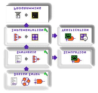
7 1 VHDL-Based Design In this chapter you will learn how to: Create a project with Foundation 2.1i. Enter VHDL code describing your logic circuit and check-and-correct any syntax errors. Pass the VHDL code to a synthesizer to generate a netlist for a particular FPGA or CPLD. Simulate the operations of the netlist to check the logical functions of your circuit. Transform the netlist into a configuration bitstream using the implementation tools. Download the bitstream into an FPGA or CPLD evaluation board. Test your circuit with the FPGA or CPLD evaluation board. Overall Design Flow Creating a logic circuit for a CPLD or FPGA usually consists of the following steps (depicted in Figure 1): 1. You enter a description of your logic circuit using a hardware description language (HDL) such as VHDL. 2. You use a logic synthesizer program to transform the HDL into a netlist. The netlist is just a description of the various logic gates in your design and how they are interconnected. 3. You test the functions of your circuit by loading the netlist into a simulator, applying input patterns (known as test vectors), and observing the simulated outputs. 5
8 Look at the datasheet and XAPP097 for more details about the XC4000XL FPGAs. The XC9500 datasheet and XAPP073 have more information about the internal structure of CPLDs. 4. You use implementation tools to map the logic gates and interconnections into the FPGA. The FPGA consists of an array of slices which can be further decomposed into configurable logic blocks (CLBs) that perform logic operations using a set of look-up tables (LUTs). The CLBs are interwoven with various local and global routing resources. The fitter places gates from your netlist in various CLBs in the slices and opens or closes switches in the routing resources to wire the gates together. (A similar process occurs when you use a CPLD except the slices are called configurable function blocks (CFBs), the CLBs are called macrocells, and the routing resources are called routing matrices.) 5. Once the implementation is complete, the state of the routing switches and CLBs (or macrocells) is extracted to create a bitstream where the ones and zeroes correspond to open or closed switches. 6. The bitstream is downloaded into a physical FPGA or CPLD chip (usually embedded in some larger system). The electronic switches in the device open or close in response to the binary bits in the bitstream. Upon completion of the downloading, the FPGA or CPLD will perform the operations specified by your HDL code. That's really all there is to it. XILINX Foundation 2.1i provides the HDL editor, logic synthesizer, simulator, implementation tools, and bitstream generator software. The GXSLOAD utility from XESS will download the bitstream into an XS40 FPGA Board or an XS95 CPLD Board. See page 372 of Digital Design Principles and Practices by John Wakerly for a detailed explanation of LED decoders. In the rest of this chapter we will follow the design flow of Figure 1 while designing a simple LED decoder circuit. The decoder will take a four-bit input that represents a hexadecimal number ( x0 0xF) and will output seven signals that drive a seven-segment LED display so it shows the corresponding hexadecimal digit (0, 1, 2, 3, 4, 5, 6, 7, 8, 9, A, b, C, d, E, F). 6
9 VHDL Source Code entity leddcd is port( d: in std_logic_vector(3 downto 0); s: out std_logic_vector(6 downto 0); ); end; Synthesize Netlist architecture leddcd_arch of leddcd is begin s <= " " when d="0000" else " " when d="0001" else " "; end leddcd_arch; CPLD Implement Simulate in0 in1 function block routing matrix routing resources macrocell FPGA out Generate Bitstream Bitstream slice XS40 or XS95 Board CLB Download and Test Figure 1: Steps in creating and testing an FPGA or CPLD-based design. 7

10 Starting a Project To begin the LED decoder project, double-click the 2.1i which will bring up the Project Manager window. start-up icon for Foundation 8


11 In the Getting Started dialog window, click on the Create a New Project radio button and then click on the OK button. The New Project window appears where you setup the project. First, you must specify the directory where the project design files will be stored. The Directory field is initialized with the default directory within the Foundation directory tree. It is OK to place your projects there, but in this book I will place all the examples in a separate directory called Prag21i. To do the same, begin by clicking on the Browse button. 9

12 Scroll down in the list of directories in the Browse for Folder window and highlight the Prag21i folder. Then click on OK. The path to the selected project folder will now appear in the Directory field. Next you must name your project. I placed the string dsgn1_1 in the Name field to indicate this is the first design of Chapter 1 of this book, but you can use any name you like. 10

13 Next, choose to create an HDL-based design rather than a schematic-based design by clicking on the HDL radio button. Once you do this, the fields for selecting the programmable device family will disappear from the bottom of the window. That s OK. We will select the target device for the LED decoder circuit when we run the synthesizer later on. This completes the initial setup for the LED decoder project, so click on the OK button. 11


14 Now the Project Manager window appears as shown below. You can execute operations using the menu items and buttons in the menu and toolbars across the top of the window. The results of these commands are reported in the Command History pane at the bottom of the window. Your current point within the process of creating your design is indicated within the Project Flow pane. And the various files that make up each iteration of your design are listed in the Project Hierarchy and Version pane. Menu and Tool Bars Project Flow Pane Project Hierarchy and Versions Pane Command History Pane 12
15 Creating the VHDL Source Code The first step is to enter your VHDL code for the LED decoder into a file. Start the HDL editor by clicking on the left-most icon of the Design Entry block in the Project Flow pane. 13


16 This brings up an HDL Editor window and a dialog box in which you can select how you want to enter your new code. If you are an experienced HDL coder, you will probably select the Create Empty option to start with an empty editor window where you can type-in your source directly. In this example, we will select the Use HDL Design Wizard option which will lead us through the creation of a code skeleton that we can modify to describe the LED decoder circuit. 14
.")
17 After clicking OK in the previous window, the Design Wizard window appears. Click Next> to move on. In the Design Wizard Language window, select the particular HDL you plan to use (VHDL in our case). Then click on Next>. 15
18 Type-in the name of the file in which you want to store the VHDL code. This does not have to be the same name as the entire project. I used leddcd for this example. After specifying the file name, click on Next>. The window for specifying the inputs and outputs of the LED decoder circuit now appears. Begin by clicking on the New button. 16
19 Next, type the name of the input port to the LED decoder. (I have named it d in this example.) The type of the port is selected by clicking one of the radio buttons in the Direction portion of the window. The Input button is selected by default so no action is needed in this case. As mentioned previously, the LED decoder takes a four-bit input so we need to set the width of the d input bus. Click three times on the upper-left button of the Bus field to set the d input to four bits as shown below. The d input bus will appear on the left-hand side of the design block and in the list of I/O ports. 17
20 Now that the description of the input port is completed, click on the New button to start describing the output port. Then click on the Output button to set the direction of the port. Type-in the name of the output port (s in this case) and then click on the upper-left Bus button six times. This sets the number of outputs to the seven required to drive a sevensegment LED. 18

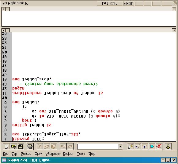
21 Now that the input and output ports have been described, click on the Finish button. A VHDL code skeleton for the LED decoder circuit now appears in the HDL Editor window. The skeleton is composed of the following parts: Lines 1 2: The standard IEEE library is linked in so our VHDL code can make use of the various functions and type declarations it contains. Lines 4 9: The ports through which the circuit inputs and outputs signals are defined in the entity section. Lines 11 14: The statements that describe the operations of the LED decoder circuit are placed in the architecture section. These statements will replace line
22 20
23 The skeleton code on line 13 is replaced with the VHDL code on lines shown in the window below. This code specifies the particular seven-bit value that will appear on the s outputs for each possible four-bit value that is driven into the d inputs. A high level on an output will illuminate the LED segment to which it is attached. (See Figure 2 for the correspondence between the s outputs and the individual segments that make up the LED digit.) 21

24 After entering the VHDL code, it s a good idea to see if there are any obvious errors. Do this by selecting the Synthesis Check Syntax menu item. 22

25 The syntax checker will parse the VHDL code and will return an error message in the bottom pane of the HDL Editor window informing you that there is an error on line 30. Click on the OK button to remove the pop-up error window. Line 30 was generated by the HDL Design Wizard, so it is unlikely that it has a syntax error. The actual error is at the end of line 29 where I have left off the terminating semicolon. 23

26 Once the semicolon is appended to line 29, the syntax checker is run again and the VHDL is judged to be free of syntax errors. Click on the OK button to remove the pop-up window. 24

27 Now that the code has passed the syntax checker, save it in the leddcd.vhd file using the File Save menu item. You can then exit from the editor. 25
28 We have a VHDL file that describes the LED decoder, but it isn t a part of our poject yet. We must add the file to our project using the Project Add Source files menu item. 26

29 The leddcd.vhd file will be seen in the Add Document window that appears. Highlight this file and then click on Open to add the file to the project. 27
30 The left-hand pane of the Project Manager window now shows the leddcd.vhd file that we added. The green checkmark by the file name indicates that the VHDL in the file is syntactically correct. The green checkmark in the Design Entry box in the right-hand pane denotes that this phase of the design flow is completed. 28
31 Synthesizing a Netlist Now that we have the VHDL description of the LED decoder completed, we can run the synthesizer on it to produce a netlist for the circuit. You can initiate this phase by clicking on the Synthesis box in the Design Flow pane of the Project Manager window. 29
32 We set the parameters that control the synthesis process in the Synthesis/Implementation settings window that appears. Of most importance is to select the target device for the LED decoder circuit. 30
33 We plan to test this design on an XS40-005XL Board that contains a XILINX XC4005XL FPGA chip in an 84-pin PLCC package. The XC4000XL FPGA family is already set in the Family field of the Target Device area of the window. So we only need to select the particular device in the family (XC4005XLPC84 in this case) from the drop-down list of the Device field. 31
34 We can also specify the speed grade of the device using the Speed field. The device in the XS40 Board is usually the slowest model, so select the 3 speed grade as shown below. There are many other synthesis options we could adjust by clicking on the SET button and selecting various options in the dialog windows that would appear. There is no need to do this for this simple example, but we will explore these options in more detail in following chapters. 32

35 Click on the Run button to start the synthesizer. A window with a progress bar will appear and show the various phases of the synthesis procedure. For this simple combinational circuit, the synthesis is completed in less than ten seconds on a fast PC. 33
36 The synthesizer shouldn t encounter any problems generating the netlist for the LED decoder circuit. Upon successful completion of the synthesis, you will see a green checkmark in the Synthesis box of the Design Flow pane in the Project Manager window. There are also two libraries that have been added to the Project Hierarchy pane: xc4000x and simprims. The xc4000x library contains circuit elements that we can add to logic circuits that are targeted to XC4000 FPGAs. The simprims library contains simulation primitives that are used when the Foundation simulator program is simulating a logic circuit targeted at any XILINX FPGA or CPLD. Right now we don t have to be concerned with what s in these libraries. 34
37 Running a Simulation Now that we have a netlist, we can use the simulator in Foundation to check the operation of the LED decoder. Click on the Simulation box in the Design Flow pane to activate the functional simulator. 35


38 The Logic Simulator window that appears contains a single Waveform Viewer 0 subwindow for viewing simulated waveforms of signals in the LED decoder circuit. Signal names are listed here Logic waveforms are displayed here 36
39 Now all we have to do is find a way to inject signals into the inputs of the LED decoder netlist and then observe the response of the outputs. We start by selecting the Signal Add Signals menu item. 37

40 The Component Selection for Waveform Viewer window appears with three panes. For our simple LED decoder, we are only interested in the left-hand Signals Selection pane. All the input and output ports for the LED decoder circuit are listed in this pane along with all the internal signals that connect the gates in the synthesized netlist. 38
41 For this example we are only concerned with the inputs and outputs of the LED decoder. Click on the top entry in the Signals Selection pane to highlight the set of four inputs to the LED decoder (D0, D1, D2, and D3). Then click on the Add button. 39

42 At this point a red checkmark should appear next to the input ports. This indicates that the four inputs to the LED decoder have been added to the Waveform Viewer 0 window. 40
43 Repeat the previous operation with the seven LED decoder outputs (S0, S1, S2, S3, S4, S5, and S6). Then click on the Close button to remove the Component Selection window. 41
44 Now you will see the input and output ports have been added to the Waveform Viewer window. The four input ports and seven output ports are grouped into buses as indicated by the B in the left-most column next to their signal names. Therefore, the logic levels on the four inputs and seven outputs will be grouped and displayed as hexadecimal values in the logic waveform pane of the Waveform Viewer window. 42

45 For this example it is more convenient to flatten the buses so we can observe the logic level on each individual input and output port. To do this, right-click on the output bus and select the Bus Flatten menu item in the cascading pop-up menues. 43

46 The individual signals in the output bus are now displayed in the Waveform Viewer window. 44
47 Next we repeat the bus flattening operation for the input bus. After doing this, we can see that the bus indicator in the left-most column of the Waveform Viewer window has been replaced with an i or o depending upon whether the flattened signal is an input or output, respectively. 45
48 Now that we have all the inputs and outputs displayed in the proper format, we need a way to stimulate the input ports with binary logic levels so we can observe the response on the output ports. Select the Signal Add Stimulators menu item to begin adding stimulators to the input ports. 46


49 Now the Stimulator Selection window appears and it has all the buttons and controls you would ever want to see. But we will only use a few for this example. In the middle of the window is a binary counter labeled Bc. This counter will increment once for each time step that the simulator executes during the simulation of the LED decoder. If we attach the four LED decoder inputs to the lower four bits of this counter, then we can force all possible input combinations into the decoder circuit over a span of sixteen simulation cycles. To begin attaching inputs to the binary counter bits, highlight the least-significant input port D0. Binary Counter 47
50 Once the D0 input port is highlighted, click on the least-significant bit of the binary counter. 48
51 Now we see that B0 has appeared in the column to the right of the D0 signal name, indicating that the least-significant input to the LED decoder has been connected to the least-significant bit of the stimulation counter. 49

52 We can repeat this operation to connect the succeeding three inputs of the LED decoder to the next three bits of the counter. Then click the Close button. 50


53 Now we are finally ready to test the LED decoder. To run the simulation, click on the Simulation Step button a few times. The right-hand pane of the Waveform Viewer window will display the binary counter values forced into the inputs and the resulting logic levels on the outputs of the LED decoder. The simulation covers a time interval of 50 ns. Forced inputs from binary counter Simulated output levels 51

54 The waveforms may be a bit squeezed to view easily, so you can click the Zoom In button to expand the time scale. Now we can check the output levels for each input combination to see if they match the input-output pairs specified in the VHDL code. For example, when all the inputs are at logic level 0, then all the outputs are at a high logic level except for S3. This agrees with the behavior specified on line 14 of the leddcd.vhd file. You can check the response to the remaining fifteen input combinations in a similar fashion. 52


55 We can exit the simulator now that we have verified the operation of the LED decoder, but it is wise to save the state of the simulator in case we have to come back and do more tests later. That way we don t have to go through all the effort of adding the input and output signals and attaching stimulators again. Begin this task by selecting the File Save Simulation State menu item. In the Save Simulation window that appears, type leddcd.des into the File name field and click on OK. The current state of the simulator will be saved into this file in the project folder. You can restore the simulator to this saved state by clicking File Load simulation State in the Logic Simulator window and selecting the leddcd.des file. 53
56 Finally we can select File Exit to terminate this simulation session. 54
57 Implementing the Design Now that the simulation has given us some confidence that our circuit is performing as an LED decoder, we want to transform the netlist into a bitstream that we can run on a real XC4005XL FPGA in an XS40 evaluation board. The FPGA has some of its pins connected to the parallel port of the PC attached to the XS40 board. We can use the PC to drive logic levels through the parallel port and onto the pins of the FPGA where they will serve as inputs to the LED decoder in the FPGA. The FPGA also has seven pins connected to a seven-segment LED digit. The outputs from the LED decoder should be connected to these pins so we can easily see if the circuit operates correctly. We will create a user-constraints file that will tell the Foundation implementation tools which LED decoder inputs or output should be assigned to a particular physical pin of the FPGA. Parallel Port Connector D0 D1 D2 D3 D4 D5 D6 D XC4005XL FPGA S0 S1 S2 S3 S4 S5 S6 S5 S2 S6 S3 S0 S4 S1 Figure 2: Connection of the parallel port and LED digit to the pins of the FPGA on the XS40 Board. 55
58 To begin creating the user constraints, select the Project Add Source File(s) menu item in the Project Manager window. 56

59 Foundation 2.1i automatically created a user-constraints file called dsgn1_1.ucf when we started this project. Select this file in the Add Document window and click on Open. 57

60 The dsgn1_1.ucf user-constraints file is now added to the project hierarchy. We will place our pin assignments for the LED decoder in this file. Right-click on the dsgn1_1.ucf label in the Project Hierarchy pane and select Edit in the pop-up menu. 58

61 The design1_1.ucf file contents now appear in the Report Browser window. Foundation placed a large amount of information about writing constraints in the file when it was created. You can use Edit Select All and Edit Delete to remove all these comments from the file, or you can just add your own constraints to the file. 59
62 The window below shows the pin assignment constraints used when the LED decoder circuit is targeted to an XS40 Board. The net keyword is followed by the name of one of the inputs or outputs of the circuit. The Foundation synthesizer places <> around the index of each element in an input or output bus in the netlist, so signal d0 (for example) must be referred to as d<0> in the user constraints file. The signal name is followed by a location constraint indicated by the loc keyword followed by the particular pin the signal is assigned to. For example, input signal d0 is assigned to pin 44 on the 84-pin PLCC package of the XC4005XL FPGA on the XS40 Board. 60
63 After entering all the constraints, click on File Save and File Exit to save the new pin assignment constraints and close the file. 61
64 Now we can start the implementation tools by clicking on the Implementation block in the Design Flow pane. 62
65 We are again presented with the Synthesis/Implementation setting window just as we were when we activated the synthesizer in a previous phase of the design flow. But now we can only set the options and control files that affect the implementation tools all the synthesis settings and the target device selector are locked. This makes sense since the synthesizer generated a netlist based upon the characteristics of the XC4000 FPGA, so we cannot decide to implement that netlist on a different type of programmable device which may not have the same features. We need to inform the implementation tools about the user constraints file with the pin assignments for the LED decoder. Click on the SET button in the Physical Implementation settings area to do this. 63
66 The Settings window lets us specify several types of control files. Guide files are used if we want the implementation tools to use what they learned in a previous implementation of this circuit to guide the current implementation process. Similarly, floorplanning files are created by the designer to give the implementation tools hints about where they should place the netlist components and wires within the FPGA or CPLD programmable arrays. Guide and floorplanning files can significantly reduce the time required to complete the implementation phase. We haven t run the implementation tools on the LED decoder yet, and we haven t created a floorplan for the circuit so neither of these options is of interest to us. 64

67 But we do have a user constraints file, so click on the Use Constraints file from: field and select Custom. The Custom window will display the dsgn1_1.ucf file by default, so all we need to do is click on OK to enable the use of this control file. 65

68 Now click OK to finalize the settings for the implementation tools. Then click on Run to start the implementation tools. 66

69 The Flow Engine window appears that depicts the progress through the five phases of the FPGA implementation process. Running appears below the currently active phase while Completed appears for each successfully completed step. Status and error messages generated during each implementation step scroll through the lower section of the window. The purpose of each phase is as follows: Translate: The synthesized netlist format and the user constraints are converted into an internal database format. Map: The logic gates in the netlist are grouped to take advantage of the resources in the FPGA s CLBs. Place&Route: The mapped logic gates are placed in specific locations within the FPGA s array of CLBs and the connections between the gates are routed through the FPGA s wiring resources. Timing (Sim): The propagation delays through the CLBs and routing are computed and stored for use during a timing simulation. (This phase is optional and can be turned off if you don t want to do timing simulations.) Configure: The bitstream that will configure an FPGA with the placed-and-routed circuit is generated. 67

70 Once all five phases of the implementation process have completed, click on OK in the status pop-up window. A successful implementation is indicated by the green checkmark in the Implementation box in the Design Flow pane. We can check how much of the FPGA is used by the LED decoder circuit by selecting the Implementation View Report Files menu item or clicking on the report browser toolbar button as shown below. 68

71 The Report Browser window lists the reports generated by each phase of the implementation process. We can double-click the Place & Route Report icon to get a view of the statistics on the usage of FPGA resources. Scrolling downward through the place-and-route report brings us to the device utilization summary. The LED decoder has four inputs and seven outputs, so it uses eleven of the 61 input/output blocks (IOBs) of the XC4005XL FPGA. The design is completely combinational so its uses none of the FPGA s flip-flops and latches. It does use four of the 392 CLBs in the FPGA. Each CLB contains two four-input lookup tables (LUTs) and one three-input LUT that perform all the combinational logic duties. The LED decoder requires seven LUTs to generate its seven outputs, and these seven LUTs are packed into four CLBs. Overall, we see the LED decoder circuit doesn t use much of the FPGA at all. 69


72 We should also check to see if our pin assignment constraints were obeyed. Doubleclick the Pad Report icon to inspect the actual pin assignments. The input and output names are listed in the pad report file along with the pin number to which they were assigned during the implementation phase. We can see that the actual pin assignments match the assignments we placed in the dsgn1_1.ucf user constraints file. 70

73 Downloading and Testing We have successfully synthesized, simulated, and implemented the LED decoder, so now we can test it in an actual FPGA. First we should locate the actual LED decoder bitstream. It can be found in the C:\Prag21\dsgn1_1\xproj\ver1\rev1 folder in the dsgn1_1.bit file. Now apply power to the XS40 Board, connect it to the parallel port of your PC, and double-click the GXSLOAD icon to start the process of loading the LED decoder bitstream into the XC4005XL FPGA. 71


74 Then just drag-and-drop the dsgn1_1.bit file from the rev1 window into the gxsload window. Once the bitstream file is dropped in the gxsload window, a progress bar will appear to show the percentage of the bitstream transmitted to the FPGA. The download should take less than ten seconds, after which a pop-up window will appear to indicate the XS40 FPGA Board is programmed. Click on OK to remove the pop-up window. 72
75 Now we need to drive the inputs of the LED decoder and observe its response on the LED digit of the XS40 Board. Double-click the GXSPORT icon to start up the utility that can drive the FPGA inputs through the PC parallel port. The gxsport window has eight buttons that correspond to the eight parallel port data pins. The current level on each data pin is reflected in the binary digit displayed within each button. Clicking a data button toggles the level, but the new output is not driven onto the parallel port pin until the Strobe button is pressed. We can drive test vectors into the LED decoder circuit by pressing buttons D0, D1, D2, and D3 to set the desired pattern and then clicking Strobe. But there is a faster way than typing in all sixteen input vectors. Just check the Count box to make the eight-bit value represented by D7 D0 increment every time Strobe is pressed. Then just click Strobe sixteen times. You should see the LED display the next hexadecimal digit after each click. 73
76 Retargeting the Circuit at an XC9500 CPLD At this point we have synthesized, simulated, implemented, downloaded, and tested the LED decoder on an XC4005XL FPGA. Now we will retarget the LED decoder at an XC95108 CPLD device. We will create a new version of the project to hold the modified design. To start, select the Project Create Version menu item. 74
77 Note that the Version name field has automatically been set to ver2 In the Create Version window that appears. Set the fields in the Target Device area to the values needed for the XS95 Board as shown below. Next, click on the Run button to activate the synthesizer. The synthesizer will create a new netlist the takes into account the specific features of the XC9500 CPLD architecture. 75


 and implemented.")

78 After the netlist synthesis is complete, the Project Manager window shows a green checkmark in the Synthesis block of the Design Flow pane. The version label in the Design Flow pane has also been changed to ver2. We can view more details about the different versions of the LED decoder project by clicking on the Versions tab in the Project Hierarchy pane. We see that ver1 is targeted to an XC4005XL FPGA and has been successfully synthesized (both functional and optimized netlists are present) and implemented. The ver2 version, however, is targeted at an XC95108 CPLD and has only been synthesized to this point. No implementation phase has been performed yet. (That accounts for the yellow question mark in the Implementation block of the Design Flow pane.) We can activate a version by clicking on its name in the Versions tab. The ver2 version is currently active, so we will leave it that way. Name of active version 76
79 As compared to the XS40 Board, the CPLD on the XS95 Board has different pins connected to the parallel port and LED digit. Therefore, we need to change the pin assignment constraints in the dsgn1_1.ucf file. Click on the Files tab in the Project Hierarchy pane and then double-click the dsgn1_1.ucf file name to edit the user constraints file. 77

80 Edit the pin assignments for the XS95 Board as follows. Then save the file and exit. Parallel Port Connector D0 D1 D2 D3 D4 D5 D6 D XC95108 CPLD S0 S1 S2 S3 S4 S5 S6 S5 S2 S6 S3 S0 S4 S1 Figure 3: Connection of the parallel port and LED digit to the pins of the CPLD on the XS95 Board. 78
81 Now start the implementation tools that will map the netlist to the XC95108 CPLD. 79
82 The Synthesis/Implementation setting window will appear. Press the SET button so we can tell the implementation tools where to find the updated user constraint file. In the Settings window, the drop-down list for the Use Constraints file from: field contains a few more entries than it did last time. The first two entries refer to constraint files for the previous version targeted at the XC4005XL FPGA, so they are not suitable for this version. Select the Custom entry. 80

83 Click on the Browse button in the Custom window that appears. Then move to the top level of the project where the modified user constraints file is found. Highlight the user constraints file and click on Open. 81

84 The Custom window now reflects the name of the user constraints file. Click on OK. Then click on OK in the Settings window. 82
85 Now that the user constraints file for the XS95 Board has been specified, click on Run to start the implementation tools. 83

86 The Flow Engine window appears, but only four steps are required for a CPLD implementation versus the five steps used in an FPGA implementation. (The Fit step does the same things for a CPLD that the Map and Place&Route steps do for an FPGA.) The implementation phase should complete without incident. 84

87 Now that the implementation is completed (note the green checkmark in the Implementation box), we can check the CPLD utilization and pin assignments with the report browser. For CPLDs, the device utilization summary and the pin assignments are both recorded in the Fitting Report. Double-click the icon to view this file. The summary of the CPLD resources that are used by the LED decoder is placed at the top of the file. The circuit uses eleven I/O pins of the 69 present on the CPLD. Seven 85

88 macrocells are used to hold the combinational logic for the LED decoder s outputs. As with the FPGA, the LED decoder does not consume much of the CPLD resources. 86


89 The pin assignments are found further down in the file. As expected, the implementation tools assigned the inputs and outputs to the same pins that we specified in the user constraints file. Pin number column 87

90 We need to do a little more processing on the bitstream output by the implementation tools before we can download them to an XC9500 CPLD. Click on the Programming box in the Design Flow pane to begin this step. 88


91 The JTAG Programmer window will appear displaying a single XC95108 device. We need to translate the bitstream into the SVF format that is compatible with the GXSLOAD utility. Select Output Create SVF File to store the translated bitstream into a file. 89

92 In the SVF Options window, select the Through Test-Logic-Reset radio button. This will insure that the downloading circuitry of the XC9500 CPLD is properly initialized before the bitstream enters the device. Then click on OK. The Create a New SVF File window will appear next. By default, the SVF file will be stored in the folder for this verison and revision of the project in a file called dsgn1_1.svf. Just click on Save to accept these defaults. 90
93 Once the SVF file specified, it is time to generate the translated bitstream. Since the bitstream is going to be programmed into the CPLD, select the Operations Program item from the menu list. 91

 None of the other options are applicable to this example so they should be left unchecked.")
94 The Options window will appear with a set of actions we can add to the programming bitstream. The Erase Before Programming option should be checked to force the CPLD to erase its internal Flash storage before the new bitstream is loaded. (Failure to erase the storage can lead to errors if the CPLD was previously programmed with a different bitstream.) None of the other options are applicable to this example so they should be left unchecked. (Definitely do not check the Write Protect box or you will be unable to load new bitstreams into the CPLD in the future.) Click on OK after setting the options as shown below. An Operation Status window appears to show you the progress as the SVF file is generated. Click on OK after all operations are complete. 92


95 Now that the SVF file with the translated bitstream has been created, we can exit the JTAG Programmer window. Upon exiting the JTAG Programmer window, you will be asked if you want to save any changes. This is rarely necessary so click on No. (This will not affect the SVF file that was already created.) 93


96 Now we have to go find the SVF file with the bitstream. It will be stored in the folder for reversion rev1 of version ver2 of the dsgn1_1 project as shown below. With the XS95 Board connected to a power supply and the PC parallel port, just dragand-drop the dsgn1_1.svf file over to the gxsload window. 94


97 It will take a minute or so for the bitstream to download into the XC95108 CPLD on the XS95 Board. (Most of this time is used to erase the nonvolatile Flash memory in the CPLD that stores the bitstream.) Once the XS95 Board is programmed, we can test it in exactly the same way we tested the LED decoder circuit with the XS40 Board. The results should be the identical. 95
Using XILINX WebPACK Software to Create CPLD Designs
 Introduction to WebPACK Using XILINX WebPACK Software to Create CPLD Designs RELEASE DATE: 10/24/1999 All XS-prefix product designations are trademarks of XESS Corp. All XC-prefix product designations
Introduction to WebPACK 3.1. Using XILINX WebPACK Software to Create CPLD Designs
 Introduction to WebPACK 3.1 Using XILINX WebPACK Software to Create CPLD Designs RELEASE DATE: 8/28/2000 All XS-prefix product designations are trademarks of XESS Corp. All XC-prefix product designations
Introduction to WebPACK 4.1 for CPLDs. Using Xilinx WebPACK Software to Create CPLD Designs for the XS95 Board
 Introduction to WebPACK 4.1 for CPLDs Using Xilinx WebPACK Software to Create CPLD Designs for the XS95 Board Release date: 10/29/2001 All XS-prefix product designations are trademarks of XESS Corp. All
Introduction to WebPACK 6.3. Using Xilinx WebPACK Software to Create FPGA Designs for the XSA Board
 Introduction to WebPACK 6.3 Using Xilinx WebPACK Software to Create FPGA Designs for the XSA Board Release date: 1/1/2005 2005 by XESS Corp. All XS-prefix product designations are trademarks of XESS Corp.
Introduction to WebPACK 4.1 for FPGAs. Using Xilinx WebPACK Software to Create FPGA Designs for the XSA Board
 Introduction to WebPACK 4.1 for FPGAs Using Xilinx WebPACK Software to Create FPGA Designs for the XSA Board Release date: 10/29/2001 All XS-prefix product designations are trademarks of XESS Corp. All
Introduction to WebPACK 8.1. Using Xilinx WebPACK Software to Create FPGA Designs for the XSA Board
 Introduction to WebPACK 8.1 Using Xilinx WebPACK Software to Create FPGA Designs for the XSA Board Release date: 5/16/2005 2006 by XESS Corp. All XS-prefix product designations are trademarks of XESS
Introduction to WebPACK 6.1. Using Xilinx WebPACK Software to Create FPGA Designs for the XSA Board
 Introduction to WebPACK 6.1 Using Xilinx WebPACK Software to Create FPGA Designs for the XSA Board Release date: 10/30/2003 All XS-prefix product designations are trademarks of XESS Corp. All XC-prefix
Introduction to WebPACK 5.2 for FPGAs. Using Xilinx WebPACK Software to Create FPGA Designs for the XSB-300E Board
 Introduction to WebPACK 5.2 for FPGAs Using Xilinx WebPACK Software to Create FPGA Designs for the XSB-300E Board Release date: 10/27/2003 All XS-prefix product designations are trademarks of XESS Corp.
Digital Circuit Design Using Xilinx ISE Tools
 Digital Circuit Design Using Xilinx ISE Tools Poras T. Balsara and Prashant Vallur Table of Contents 1. Introduction 2. Programmable logic devices: FPGA and CPLD 3. Creating a new project in Xilinx Foundation
TLL5000 Electronic System Design Base Module
 TLL5000 Electronic System Design Base Module The Learning Labs, Inc. Copyright 2007 Manual Revision 2007.12.28 1 Copyright 2007 The Learning Labs, Inc. Copyright Notice The Learning Labs, Inc. ( TLL )
TLL5000 Electronic System Design Base Module. Getting Started Guide, Ver 3.4
 TLL5000 Electronic System Design Base Module Getting Started Guide, Ver 3.4 COPYRIGHT NOTICE The Learning Labs, Inc. ( TLL ) All rights reserved, 2008 Reproduction in any form without permission is prohibited.
UNIVERSITY OF CALIFORNIA, DAVIS Department of Electrical and Computer Engineering. EEC180A DIGITAL SYSTEMS I Winter 2015
 UNIVERSITY OF CALIFORNIA, DAVIS Department of Electrical and Computer Engineering EEC180A DIGITAL SYSTEMS I Winter 2015 LAB 1: Introduction to Quartus II Schematic Capture and ModelSim Simulation This
Getting Started with Xilinx Design Tools and the XS 40 Prototyping Platform-- a User s Guide *
 Getting Started with Xilinx Design Tools and the XS 40 Prototyping Platform-- a User s Guide * B. Earl Wells Sin Ming Loo by Electrical and Computer Engineering Department University of Alabama in Huntsville
Tutorial: Working with Verilog and the Xilinx FPGA in ISE 9.2i
 Tutorial: Working with Verilog and the Xilinx FPGA in ISE 9.2i This tutorial will show you how to: Use Verilog to specify a design Simulate that Verilog design Define pin constraints for the FPGA (.ucf
Digital Electronics & Computer Engineering (E85)
") Digital Electronics & Computer Engineering (E85) Lab 4: Thunderbird Turn Signal Introduction In this lab, you will design a finite state machine to control the taillights of a 1965 Ford Thunderbird 1 and
Digital Electronics & Computer Engineering (E85) Lab 4: Thunderbird Turn Signal Introduction In this lab, you will design a finite state machine to control the taillights of a 1965 Ford Thunderbird 1 and
Verilog Design Entry, Synthesis, and Behavioral Simulation
 ------------------------------------------------------------- PURPOSE - This lab will present a brief overview of a typical design flow and then will start to walk you through some typical tasks and familiarize
Physics 623. FPGA I Construction of a Synchronous Counter Aug. 4, 2008
 Physics 623 FPGA I onstruction of a Synchronous ounter Aug. 4, 2008 1 The Goal of This Experiment You will design a small digital circuit, download the design to a Field Programmable Gate Array (FPGA)
Tutorial on Quartus II Introduction Using Verilog Code
 Tutorial on Quartus II Introduction Using Verilog Code (Version 15) 1 Introduction This tutorial presents an introduction to the Quartus II CAD system. It gives a general overview of a typical CAD flow
Xilinx Project Navigator Reference Guide
 31 July 2003 Author: David M. Sendek Xilinx Project Navigator Reference Guide Background: This guide provides you with step-by-step procedures in using the Xilinx Project Navigator to perform the following:
Programmable Logic Design Techniques I
 PHY 440 Lab14: Programmable Logic Design Techniques I The design of digital circuits is a multi-step process. It starts with specifications describing what the circuit must do. Defining what a circuit
Xilinx Tutorial Basic Walk-through
 Introduction to Digital Logic Design with FPGA s: Digital logic circuits form the basis of all digital electronic devices. FPGAs (Field Programmable Gate Array) are large programmable digital electronic
Contents. Appendix B HDL Entry Tutorial 2 Page 1 of 14
 Appendix B HDL Entry Tutorial 2 Page 1 of 14 Contents Appendix B HDL Entry Tutorial 2...2 B.1 Getting Started...2 B.1.1 Preparing a Folder for the Project...2 B.1.2 Starting Quartus II...2 B.1.3 Creating
MANUAL XILINX ISE PROJECT NAVIGATOR
 Hochschule für Angewandte Wissenschaften Hamburg University of Applied Sciences Department of Electrical Engineering and Computer Sciences MANUAL XILINX ISE PROJECT NAVIGATOR AND MODELSIM Design Flow for
and 32 bit for 32 bit. If you don t pay attention to this, there will be unexpected behavior in the ISE software and thing may not work properly!
 This tutorial will show you how to: Part I: Set up a new project in ISE 14.7 Part II: Implement a function using Schematics Part III: Simulate the schematic circuit using ISim Part IV: Constraint, Synthesize,
Tutorial on Quartus II Introduction Using Schematic Designs
 Tutorial on Quartus II Introduction Using Schematic Designs (Version 15) 1 Introduction This tutorial presents an introduction to the Quartus II CAD system. It gives a general overview of a typical CAD
Engineering 1630 Fall Simulating XC9572XL s on the ENGN1630 CPLD-II Board
 Engineering 1630 Fall 2016 Simulating XC9572XL s on the ENGN1630 CPLD-II Board You will use the Aldec Active-HDL software for the required timing simulation of the XC9572XL CPLD programmable logic chips
University of Florida EEL 3701 Dr. Eric M. Schwartz Department of Electrical & Computer Engineering Revision 0 12-Jun-16
 Page 1/14 Quartus Tutorial with Basic Graphical Gate Entry and Simulation Example Problem Given the logic equation Y = A*/B + /C, implement this equation using a two input AND gate, a two input OR gate
Tutorial 2 Implementing Circuits in Altera Devices
 Appendix C Tutorial 2 Implementing Circuits in Altera Devices In this tutorial we describe how to use the physical design tools in Quartus II. In addition to the modules used in Tutorial 1, the following
EE183 LAB TUTORIAL. Introduction. Projects. Design Entry
 EE183 LAB TUTORIAL Introduction You will be using several CAD tools to implement your designs in EE183. The purpose of this lab tutorial is to introduce you to the tools that you will be using, Xilinx
Logic Implementation on a Xilinx FPGA using VHDL WWU Linux platform assumed. rev 10/25/16
 1 Logic Implementation on a Xilinx FPGA using VHDL WWU Linux platform assumed. rev 10/25/16 The following is a general outline of steps (i.e. design flow) used to implement a digital system described with
ENGN 1630: CPLD Simulation Fall ENGN 1630 Fall Simulating XC9572XLs on the ENGN1630 CPLD-II Board Using Xilinx ISim
 ENGN 1630 Fall 2018 Simulating XC9572XLs on the ENGN1630 CPLD-II Board Using Xilinx ISim You will use the Xilinx ISim simulation software for the required timing simulation of the XC9572XL CPLD programmable
RTL Design and IP Generation Tutorial. PlanAhead Design Tool
 RTL Design and IP Generation Tutorial PlanAhead Design Tool Notice of Disclaimer The information disclosed to you hereunder (the "Materials") is provided solely for the selection and use of Xilinx products.
Actel Libero TM Integrated Design Environment v2.3 Structural Schematic Flow Design Tutorial
 Actel Libero TM Integrated Design Environment v2.3 Structural Schematic Flow Design Tutorial 1 Table of Contents Design Flow in Libero TM IDE v2.3 Step 1 - Design Creation 3 Step 2 - Design Verification
Getting Started with Xilinx WebPack 13.1
 Getting Started with Xilinx WebPack 13.1 B. Ackland June 2011 (Adapted from S. Tewksbury notes WebPack 7.1) This tutorial is designed to help you to become familiar with the operation of the WebPack software
Quartus II Introduction Using Verilog Design
 Quartus II Introduction Using Verilog Design This tutorial presents an introduction to the Quartus R II CAD system. It gives a general overview of a typical CAD flow for designing circuits that are implemented
Active-HDL. Getting Started
 Active-HDL Getting Started Active-HDL is an integrated environment designed for development of VHDL designs. The core of the system is a VHDL simulator. Along with debugging and design entry tools, it
The board is powered by the USB connection, so to turn it on or off you plug it in or unplug it, respectively.
 Lab 1 You may work in pairs or individually on this lab Lab Objectives Learn about the equipment we will be using and how to handle it safely. Learn the basics of using Xilinx ISE to develop hardware designs
CCE 3202 Advanced Digital System Design
 CCE 3202 Advanced Digital System Design Lab Exercise #2 Introduction You will use Xilinx Webpack v9.1 to allow the synthesis and creation of VHDLbased designs. This lab will outline the steps necessary
ELEC 4200 Lab#0 Tutorial
 1 ELEC 4200 Lab#0 Tutorial Objectives(1) In this Lab exercise, we will design and implement a 2-to-1 multiplexer (MUX), using Xilinx Vivado tools to create a VHDL model of the design, verify the model,
ECSE-323 Digital System Design. Lab #1 Using the Altera Quartus II Software Fall 2008
 1 ECSE-323 Digital System Design Lab #1 Using the Altera Quartus II Software Fall 2008 2 Introduction. In this lab you will learn the basics of the Altera Quartus II FPGA design software through following
Tutorial: Working with the Xilinx tools 14.4
 Tutorial: Working with the Xilinx tools 14.4 This tutorial will show you how to: Part I: Set up a new project in ISE Part II: Implement a function using Schematics Part III: Implement a function using
Physics 623. Programmable Gate Array Experiment Nov. 30, 2006
 Physics 623 Programmable Gate Array Experiment Nov. 30, 2006 1 The Goal of This Experiment You will design a small digital circuit, download the design to a Field Programmable Gate Array (FPGA) I, and
Chapter 2 Getting Hands on Altera Quartus II Software
 Chapter 2 Getting Hands on Altera Quartus II Software Contents 2.1 Installation of Software... 20 2.2 Setting Up of License... 21 2.3 Creation of First Embedded System Project... 22 2.4 Project Building
Logic Implementation on a Xilinx FPGA using VHDL WWU Linux platform assumed. rev 11/01/17
 1 Logic Implementation on a Xilinx FPGA using VHDL WWU Linux platform assumed. rev 11/01/17 The following is a general outline of steps (i.e. design flow) used to implement a digital system described with
Quartus II Introduction Using Schematic Design
 Quartus II Introduction Using Schematic Design This tutorial presents an introduction to the Quartus R II CAD system. It gives a general overview of a typical CAD flow for designing circuits that are implemented
Chip Design with FPGA Design Tools
 Chip Design with FPGA Design Tools Intern: Supervisor: Antoine Vazquez Janusz Zalewski Florida Gulf Coast University Fort Myers, FL 33928 V1.9, August 28 th. Page 1 1. Introduction FPGA is abbreviation
CCE 3202 Advanced Digital System Design
 CCE 3202 Advanced Digital System Design Lab Exercise #2 This lab exercise will show you how to create, synthesize, and test a 3-bit ripple counter. A ripple counter is simply a circuit that outputs the
2 nd Year Laboratory. Experiment: FPGA Design with Verilog. Department of Electrical & Electronic Engineering. Imperial College London.
 Department of Electrical & Electronic Engineering 2 nd Year Laboratory Experiment: FPGA Design with Verilog Objectives By the end of this experiment, you should know: How to design digital circuits using
Quick Front-to-Back Overview Tutorial
 Quick Front-to-Back Overview Tutorial PlanAhead Design Tool This tutorial document was last validated using the following software version: ISE Design Suite 14.5 If using a later software version, there
Programmable Logic Devices
 Programmable Logic Devices INTRODUCTION A programmable logic device or PLD is an electronic component used to build reconfigurable digital circuits. Unlike a logic gate, which has a fixed function, a PLD
Xilinx Schematic Entry Tutorial
 Overview Xilinx Schematic Entry Tutorial Xilinx ISE Schematic Entry & Modelsim Simulation What is circuit simulation and why is it important? Complex designs, short design cycle Simultaneous system design
University of Florida EEL 3701 Dr. Eric M. Schwartz Madison Emas, TA Department of Electrical & Computer Engineering Revision 1 5-Jun-17
 Page 1/14 Example Problem Given the logic equation Y = A*/B + /C, implement this equation using a two input AND gate, a two input OR gate and two inverters under the Quartus environment. Upon completion
Tutorial: ISE 12.2 and the Spartan3e Board v August 2010
 Tutorial: ISE 12.2 and the Spartan3e Board v12.2.1 August 2010 This tutorial will show you how to: Use a combination of schematics and Verilog to specify a design Simulate that design Define pin constraints
CPLD Experiment 4. XOR and XNOR Gates with Applications
 CPLD Experiment 4 XOR and XNOR Gates with Applications Based on Xilinx ISE Design Suit 10.1 Department of Electrical & Computer Engineering Florida International University Objectives Materials Examining
Lab 1 Modular Design and Testbench Simulation ENGIN 341 Advanced Digital Design University of Massachusetts Boston
 Lab 1 Modular Design and Testbench Simulation ENGIN 341 Advanced Digital Design University of Massachusetts Boston Introduction This lab introduces the concept of modular design by guiding you through
Designing Your Own Soft Modules
 4 Objectives Learn how to create circuit schematics with OrCAD Learn how to export a circuit from OrCAD as an EDIF netlist. Learn how to import an EDIF netlist into the FastChip library as a new soft module.
Xilinx ISE/WebPack: Introduction to Schematic Capture and Simulation
 Xilinx ISE/WebPack: Introduction to Schematic Capture and Simulation Revision: February 7, 2003 Overview This document is intended to assist new entry-level users of the Xilinx ISE/WebPack software. It
Revision: February 27, E Main Suite D Pullman, WA (509) Voice and Fax
 Voice and Fax") Xilinx ISE WebPACK Schematic Capture Tutorial Revision: February 27, 2010 215 E Main Suite D Pullman, WA 99163 (509) 334 6306 Voice and Fax Overview This tutorial provides instruction for using the Xilinx
Xilinx ISE WebPACK Schematic Capture Tutorial Revision: February 27, 2010 215 E Main Suite D Pullman, WA 99163 (509) 334 6306 Voice and Fax Overview This tutorial provides instruction for using the Xilinx
Altera Quartus II Tutorial ECE 552
 Altera Quartus II Tutorial ECE 552 Quartus II by Altera is a PLD Design Software which is suitable for high-density Field-Programmable Gate Array (FPGA) designs, low-cost FPGA designs, and Complex Programmable
Quartus II Introduction Using Verilog Designs. 1 Introduction. For Quartus II 12.0
 Quartus II Introduction Using Verilog Designs For Quartus II 12.0 1 Introduction This tutorial presents an introduction to the Quartus II CAD system. It gives a general overview of a typical CAD flow for
EMT1250 LABORATORY EXPERIMENT. EXPERIMENT # 6: Quartus II Tutorial and Practice. Name: Date:
 EXPERIMENT # 6: Quartus II Tutorial and Practice Name: Date: Equipment/Parts Needed: Quartus II R Web Edition V9.1 SP2 software by Altera Corporation USB drive to save your files Objective: Learn how to
ISE Simulator (ISim) In-Depth Tutorial. UG682 (v 13.1) March 1, 2011
 In-Depth Tutorial. UG682 (v 13.1) March 1, 2011") ISE Simulator (ISim) In-Depth Tutorial Xilinx is disclosing this user guide, manual, release note, and/or specification (the "Documentation") to you solely for use in the development of designs to operate
ISE Simulator (ISim) In-Depth Tutorial Xilinx is disclosing this user guide, manual, release note, and/or specification (the "Documentation") to you solely for use in the development of designs to operate
Laboratory of Digital Circuits Design: Design, Implementation and Simulation of Digital Circuits Using Programmable Devices
 Internet Engineering Dr. Jarosław Sugier Laboratory of Digital Circuits Design: Design, Implementation and Simulation of Digital Circuits Using Programmable Devices This document presents software packages
Chapter 3. HDL Editor. Introduction. Figure 3-1. HDL Editor Welcome Screen. Introduction 3-1
 Introduction 3-1 Chapter 3 HDL Editor Introduction The HDL editor is used for entering and editing designs expressed by ABEL and VHDL programs statements. The HDL editor is invoked by clicking on the HDL
Tutorial for Altera DE1 and Quartus II
 Tutorial for Altera DE1 and Quartus II Qin-Zhong Ye December, 2013 This tutorial teaches you the basic steps to use Quartus II version 13.0 to program Altera s FPGA, Cyclone II EP2C20 on the Development
Introduction to Computer Engineering (E114)
") Introduction to Computer Engineering (E114) Lab 1: Full Adder Introduction In this lab you will design a simple digital circuit called a full adder. You will then use logic gates to draw a schematic for
Introduction to Computer Engineering (E114) Lab 1: Full Adder Introduction In this lab you will design a simple digital circuit called a full adder. You will then use logic gates to draw a schematic for
Using ModelSim to Simulate Logic Circuits in VHDL Designs. 1 Introduction. For Quartus II 13.0
 Using ModelSim to Simulate Logic Circuits in VHDL Designs For Quartus II 13.0 1 Introduction This tutorial is a basic introduction to ModelSim, a Mentor Graphics simulation tool for logic circuits. We
Introduction. About this tutorial. How to use this tutorial
 Basic Entry & not About this tutorial This tutorial consists of an introduction to creating simple circuits on an FPGA using a variety of methods. There are two ways to create the circuit: using or by
Field Programmable Gate Array
 Field Programmable Gate Array System Arch 27 (Fire Tom Wada) What is FPGA? System Arch 27 (Fire Tom Wada) 2 FPGA Programmable (= reconfigurable) Digital System Component Basic components Combinational
Vivado Tutorial. Introduction. Objectives. Procedure
 Lab Workbook Introduction This tutorial guides you through the design flow using Xilinx Vivado software to create a simple digital circuit using VHDL. A typical design flow consists of creating model(s),
Programming Xilinx SPARTAN 3 Board (Simulation through Implementation)
") Programming Xilinx SPARTAN 3 Board (Simulation through Implementation) September 2008 Prepared by: Oluwayomi Adamo Class: Project IV University of North Texas FPGA Physical Description 4 1. VGA (HD-15)
Programming Xilinx SPARTAN 3 Board (Simulation through Implementation) September 2008 Prepared by: Oluwayomi Adamo Class: Project IV University of North Texas FPGA Physical Description 4 1. VGA (HD-15)
Adding the ILA Core to an Existing Design Lab
 Adding the ILA Core to an Existing Introduction This lab consists of adding a ChipScope Pro software ILA core with the Core Inserter tool and debugging a nonfunctioning design. The files for this lab are
FPGA Design Tutorial
 ECE 554 Digital Engineering Laboratory FPGA Design Tutorial Version 5.0 Fall 2006 Updated Tutorial: Jake Adriaens Original Tutorial: Matt King, Surin Kittitornkun and Charles R. Kime Table of Contents
CECS LAB 1 Introduction to Xilinx EDA Tools
 NAME: DUE DATE: STUDENT ID: POSSIBLE POINTS: 10 COURSE DATE & TIME: OBJECTIVE: To familiarize ourselves with the Xilinx Electronic Design Aid (EDA) Tools. We will simulate a simple 4-to-1 Multiplexor using
NIOS CPU Based Embedded Computer System on Programmable Chip
 1 Objectives NIOS CPU Based Embedded Computer System on Programmable Chip EE8205: Embedded Computer Systems This lab has been constructed to introduce the development of dedicated embedded system based
Experimental 1-Bit Adder for the XS40 Board
 'i Table 3.8 Truth-table for a 2-bit adder with carry input and output. i Input 1 InputO Carry Input Sum Output Carry Output I 0 0 0 0 0 0 0 1 1 1 0 0 1 0 1 0 0 l' 1 0 1 1 ( 0 0 1 0 1 0 1 0 1 1 1 0 I 0.
PlanAhead Software Tutorial
 PlanAhead Software Tutorial RTL Design and IP Generation The information disclosed to you hereunder (the Information ) is provided AS-IS with no warranty of any kind, express or implied. Xilinx does not
Logic Design With Soft Modules
 You can download your design once the bind process completes. As always, make sure your CSoC Board is attached to the 9V DC power supply and it is connected to the parallel port of your PC with the downloading
EE 367 Logic Design Lab #1 Introduction to Xilinx ISE and the ML40X Eval Board Date: 1/21/09 Due: 1/28/09
 EE 367 Logic Design Lab #1 Introduction to Xilinx ISE and the ML40X Eval Board Date: 1/21/09 Due: 1/28/09 Lab Description Today s lab will introduce you to the Xilinx Integrated Software Environment (ISE)
ECE 3610 Microprocessing Systems Lab #1 Verilog Design of the TOC Using Quartus II
 ECE 3610 Microprocessing Systems Lab #1 Verilog Design of the TOC Using Quartus II This lab manual presents an introduction to the Quartus II Computer Aided Design (CAD) system. This manual gives step-by-step
Building Combinatorial Circuit Using Behavioral Modeling Lab
 Building Combinatorial Circuit Using Behavioral Modeling Lab Overview: In this lab you will learn how to model a combinatorial circuit using behavioral modeling style of Verilog HDL. You will model a combinatorial
Using Synplify Pro, ISE and ModelSim
 Using Synplify Pro, ISE and ModelSim VLSI Systems on Chip ET4 351 Rene van Leuken Huib Lincklaen Arriëns Rev. 1.2 The EDA programs that will be used are: For RTL synthesis: Synplicity Synplify Pro For
Quick Tutorial for Quartus II & ModelSim Altera
 Quick Tutorial for Quartus II & ModelSim Altera By Ziqiang Patrick Huang Hudson 213c Ziqiang.huang@duke.edu Download & Installation For Windows or Linux users : Download Quartus II Web Edition v13.0 (ModelSim
SCHEMATIC DESIGN IN QUARTUS
 SCHEMATIC DESIGN IN QUARTUS Consider the design of a three-bit prime number detector. Figure 1 shows the block diagram and truth table. The inputs are binary signals A, B, and C while the output is binary
Xilinx ISE8.1 and Spartan-3 Tutorial (Prepared by Kahraman Akdemir based on Professor Duckworth's Tutorials updated September 2006)
") Xilinx ISE8.1 and Spartan-3 Tutorial (Prepared by Kahraman Akdemir based on Professor Duckworth's Tutorials updated September 2006) 1 Part1) Starting a new project Simple 3-to-8 Decoder Start the Xilinx
Xilinx ISE8.1 and Spartan-3 Tutorial (Prepared by Kahraman Akdemir based on Professor Duckworth's Tutorials updated September 2006) 1 Part1) Starting a new project Simple 3-to-8 Decoder Start the Xilinx
Parallel Cable III Emulator for the XSB-300E Board
 Parallel Cable III Emulator for the XSB-300E Board October 4, 2003 (Version 1.0) Application Note by D. Vanden Bout Summary This application note shows how to configure the XC9572XL CPLD on the XSB-300E
PlanAhead Software Tutorial
 RTL Design and IP Generation with CORE Generator UG 675 (v 12.1) May 3, 2010 Xilinx is disclosing this Document and Intellectual Property (hereinafter the Design ) to you for use in the development of
Tutorial 3. Appendix D. D.1 Design Using Verilog Code. The Ripple-Carry Adder Code. Functional Simulation
 Appendix D Tutorial 3 This tutorial introduces more advanced capabilities of the Quartus II system. We show how Verilog code is organized and compiled and illustrate how multibit signals are represented
QUARTUS II Altera Corporation
 QUARTUS II Quartus II Design Flow Design Entry Timing Constraints Synthesis Placement and Routing Timing, Area, Power Optimization Timing and Power Analyzer Optimized Design 2 Can I still use a Processor?
Tutorial on FPGA Design Flow based on Aldec Active HDL. Ver 1.5
 Tutorial on FPGA Design Flow based on Aldec Active HDL Ver 1.5 1 Prepared by Ekawat (Ice) Homsirikamol, Marcin Rogawski, Jeremy Kelly, John Pham, and Dr. Kris Gaj This tutorial assumes that you have basic
Parallel Cable III Emulator for the XSV Board
 Parallel Cable III Emulator for the XSV Board June 1, 2002 (Version 1.1) Application Note by D. Vanden Bout Summary This application note shows how to configure the XC95108 CPLD on the XSV Board so its
Lab 1: Introduction to Verilog HDL and the Xilinx ISE
 EE 231-1 - Fall 2016 Lab 1: Introduction to Verilog HDL and the Xilinx ISE Introduction In this lab simple circuits will be designed by programming the field-programmable gate array (FPGA). At the end
Tutorial on FPGA Design Flow based on Xilinx ISE WebPack and ModelSim. ver. 2.0
 Tutorial on FPGA Design Flow based on Xilinx ISE WebPack and ModelSim ver. 2.0 Updated: Fall 2013 1 Preparing the Input: Download examples associated with this tutorial posted at http://ece.gmu.edu/tutorials-and-lab-manuals
FPGA Introductory Tutorial: Part 1
 FPGA Introductory Tutorial: Part 1 This tutorial is designed to assist in learning the basics of the Altera Quartus II v9.0 software. Part 1 of the tutorial will cover the basics of creating a Project,
SOPC LAB1. I. Introduction. II. Lab contents. 4-bit count up counter. Advanced VLSI Due Wednesday, 01/08/2003
 SOPC LAB1 I. Introduction The purpose of this lab is to familiarize you with all the items in the kit. This tutorial tells you how to develop FPGA system in Quartus II. You are ready to begin using the
FPGA for Complex System Implementation. National Chiao Tung University Chun-Jen Tsai 04/14/2011
 FPGA for Complex System Implementation National Chiao Tung University Chun-Jen Tsai 04/14/2011 About FPGA FPGA was invented by Ross Freeman in 1989 SRAM-based FPGA properties Standard parts Allowing multi-level
Banks, Jasmine Elizabeth (2011) The Spartan 3E Tutorial 1 : Introduction to FPGA Programming, Version 1.0. [Tutorial Programme]
![Banks, Jasmine Elizabeth (2011) The Spartan 3E Tutorial 1 : Introduction to FPGA Programming, Version 1.0. [Tutorial Programme]](/thumbs/75/72381729.jpg "Banks, Jasmine Elizabeth (2011) The Spartan 3E Tutorial 1 : Introduction to FPGA Programming, Version 1.0. [Tutorial Programme]") QUT Digital Repository: http://eprints.qut.edu.au/ This is the author version published as: This is the accepted version of this article. To be published as : This is the author s version published as:
QUT Digital Repository: http://eprints.qut.edu.au/ This is the author version published as: This is the accepted version of this article. To be published as : This is the author s version published as:
Vivado Design Suite User Guide
 Vivado Design Suite User Guide Design Flows Overview Notice of Disclaimer The information disclosed to you hereunder (the Materials ) is provided solely for the selection and use of Xilinx products. To
PlanAhead Software Tutorial
 UG 677 (v 12.1.1) May 11, 2010 Xilinx is disclosing this Document and Intellectual Property (hereinafter the Design ) to you for use in thedevelopment of designs to operate on, or interface with Xilinx
Xilinx ChipScope ICON/VIO/ILA Tutorial
 Xilinx ChipScope ICON/VIO/ILA Tutorial The Xilinx ChipScope tools package has several modules that you can add to your Verilog design to capture input and output directly from the FPGA hardware. These