TM57ME15B& ME15CG DATA SHEET
|
|
|
- Oswin Pierce
- 5 years ago
- Views:
Transcription

1 TM57ME15B& ME15CG DATA SHEET Rev 0.91 tenx reserves the right to change or discontinue the manual and online documentation to this product herein to improve reliability, function or design without further notice. tenx does not assume any liability arising out of the application or use of any product or circuit described herein; neither does it convey any license under its patent rights nor the rights of others. tenx products are not designed, intended, or authorized for use in life support appliances, devices, or systems. If Buyer purchases or uses tenx products for any such unintended or unauthorized application, Buyer shall indemnify and hold tenx and its officers, employees, subsidiaries, affiliates and distributors harmless against all claims, cost, damages, and expenses, and reasonable attorney fees arising out of, directly or indirectly, any claim of personal injury or death associated with such unintended or unauthorized use even if such claim alleges that tenx was negligent regarding the design or manufacture of the part.
2 AMENDMENT HISTORY Version Date Description 0.90 Apr, 2018 New Release.TM57ME15 is revised to TM57ME15B 1. Add high sink description (p5, p7) 2. Modify ordering information (p74) 0.91 Aug, 原 ME15B 增加一型號 ME15CG, 合併為一份 DS- TM57ME15B_ME15CG_E 2. 加入 ME15CG 差異表 (p7) 3. 移除 ME15 pahsed out 敘述 (p7) 4. 加入 ME15CG ordering information(p74) DS-TM57ME15B_ME15CG_E 2 Rev 0.91, 2018/08/14
3 CONTENTS AMENDMENT HISTORY... 2 CONTENTS... 3 FEATURES... 5 BLOCK DIAGRAM... 8 PIN ASSIGNMENT... 9 PIN DESCRIPTIONS PIN SUMMARY FUNCTIONAL DESCRIPTION CPU Core Program ROM (PROM) System Configuration Register (SYSCFG) RAM Addressing Mode Programming Counter (PC) and Stack Reset Power on Reset Low Voltage Reset External Pin Reset Watchdog Timer Reset Clock Circuitry and Operation Mode System Clock Dual System Clock Modes Transition Improve the Stability of FIRC/FXRC Low Dropout Regulator Interrupt I/O Port PA0-6, PB PA Watchdog Timer (WDT) / Wakeup Timer (WKT) Timer Timer PWM0: 8 bits PWM MEMORY MAP INSTRUCTION SET ELECTRICAL CHARACTERISTICS DS-TM57ME15B_ME15CG_E 3 Rev 0.91, 2018/08/14
4 1. Absolute Maximum Ratings DC Characteristics Clock Timing Reset Timing Characteristics LVR Circuit Characteristics Characteristic Graphs PACKAGING INFORMATION DS-TM57ME15B_ME15CG_E 4 Rev 0.91, 2018/08/14
5 FEATURES ROM: 1K x 14 bits MTP (Multi Time Programmable ROM) 1. RAM: 48 x 8 bits 2. STACK: 5 Levels 3. I/O ports: Maximum 12 programmable I/O pins Open-Drain Output CMOS Push-Pull Output Schmitt Trigger Input with pull-up resistor option PA0~PA7, PB0~PB3 pin level change wake-up Up to 11 pins with high sink current (40mA). 4. System Oscillation Sources (Fsys) : Fast-clock - FIRC (Fast Internal RC) : 16 MHz - FXRC (Fast External R) : 1~16MHz - FXT (Fast Crystal) : 1~16 MHz Slow-clock - SIRC (Slow Internal RC) : SXT (Slow Crystal) : Hz 5. System Clock Prescaler: System Oscillation Sources can be divided by 1/2/4/16 as System Clock (Fsys) 6. Dual System Clock: (FIRC or FXRC) + SIRC FXT + SIRC FIRC + SXT 7. Power Saving Operation Mode FAST Mode: Slow-clock can be disabled or enabled, Fast-clock keeps CPU running SLOW Mode: Fast-clock can be disabled or enabled, Slow-clock keeps CPU running IDLE Mode: Fast-clock and CPU stop. Slow-clock, Timer2, or Wake-up Timer keep running STOP Mode: All clocks stop, Timer2 and Wake-up Timer stop 8. Two Independent Timers Timer0 (TM0) - 8-bit timer divided by 1~256 pre-scale option, Reload/Interrupt/Stop function Timer2 (T2) - 15-bit Timer2 with 4 interrupt time period options - IDLE mode wake-up timer or used as one simple 15-bit time base DS-TM57ME15B_ME15CG_E 5 Rev 0.91, 2018/08/14
6 - Clock sources: Slow-clock (SIRC/SXT), Fsys/ Interrupts Three External Interrupt pins - Two pins are falling edge triggered interrupt & wake-up functions - One pin is rising or falling edge triggered interrupt & wake-up functions Timer0/Timer2/WKT (wake-up) Interrupts PWM0 Interrupt LVD Interrupt 10. Wake-up Timer (WKT) Clocked by built-in RC oscillator with 4 adjustable interrupt times - 16 ms/32 ms/64 ms/ ms/24 ms/48 ms/ Watchdog Timer (WDT) Clocked by built-in RC oscillator with 4 adjustable reset times ms/256 ms/1024 ms/ ms/192 ms/768 ms/1536 Watchdog timer can be disabled/enabled in STOP mode 12. One PWM PWM0: - 8 bits, duty-adjustable, period-adjustable controlled PWM - PWM0 clock source: Fast-clock or FIRC 16 MHz, with 1~64 pre-scales 13. Reset Sources Power On Reset/Watchdog Reset/Low Voltage Reset/External Pin Reset 14. Low Voltage Reset (LVR) Options and Low Voltage Detection (LVD): If LVR is disabled, power on V CC must exceed the lowest LVR level C) 3-Level Low Voltage Reset: 2.0V/2.3V/2.9V 1-Level Low Voltage Detection: 2.3V 15. Operating Voltage: Fsys=16 MHz, 2.4~5.5V, power on V CC must exceed the selected LVR level Fsys=8 MHz, 1.8~5.5V, power on V CC must exceed the selected LVR level Fsys=4 MHz, 1.6~5.5V, power on V CC must exceed the selected LVR level Fsys=1 MHz, 1.5~5.5V, power on V CC must exceed the selected LVR level Fsys=SIRC, 1.3~5.5V, power on V CC must exceed the selected LVR level Fsys=32768 Hz, 1.3~5.5V, power on V CC must exceed the selected LVR level 16. Operating Temperature Range: -40 C to + 85 C DS-TM57ME15B_ME15CG_E 6 Rev 0.91, 2018/08/14
7 17. Table Read Instruction: 14-bit ROM data lookup table 18. Instruction set: 39 Instructions 19. Instruction Execution Time 2 system clocks (Fsys) per instruction except branch 20. Programming connectivity support 5-wire (ICP) or 8-wire program 21. Package Types: SOP-8/SOP-14/DIP-8/DIP Supported EV board on ICE EV board: EV8217 Comparison between EV8217, TM57ME15B, TM57ME15CG and TM57PE15A TM57ME15 had phased out on Nov. 2017, user can use TM57ME15B to replace TM57ME15. EV8217 TM57ME15B TM57ME15CG TM57PE15A EV board - EV8217 EV8217 EV2786B Fast-clock FXT/FXRC/FIRC FXT/FXRC/FIRC FXT/FXRC/FIRC FXT/FIRC Slow-clock SXT/SIRC SXT/SIRC SXT/SIRC SXT/XRC/SIRC FIRC + SIRC FIRC/FXRC + SIRC FIRC/FXRC + SIRC FIRC/FXRC + SIRC FIRC + XRC Dual system clock FIRC + SXT FIRC + SXT FIRC + SXT FIRC + SXT FXT + SIRC FXT + SIRC FXT + SIRC FXT + SIRC LVR/LVD levels LVR 2.0V/2.3V/2.9V LVD 2.3V LVR 2.0V/2.3V/2.9V LVD 2.3V LVR 2.0V/2.3V/2.9V LVD 2.3V LVR 1.7V/2.3V/3.1V LVD 2.5V/3.3V WDT/WKT WDT 128~2048ms WDT 128~2048ms WDT 128~2048ms WDT 12~96ms WKT 16~128ms WKT 16~128ms WKT 16~128ms WKT 12~96ms Pin wakeup PA7~0, PB3~0 PA7~0, PB3~0 PA7~0, PB3~0 PA6~1, PB3~1 Level change wakeup Level change wakeup Level change wakeup Low level wakeup PA7 pullup XRSTE=1, always pullup XRSTE=1, always pullup XRSTE=1, always pullup Always F/W XRSTE=0, F/W controlled XRSTE=0, F/Wcontrolled XRSTE=0, F/Wcontrolled controlled I/O I V OL =0.5V PA7 20 ma PA7 20 ma PA7 20 ma PA7~0, PB3~0 The others 40 ma The others 40 ma The others 40 ma 20 ma I/O R 40 KΩ 40 KΩ 20 KΩ 60 KΩ Packages SOP14/DIP14 SOP8/DIP 8 SOP14/DIP14 SOP8/DIP 8 SOP14/DIP14 SOP8/DIP 8 SOP14/DIP14 DS-TM57ME15B_ME15CG_E 7 Rev 0.91, 2018/08/14
8 BLOCK DIAGRAM SIRC 1K MTP ROM 48B SRAM Interrupt INT0~INT2 SXT FXT FXRC/FIRC Clock Generator 8-bit RISC core Port A Port B PA0~PA7 PB0~PB3 PWM0 PWM0 Timer0 T2 WKT WDT LVR Reset nreset VSS VCC VPP TM57ME15B Block Diagram DS-TM57ME15B_ME15CG_E 8 Rev 0.91, 2018/08/14
9 PIN ASSIGNMENT INT1/PB0 PA6 PA5 VCC XIN/FXRC/PA4 XOUT/TCOUT/PWM0B/PA3 VPP/nRESET/INT2/PA TM57ME15B DIP-14 SOP PB1 PB2 PB3 VSS PA0/INT0 PA2/TM0CKI PA1/PWM0A VCC XIN/FXRC/PA4 XOUT/TCOUT/PWM0B/PA3 VPP/nRESET/INT2/PA TM57ME15B DIP-8 SOP VSS PA0/INT0 PA2/TM0CKI PA1/PWM0A DS-TM57ME15B_ME15CG_E 9 Rev 0.91, 2018/08/14
10 PIN DESCRIPTIONS Name In/Out Pin Description PA0-PA6 PB0-PB3 PA7 I/O I/O Bit-programmable I/O port for Schmitt-trigger input, CMOS push-pull output or open-drain output. Pull-up resistors are assignable by software. Bit-programmable I/O port for Schmitt-trigger input, or open-drain output. Pull-up resistors are assignable by software. nreset I External active low reset with internal pull-high VCC, VSS P Power Voltage input pin and ground VPP I PROM programming high voltage input INT0 INT2 I External interrupt input XIN, XOUT - Crystal / Resonator oscillator connection for system clock. TM0CKI I Timer0 counter mode input PWM0A, PWM0B O 8-bit PWM0 output TCOUT Programming pins: O Normal mode: VCC/VSS/PA0/PA1/PA2/PA3/PA4/PA7 (VPP) Instruction cycle clock divided by 2/4/8/16. The instruction cycle clock frequency is at Fsys/2. ICP mode: VCC/VSS/PA0/PA1/PA7 (VPP) -When using ICP (In-Circuit Program) mode, the PCB needs to remove all components of PA0, PA1, and PA7. DS-TM57ME15B_ME15CG_E 10 Rev 0.91, 2018/08/14
11 14-SOP/DIP 8-SOP/DIP Wake up Ext. Interrupt O.D P.P Function After Reset PWM High Sink MISC PIN SUMMARY Pin Number Input GPIO Output Alternate Function Pin Name Type 1 - INT1/PB0 I/O PB0 2 - PA6 I/O PA6 3 - PA5 I/O PA5 4 1 VCC P 5 2 XIN/FXRC/PA4 I/O PA4 6 3 XOUT/TCOUT/PWM0B/PA3 I/O PA3 XIN FXRC XOUT TCOUT 7 4 VPP/nRESET/INT2/PA7 I/O PA7 nreset 8 5 PWM0A/PA1 I/O PA1 9 6 TM0CKI/PA2 I/O PA2 TM0CKI 10 7 INT0/PA0 I/O PA VSS P 12 - PB3 I/O PB PB2 I/O PB PB1 I/O PB1 Symbol:P.P. O.D. SYS HS = Push-Pull Output = Open Drain = by SYSCFG bit = High Sink DS-TM57ME15B_ME15CG_E 11 Rev 0.91, 2018/08/14
12 FUNCTIONAL DESCRIPTION 1. CPU Core 1.1 Program ROM (PROM) The MTP Program ROM of this device is 1K words, with an extra INFO area to store the SYSCFG. The ROM can be written multi-times and can be read as long as the PROTECT bit of SYSCFG is not set. The SYSCFG is readable no matter PROTECT is set or cleared, but PROTECT bit can be cleared only when PROTECT is not set or the contents of User Code area is erased. That is, unprotect the PROTECT bit needs to erase User Code first. If PORTECT bit is set, the contents of User Code are not readable by writer. 000 Reset Vector 001 Interrupt Vector 002 User Code 3FF SYSCFG (INFO area) Reset Vector (000H) After reset, system will restart the program counter (PC) at the address 000h, all registers will revert to the default value Interrupt Vector (001H) When an interrupt occurs, the program counter (PC) points to the next instruction to be executed will be pushed onto the stack and jumps to address 001H. DS-TM57ME15B_ME15CG_E 12 Rev 0.91, 2018/08/14
13 1.2 System Configuration Register (SYSCFG) The System Configuration Register (SYSCFG) is located at MTP INFO area. The SYSCFG determines the option for initial condition of MCU. It is written by PROM Writer only. User can select clock source, LVR threshold voltage and chip operation mode by SYSCFG register. The 13th bit of SYSCFG is code protection selection bit. If this bit is 1, the data in PROM will be protected when user reads PROM. Bit 13~0 Default Value Bit ~10 9~8 PROTECT: Code protection selection 1 Enable 0 Disable XRSTE: External Pin (PA7) Reset Enable 1 Enable 0 Disable (PA7 as input I/O pin) 0_0000_xxx0_xxxx Description LVR: Low Voltage Reset Mode 2.0V, Low Voltage Detection (LVD) when VDD below 2.3V 11 LVD works only when LVD interrupt is enabled (LVDIE bit of INTIE register) 10 Disable V V WDTE: WDT Reset Enable 11 Always Enable 10 Enable in FAST/SLOW mode, Disable in IDLE/STOP mode 0X Disable 7~5 Tenx Reserved 4 FRCSEL: FIRC/FXRC Select Select FXRC Oscillation. 1 An external resistor connected between VCC and FXRC pins is required 0 Select FIRC Oscillation 3~0 Tenx Reserved DS-TM57ME15B_ME15CG_E 13 Rev 0.91, 2018/08/14
14 1.3 RAM Addressing Mode There are two Data Memory Planes in CPU, F-Plane and R-Plane. The lower locations of F-Plane are reserved for the SFR. Above the SFR is General Purpose Data Memory, implemented as static RAM. F-Plane can be addressed directly or indirectly. Indirect Addressing is made by INDF register. The INDF register is not a physical register. Addressing INDF actually addresses the register whose address is contained in the FSR register (FSR is a pointer). The first half of F-Plane is bit-addressable, while the second half of F-Plane is not bit-addressable. R-Plane can also be addressed directly or indirectly. Indirect Addressing is made by INDR register. The INDR register is not a physical register. Addressing INDR actually addresses the register whose address is contained in the RSR register (RSR is a pointer). The R-Plane is not bit-addressable and only support two MOVWR, MOVRW byte operating instructions. R-Plane F-Plane 00 SFR MOVWR Instruction MOVRW Instruction 00 SFR Bit Addressable 3F 1F 20 SRAM Bit Addressable 3F 40 SRAM 4F DS-TM57ME15B_ME15CG_E 14 Rev 0.91, 2018/08/14
15 1.4 Programming Counter (PC) and Stack The Programming Counter is 10-bit wide capable of addressing a 1Kx14 MTP ROM. As a program instruction is executed, the PC will contain the address of the next program instruction to be executed. The PC value is normally increased by one except the followings. The Reset Vector (000h) and the Interrupt Vector (001h) are provided for PC initialization and Interrupt. For CALL/GOTO instructions, PC loads 10 bits address from instruction word. For RET/RETI/RETLW instructions, PC retrieves its content from the top level STACK. For the other instructions updating PC[7:0], the PC[9:8] keeps unchanged. The STACK is 10-bit wide and 5-level in depth. The CALL instruction and hardware interrupt will push STACK level in order. While the RET/RETI/RETLW instruction pops the STACK level in order. For table lookup, the device offer the powerful table read instructions TABRL, TABRH to return the 14- bit ROM data into W by setting the DPTR= { DPH, DPL } F-Plane registers. Example: To look up the PROM data located TABLE & TABLE2. ORG 000H ; Reset Vector GOTO START START: LOOP: TABLE: MOVLW 00H MOVWF INDEX ; Set lookup table s address. MOVFW INDEX ; Move index value to W register. CALL TABLE ; To lookup data, W=55H... INCF INDEX, 1 ; Increment the index address for next address.. GOTO LOOP ; Go to LOOP label... MOVLW (TABLE2 >>8) & 0xff MOVWF DPH ; DPH register (F0F.2~0) MOVLW (TABLE2) & 0xff MOVWF DPL ; DPL register (F13.7~0) TABRL ; W=86H TABRH ; W=19H.. ADDWF PCL, 1 ; Add the W with PCL, the result back in PCL. RETLW 55H ; W=55h when return RETLW 56H ; W=56H when return RETLW 58H ; W=58H when return.. ORG 368H TABLE2:.DT 0x1986, 0x3719, 0x2983 ; 14-bit ROM data DS-TM57ME15B_ME15CG_E 15 Rev 0.91, 2018/08/14
16 1.4.1 ALU and Working (W) Register The ALU is 8-bit wide and capable of addition, subtraction, shift and logical operations. In two-operand instructions, typically one operand is the W register, which is an 8-bit non-addressable register used for ALU operations. The other operand is either a file register or an immediate constant. In single operand instructions, the operand is either W register or a file register. Depending on the instruction executed, the ALU may affect the values of Carry (C), Digit Carry (DC), and Zero (Z) Flags in the STATUS register. The C and DC flags operate as a /Borrow and /Digit Borrow, respectively, in subtraction. Note: /Borrow represents inverted of Borrow register. /Digit Borrow represents inverted of Digit Borrow register STATUS Register (F-Plane 03H) This register contains the arithmetic status of ALU and the reset status. The STATUS register can be the destination for any instruction, as with any other register. If the STATUS register is the destination for an instruction that affects the Z, DC or C bits, then the write to these three bits is disabled. These bits are set or cleared according to the device logic. It is recommended, therefore, that only BCF, BSF and MOVWF instructions are used to alter the STATUS register because these instructions do not affect those bits. STATUS Bit 7 Bit 6 Bit 5 Bit 4 Bit 3 Bit 2 Bit 1 Bit 0 Reset Value R/W R/W R/W R/W R R R/W R/W R/W Bit Description 7 GB1: General Purpose Bit 1 6 GB0: General Purpose Bit 0 5 GB3: General Purpose Bit 3 TO: Time Out Flag 4 0: after Power On Reset, LVR Reset, or CLRWDT/SLEEP instruction 1: WDT time out occurs PD: Power Down Flag 3 0: after Power On Reset, LVR Reset, or CLRWDT instruction 1: after SLEEP instruction Z: Zero Flag 2 0: the result of a logic operation is not zero 1: the result of a logic operation is zero DC: Decimal Carry Flag or Decimal/Borrow Flag ADD instruction SUB instruction 1 0: no carry 1: a carry from the low nibble bits of the result occurs 0: a borrow from the low nibble bits of the result occurs 1: no borrow C: Carry Flag or/borrow Flag ADD instruction SUB instruction 0 0: no carry 1: a carry occurs from the MSB 0: a borrow occurs from the MSB 1: no borrow DS-TM57ME15B_ME15CG_E 16 Rev 0.91, 2018/08/14
17 Example: Write immediate data into STATUS register. MOVLW 00H MOVWF STATUS ; Clear STATUS register. Example: Bit addressing set and clear STATUS register. BSF STATUS, 0 ; Set C=1. BSF 03H, 5 ; Selection RAM Bank1 BCF STATUS, 0 ; Clear C=0. BCF 03H, 5 ; Selection RAM Bank0 Example: Determine the C flag by BTFSS instruction. BTFSS STATUS, 0 ; Check the carry flag GOTO LABEL_1 ; If C=0, goto label_1 GOTO LABEL_2 ; If C=1, goto label_2 DS-TM57ME15B_ME15CG_E 17 Rev 0.91, 2018/08/14
18 2. Reset This device can be RESET in four ways. - Power-On-Reset (POR) - Low Voltage Reset (LVR) - External Pin Reset (PA7) - Watchdog Reset (WDT) Resets can be caused by Power on Reset (POR), External Pin Reset (XRST), Watchdog Timer Reset (WDTR), or Low Voltage Reset (LVR). The SYSCFG controls the Reset functionality. After Reset, the SFRs are initialized to their default value, the program counter (PC) is cleared, and the system starts running from the reset vector 000H place. The TO and PD flags at status register (STATUS) are indicate system reset status. 2.1 Power on Reset After Power-On-Reset, all system and peripheral control registers are then set to their default hardware reset values. The clock source, LVR level and chip operation mode are selected by the SYSCFG register value. 2.2 Low Voltage Reset The Low Voltage Reset features static reset when supply voltage is below a threshold level. There are three threshold levels can be selected. The LVR s operation mode is defined by LVRE bits of SYSCFG register. As shown in the following LVR Selection Table, the corresponding value of LVRE bits for three LVR threshold levels 2.0V, 2.3V, and 2.9V are 11b, 01b, and 00b respectively. The Low Voltage Detection (LVD) is designed and used for the pre-warning notice if supply voltage V CC is lower than LVD threshold 2.3V. V CC may continuously go downward to the LVR threshold level 2.0V if the supplied voltage source V CC is a battery without charging. The system is noticed by hardware triggered LVD interrupt, and knows that the supply voltage V CC is now below 2.3V. In this condition the LVDIF bit of INTIF register is set. Appropriate handles for the triggered LVD interrupt can be processed during executions of the corresponding ISR (Interrupt Service Routing). This feature is available only when the LVR level 2.0V is selected and LVD interrupt is enabled. Otherwise the LVD function is disabled. LVR Selection Table: LVRE bits LVR level Operating voltage V 5.5V >V CC >3.0V V 5.5V >V CC >2.4V 10 Disabled 5.5V >V CC V 5.5V >V CC >2.1V User should take account of the minimum operating voltage for the range of the defined operating frequency. Please refer to Operating Voltage of DC characteristics for detail. If the operating voltage is DS-TM57ME15B_ME15CG_E 18 Rev 0.91, 2018/08/14
19 lower than the selected LVR level and lower than the required minimum operating voltage, the system may enter dead-band and error occur. SYSCFG.11 SYSCFG.10 SLEEP LVRSAV (F16.6) LVR Enable 2.9V 2.3V 2.0V Low Voltage Reset LVROFF Write 9 to R0E.3~0, LVROFF=1 Write 6 to R0E.3~0, LVROFF=0 2 SYSCFG.11~10 SYSCFG.11 SYSCFG.10 LVDIE (F08.7) LVD Enable 2.3V LVDIF (F09.7) Low Voltage Detection Interrupt LVR/LVD Funcional Block Diagram Operation Mode FAST/SLOW STOP/IDLE LVROFF LVRSAV LVDIE LVRE LVR LVD Function 1 x x x OFF - LVR disabled 0 x x 10 OFF - LVR disabled 0 x x 00 ON - LVR 2.9V 0 x x 01 ON - LVR 2.3V 0 x 0 11 ON OFF LVR 2.0V, LVD disabled 0 x 1 11 ON ON LVR 2.0V, LVD 2.3V 1 x x x OFF - LVR disabled 0 1 x x OFF - LVR disabled 0 0 x 10 ON - LVR disabled 0 0 x 00 ON - LVR 2.9V 0 0 x 01 OFF - LVR 2.3V ON OFF LVR 2.0V, LVD disabled ON ON LVR 2.0V, LVD 2.3V DS-TM57ME15B_ME15CG_E 19 Rev 0.91, 2018/08/14
20 F08 Bit 7 Bit 6 Bit 5 Bit 4 Bit 3 Bit 2 Bit 1 Bit 0 INTIE LVDIE T2IE PWM0IE TM0IE WKTIE INT2IE INT1IE INT0IE R/W R/W R/W R/W R/W R/W R/W R/W R/W Reset F08.7 LVDIE: Low voltage detection interrupt enable 0: disable 1: enable F09 Bit 7 Bit 6 Bit 5 Bit 4 Bit 3 Bit 2 Bit 1 Bit 0 INTIF LVDIF T2IF PWM0IF TM0IF WKTIF INT2IF INT1IF INT0IF R/W R/W R/W R/W R/W R/W R/W R/W R/W Reset F09.7 LVDIF: Low voltage detection interrupt event pending flag This bit is set by H/W when VCC below LVD threshold voltage, write 0 to this bit will clear this flag F16 Bit 7 Bit 6 Bit 5 Bit 4 Bit 3 Bit 2 Bit 1 Bit 0 INTIE LVRSAV LDOSAV MODE3V R/W R/W R/W R/W Reset F16.6 LVRSAV: LVR auto turn off in STOP/IDLE mode 0: The operation mode of LVR is defined by LVRE (SYSCFG.11~10) bits. It can also be forcibly turned off by writing the LVROFF register. 1: LVR is turned off automatically in STOP/IDLE mode R0E Bit 7 Bit 6 Bit 5 Bit 4 Bit 3 Bit 2 Bit 1 Bit 0 LVROFF LVROFF R/W R/W Reset 0 R0E.3~0 LVROFF: Software controlled LVR power down Write 09h to this register to forcibly turn off the LVR and LVD regardless the setting of LVRE (SYSCFG.11~10) bits and LVR is under the S/W power down state. The value of 01H will be returned if read LVROFF register. Write 06h to this register will release the LVR from S/W power down state. In this case, LVR function is controlled by LVRE (SYSCFG.11~10) bits. The value of 00H will be returned if read LVROFF register. DS-TM57ME15B_ME15CG_E 20 Rev 0.91, 2018/08/14
21 2.3 External Pin Reset The External Pin Reset can be disabled or enabled by the SYSCFG register. It needs to keep at least 2 SIRC clock cycle long to be seen by the chip. XRST also set all the control registers to their default reset value. The TO/PD flags are not affected by these resets. 2.4 Watchdog Timer Reset WDT overflow Reset can be disabled or enabled by the SYSCFG register. It runs in Fast/Slow mode and runs or stops in IDLE/STOP mode. WDT overflow time period can be defined by WDTPSC. WDT is cleared by device reset or CLRWDT bit. WDT overflow Reset also set all the control registers to their default reset value. The TO bit of STATUS is set when WDT overflow Reset occurred. TO bit is cleared after Power On Reset, LVR Reset, and execution of CLRWDT/SLEEP instruction. Example: Handling WDT timeout condition ORG 000H GOTO START ; Jump to user program address. START: ORG 010H BTFSS STATUS, TO ; If TO bit is set, then execute WDT timeout process GOTO NEXT WDT_Timeout_Process: CLRWDT ; Clearing WDT is recommended NEXT: DS-TM57ME15B_ME15CG_E 21 Rev 0.91, 2018/08/14
22 3. Clock Circuitry and Operation Mode 3.1 System Clock The device is designed with dual-clock system. There are five kinds of clock source, i.e. SIRC (Slow Internal RC), SXT (Slow Crystal, 32 KHz), FXT (Fast Crystal, 1~16 MHz), FIRC/FXRC (Fast Internal RC/Fast External R) oscillators. Each clock source can be applied to CPU kernel as system clock. When in IDLE mode, only Slow-clock can be configured to keep oscillating to provide clock source to T2 block. Refer to the figure below. The device provide two optional Fast RC oscillation modes; FIRC mode and FXRC mode, can be configured by writing FRCSEL bit of SYSCFG register. An external resistor R EXT connected between FXRC (XOUT/PA4) and VCC pins is required for FXRC mode oscillation. The resistance of R EXT determines its oscillating frequency. Higher resistance of R EXT makes FXRC oscillating frequency slower. After reset, the device is running at Slow mode with 128 KHz SIRC. S/W should select the proper clock rate for chip operation safety. The higher V CC allows the chip to run at higher System clock frequencies. To make sure that the device can run at a clock rate as high as 16 MHz smoothly, supply voltage V CC higher than 2.4V is required. The device also supports external clock mode. The first way, an external clock source can be fed into XIN (PA3) as clock input. The second way, a crystal or ceramic resonator connected between XIN (PA3) and XOUT (PA4) pins, corporate with on-chip XTOSC circuit, forms a precise and stable oscillator. In Fast mode, XTOSC oscillator is able to work in speed range of 1~16MHz. In Slow mode, XTOSC oscillator is optimized for KHz resonators. Note that switching Fast-clock type from FIRC/FXRC mode to FXT mode by setting F0B.6 (FCKTYPE) is inhibited if FXRC has been configured as Fast RC oscillation mode. Otherwise FXRC circuits may not work properly. SIRC WDT/WKT XIN XOUT XT OSC SXT 0 1 Slow-clock Fast-clock 0 1 Divide 1/2/4/16 Fsys REXT IRCF 5 FXRC 1 FIRC 0 FRCSEL (SYSCFG.4) FXT SCKTYPE (F0B.7) Sleep instruction SLOWSTP (F0B.4) 0 1 FCKTYPE (F0B.6) FASTSTP (F0B.3) CPUCKS (F0B.2) 2 CPUPSC (F0B.1~0) Sleep instruction Clock Scheme Block Diagram DS-TM57ME15B_ME15CG_E 22 Rev 0.91, 2018/08/14
23 The CLKCTL (F0B) SFR controls the System clock operating. H/W automatically blocks the S/W abnormally setting for this register. S/W can only change the Slow-clock type in Fast mode and change the Fast-clock type in Slow mode. Never to write both FASTSTP=1 & CPUCKS=1. It is recommended to write this SFR bit by bit. The frequency of FIRC (Fast Internal RC) can be adjusted by IRCF (F1F). IRCF=00h/1Fh makes the frequency of FIRC be at the lowest/highest rate respectively. With this function, user can adjust the frequency of FIRC by firmware after power on. To make the frequency of FIRC close to 16 MHz, the initial value of IRCF varies chip by chip due to process variations. Note that IRCF register affects the FIRC oscillation mode only. SLOW Mode: The device enters its default mode, the SLOW mode, after power-on or reset. In this mode, the Fastclock can be stopped (by FASTSTP=1, for power saving) or keep running (by FASTSTP=0), and Slowclock is enabled. The default Slow-clock is SIRC. FAST Mode: The program is executed using Fast-clock as CPU clock (Fsys). To switch from SLOW mode to FAST mode successfully, the FASTSTP bit must be cleared in advance to start Fast-clock oscillation, and then set CPUCKS bit to 1. In this mode, The Timer0 block is also driven by Fast-clock, The PWM0 block can driven by FIRC/FXRC or Fsys. Timer2 (T2) can also be driven by Fast-clock by setting T2CKS=1 and CPUCKS=1. IDLE Mode: If Slow-clock is enabled (SLOWSTP=0) and T2CKS=0 before executing the SLEEP instruction, the CPU enters the IDLE mode. In this mode, the Slow-clock source keeps T2 block running. CPU stop fetching code and all blocks are stop except T2 related circuits. Another way to keep clock oscillation in IDLE mode is setting WKTIE=1 before executing the SLEEP instruction. In such condition, the WKT keeps working and wake up CPU periodically. T2 and WKT/WDT are independent and have their own control registers. It is possible to keep both T2 and WKT working and wake-up in the IDLE mode. STOP Mode: If Slow-clock and WKT/WDT are disabled before executing the SLEEP instruction, every block is turned off and the device enters the STOP mode. STOP mode is similar to IDLE mode. All oscillators are powered down and no clock sources are generated. DS-TM57ME15B_ME15CG_E 23 Rev 0.91, 2018/08/14
24 3.2 Dual System Clock Modes Transition The device is operated in one of four modes: FAST mode, SLOW mode, IDLE mode, and STOP mode. SLOWSTP = 0 or 1 CPUCKS = 1 FASTSTP = 0 SLOWSTP = 1 & SLEEP SLOWSTP = 1 CPUCKS = 0 or 1 FASTSTP = 0 or 1 CPUCKS = 0 FAST CPUCKS = 1 FASTSTP = 0 CPUCKS = 1 & Wakeup SLOWSTP = 1 & SLEEP CPUCKS = 0 & Wakeup STOP RESET SLOWSTP = 0 & SLEEP CPUCKS = 1 & Wakeup SLOW SLOWSTP = 0 or 1 CPUCKS = 0 FASTSTP = 1 or 0 CPUCKS = 0 & Wakeup SLOWSTP = 0 & SLEEP IDLE SLOWSTP = 0 CPUCKS = 0 or 1 FASTSTP = 0 or 1 Note: - SLEEP denotes SLEEP instruction - Wakeup denotes wake-up events, such as pin interrupt, pin wakeup, WKT interrupt, T2 Interrupt, or LVD interrupt. CPU Operation Block Diagram CPU Mode & Clock Functions Table: Mode Oscillator Fsys Fast-clock Slow-clock TM0 T2 Wakeup event FIRC/FXRC/ Set by FAST Fast-clock Run Run Run x FXT SLOWSTP SLOW SIRC/SXT Slow-clock Set by FASTSTP Run Run Run x IDLE SIRC/SXT Stop Stop Run Stop Run WKT/T2/ IO STOP Stop Stop Stop Stop Stop Stop IO DS-TM57ME15B_ME15CG_E 24 Rev 0.91, 2018/08/14
25 Switch from FAST mode to SLOW mode The following steps are suggested to be executed by order when system clock is switched from FAST mode to SLOW mode: (1) Enable Slow-clock (SLOWSTP=0) (2) Switch to Slow-clock (CPUCKS=0) (3) Stop Fast-clock optionally (FASTSTP=1) Example: Switch from FAST mode to SLOW mode and stop Fast-clock generation. BCF SLOWSTP ; Enable Slow-clock BCF CPUCKS ; Switch to Slow-clock BSF FASTSTP ; Stop Fast-clock generation Switch from SLOW mode to FAST mode SLOW mode can be enabled by CPUCKS=0 in F0B register of F-plane. The following steps are suggested to be executed by order when system clock is switched from SLOW mode to FAST mode: (1) Enable Fast-clock (FASTSTP=0) (2) Switch to Fast-clock (CPUCKS=1) (3) Stop Slow-clock optionally (SLOWSTP=1) Example: Switch from SLOW mode to FAST mode and stop Slow-clock generation. BCF FASTSTP ; Enable Fast-clock BSF CPUCKS ; Fsys=Fast-clock BSF SLOWTP ; Stop Slow-clock generation IDLE mode Setting The IDLE mode can be configured by following setting in order: (1) Enable Slow-clock (SLOWSTP=0) or WKT(WKTIE=1) (2) Switch T2 clock source to Slow-clock (T2CKS=0) and T2 wakeup function is enabled (3) Execute SLEEP instruction CPU can be woken up from IDLE mode by external pin interrupt, WKT interrupt, T2 interrupt, LVD interrupt, and pin wakeup events. Example: Switch from FAST/SLOW mode to IDLE mode. BCF SLOWSTP ; Enable Slow-clock BCF F16 ; T2 clocked by Slow-clock SLEEP ; Enter IDLE mode. DS-TM57ME15B_ME15CG_E 25 Rev 0.91, 2018/08/14
26 STOP Mode Setting The STOP mode can be configured by following setting in order: (1) Stop Slow-clock (SLOWSTP=1) (2) Stop WKT/WDT (WKTIE=0, WDTE=10 or 0x) (3) Execute SLEEP instruction CPU can be woken up from STOP mode by external pin interrupt, LVD interrupt, and pin wakeup events. Example: Switch FAST/SLOW mode to STOP mode. BSF SLOWSTP ; Stop Slow-clock generation BCF WKTIE ; Disable WKT interrupt SLEEP ; Enter STOP mode R03 Bit 7 Bit 6 Bit 5 Bit 4 Bit 3 Bit 2 Bit 1 Bit 0 PWRDN PWRDN R/W W Reset R03.7~0 PWRDN: Write this register to enter Power Down Mode DS-TM57ME15B_ME15CG_E 26 Rev 0.91, 2018/08/14
27 3.3 Improve the Stability of FIRC/FXRC CPU runs at either Fast-clock rate or Slow-clock rate controlled by firmware. In the FIRC mode, the onchip oscillator generates 16 MHz system clock. In the FXRC mode, oscillating speed depends on the resistance of an external resistor connected between FXRC (XOUT/PA4) and VCC pins. In Slow Internal RC mode (SIRC), it provides a slower oscillation speed for power saving purpose. Since power noise degrades the performance of Internal Clock Oscillator, placing 1uF and 0.1uF decoupling capacitors between VCC and VSS pins as close as possible to improve the stability of FIRC/FXRC and the overall system. VCC 1uF 0.1uF VSS Internal RC Mode DS-TM57ME15B_ME15CG_E 27 Rev 0.91, 2018/08/14
28 4. Low Dropout Regulator The device has a built-in internal low dropout regulator (LDO). When MODE3V=0, the voltage regulator outputs 3.3V power to the internal chip circuit. In the case of STOP/IDLE mode, user can also turn off LDO by setting LDOSAV=1 before executing SLEEP instruction to reduce current consumption. LDO resume its function when the device is woken up from STOP/IDLE mode. When MODE3V=1, the LDO is turned off, and the internal circuit is powered directly from the VCC pin. Setting MODE3V=1 is recommended for an operating condition of V CC <3.6V. If an application system needn t use the built-in LDO, turn off LDO to reduce chip current consumption by setting MODE3V=1 is recommended. VCC LDO VCC 3.3V Enable 1 0 Chip Power Supply MODE3V(F16.4) LDOSAV (F16.5) SLEEP LDO functional Block Diagram Operation Mode FAST/SLOW STOP/IDLE MODE3V LDOSAV LDO On/Off 1 x OFF 0 x ON 1 x OFF 0 1 OFF 0 0 ON DS-TM57ME15B_ME15CG_E 28 Rev 0.91, 2018/08/14
29 F16 Bit 7 Bit 6 Bit 5 Bit 4 Bit 3 Bit 2 Bit 1 Bit 0 INTIE LVRSAV LDOSAV MODE3V R/W R/W R/W R/W Reset F16.4 MODE3V: VCC Power Mode 0: 5V mode (VCC >3.6V), on-chip LDO is enabled. Chip is powered by the output of LDO. 1: 3V mode (VCC <3.6V), on-chip LDO is disabled. Chip is powered by the DC voltage source fed through V CC pin directly. F16.5 LDOSAV: Built-in LDO auto turn off in STOP/IDLE mode 0: The operation mode of LDO is controlled by MODE3V bit. 1: LDO is turned off automatically in STOP/IDLE mode. DS-TM57ME15B_ME15CG_E 29 Rev 0.91, 2018/08/14
30 5. Interrupt This device has 1 level, 1 vector and 8 interrupt sources. Each interrupt source has its own enable control bit. An interrupt event will set its individual pending flag, no matter its interrupt enable control bit is 0 or 1. Because device has only one vector, there is not an interrupt priority register. The interrupt priority is determined by F/W. If the corresponding interrupt enable bit has been set (INTIE), it would trigger CPU to service the interrupt. CPU accepts interrupt in the end of current executed instruction cycle. In the mean while, a CALL 001 instruction is inserted to CPU, and i-flag is set to prevent recursive interrupt nesting. The i-flag is cleared in the instruction after the RETI instruction. That is, at least one instruction in main program is executed before service the pending interrupt. The interrupt event is level triggered. F/W must clear the interrupt event register while serving the interrupt routine. Interrupt Source Interrupt Pending i-flag Interrupt Vector Interrupt Enable Example: Setup INT0 (PA0) interrupt request and rising edge trigger. ORG 000H ; Reset vector. GOTO START ; Goto user program address. ORG 001H ; Interrupt vector. GOTO INT0_ISR ; If INT0 (PA0) input occurred rising edge. ORG 002H START: MOVLW xxxxxx00b MOVWR PAMODL ; Enable INT0 (PA0) input pull up resistor. MOVLW xxxxxxx1b MOVWF PAD ; Release INT0 (PA0), it becomes Schmitt-trigger ; input mode with pull-up resistor MOVLW x1xxxxxxb MOVWR R0B ; Set INT0 interrupt trigger as rising edge. MOVLW B DS-TM57ME15B_ME15CG_E 30 Rev 0.91, 2018/08/14
31 MAIN: MOVWF INTIF ; Clear INT0 interrupt request flag MOVLW B MOVWR INTIE ; Enable INT0 interrupt. GOTO MAIN INT0_ISR: MOVWF GPR0 ; Store W data to GPR0 MOVFW STATUS ; Get STATUS data MOVWF GPR1 ; Store STATUS data to GPR1 BTFSS INT0IF ; Check INT0IF bit. GOTO EXIT_INT ; INT0IF=0, exit interrupt vector. ; INT1 interrupt service routine. MOVLW B MOVWF INTIF ; Clear INT0 interrupt request flag EXIT_INT: MOVFW GPR1 ; Gat GPR1 data MOVWF STATUS ; Restore STATUS data MOVFW GPR0 ; Restore W data RETI ; Return from interrupt F08 Bit 7 Bit 6 Bit 5 Bit 4 Bit 3 Bit 2 Bit 1 Bit 0 INTIE LVDIE T2IE PWM0IE TM0IE WKTIE INT2IE INT1IE INT0IE R/W R/W R/W R/W R/W R/W R/W R/W R/W Reset F08.7 LVDIE: Low voltage detection interrupt enable 0: disable 1: enable F08.6 T2IE: T2 interrupt enable 0: disable 1: enable F08.5 PWM0IE: PWM0 interrupt enable 0: disable 1: enable F08.4 TM0IE: Timer0 interrupt enable 0: disable 1: enable F08.3 WKTIE: Wakeup timer interrupt enable 0: disable 1: enable F08.2 INT2IE: INT2 (PA7) interrupt enable 0: disable 1: enable F08.1 INT1IE: INT1 (PB0) interrupt enable 0: disable DS-TM57ME15B_ME15CG_E 31 Rev 0.91, 2018/08/14
32 1: enable F08.0 INT0IE: INT0 (PA0) interrupt enable 0: disable 1: enable F09 Bit 7 Bit 6 Bit 5 Bit 4 Bit 3 Bit 2 Bit 1 Bit 0 INTIF LVDIF T2IF PWM0IF TM0IF WKTIF INT2IF INT1IF INT0IF R/W R/W R/W R/W R/W R/W R/W R/W R/W Reset F09.7 LVDIF: Low voltage detection interrupt event pending flag This bit is set by H/W when VCC below LVD threshold voltage, write 0 to this bit will clear this flag F09.6 T2IF: T2 interrupt event pending flag This bit is set by H/W for each T2 interrupt time period, write 0 to this bit will clear this flag F09.5 PWM0IF: PWM0 interrupt event pending flag This bit is set by H/W for each PWM0 time period, write 0 to this bit will clear this flag F09.4 TM0IF: Timer0 interrupt event pending flag This bit is set by H/W while Timer0 overflows, write 0 to this bit will clear this flag F09.3 WKTIF: Wakeup Timer interrupt event pending flag This bit is set by H/W while Wakeup Timer is timeout, write 0 to this bit will clear this flag F09.2 INT2IF: INT2 (PA7) pin falling interrupt pending flag This bit is set by H/W at INT2 pin s falling edge, write 0 to this bit will clear this flag F09.1 INT1IF: INT1 (PB0) pin falling interrupt pending flag This bit is set by H/W at INT1 pin s falling edge, write 0 to this bit will clear this flag F09.0 INT0IF: INT0 (PA0) pin falling/rising interrupt pending flag This bit is set by H/W at INT0 pin s falling/rising edge, write 0 to this bit will clear this flag DS-TM57ME15B_ME15CG_E 32 Rev 0.91, 2018/08/14
33 6. I/O Port 6.1 PA0-6, PB0-3 These pins can be used as Schmitt-trigger input, CMOS push-pull output. The pull-up resistor is assignable to each pin by S/W setting. To use the pin in Schmitt-trigger input mode, S/W needs to set the I/O pin to Mode0 or Mode1 and PxD=1. Reading the pin data (PxD) has different meaning. In Read- Modify-Write instruction, CPU actually reads the output data register. In the others instructions, CPU reads the pin state. The so-called Read-Modify-Write instruction includes BSF, BCF and all instructions using F-Plane as destination. The operations of four pin modes are listed as below. Pin Mode Mode 0 Mode 1 Mode 2 Mode 3 PA0~PA6, PB0~PB3 pin function PxD SFR data Pin State Resistor Pull-up Digital Input Open Drain 0 Drive Low N N Input with Pull-up 1 Pull-High Y Y Open Drain 0 Drive Low N N Input without Pull-up 1 Hi-Z N Y CMOS Push-Pull Output 0 Drive Low N N 1 Drive High N N Open Drain 0 Drive Low N N Wakeup 1 Pull-High Y Y I/O Pin Function Table Beside general purposed I/O port function, each pin may have one or more alternative functions, such as PWM outputs and/or pre-scaled instruction cycle clock output (TCOUT). Pin Name Interrupts Clock Outputs Others Mode3 PA0 INT0 Wakeup PA1 PWM0A Wakeup PA2 Wakeup PA3 TCOUT PWM0B Wakeup PA4 PA5 PA6 Wakeup Wakeup Wakeup PA7 INT2 Wakeup PB0 INT1 Wakeup PB1 PB2 PB3 PortA/B multi-function Table Wakeup Wakeup Wakeup DS-TM57ME15B_ME15CG_E 33 Rev 0.91, 2018/08/14
34 The related SFR settings for PA0~PA6, PB0~PB3 pin alternative function are listed as below. Alternative Function Pin Mode PxD SFR data Pin Function Related SFR setting INT0 ~ INT2 Mode 0 1 Input with pull-up F08.INTxIE Mode 1 1 Input without pull-up F08. INTxIE PWM0A, PWM0B x x PWM0 output (CMOS push-pull) R0C. PWM0AOE R0C. PWM0BOE TCOUT x x Pre-scaled instruction cycle clock output (CMOS push-pull) R0C. TCOE Crystal oscillation XIN, XOUT x x Note that these pins assigned to oscillators F0B. SCKTYP by firmware or SYSCFG bits have higher F0B. FCKTYP functional priority than other shared pin functions. Mode Setting for Port Alternative Function PxD MODE0 MODE3 Rpull-up MR MODE2 PxD MODE1 MODE0 OE Port Pre-Driver MP Pin DATA Read 1 0 MN RD_PxD Read-Modify-Write Instruction DS-TM57ME15B_ME15CG_E 34 Rev 0.91, 2018/08/14
35 6.2 PA7 PA7 can be used in Schmitt-trigger input or open-drain output which is setting by the PAD[7] (F05.7) bit. When the PAD [7] bit is set, PA7 is assigned as Schmitt-trigger input mode, otherwise is assigned as open-drain output mode and output low. The pull-up resistor is controlled by PA7MOD bits (R05.7~6) bits and the default value is disabled (i.e. PA7MOD=01) after system reset. If XRSTE (SYSCFG.12) is set, PA7 pin is configured to an external reset pin function. PxD Rpull-up MODE0 MODE3 MR XRSTE (SYSCFG.12) Pin MODE2 MN DATA Read 1 0 RD_PxD Read-Modify-Write Instruction Function list of PA7 is shown as below. XRSTE PAD[7] Pin Mode Pin State Pull-up Pin Function 1 x x Pull-High Yes External reset pin with pull-up 0 x Mode2 Hi-Z No Input without pull-up 0 0 Mode 0 Low No Output low without pull-up 0 1 Mode 0 Pull-High Yes Input with pull-high 0 0 Mode 1 Low No Output low without pull-up 0 1 Mode 1 Hi-Z No Input without pull-up 0 0 Mode 3 Low No Output low without pull-up 0 1 Mode 3 Pull-High Yes Wakeup with pull-up Example: Read the state of PA7 pin. Condition: XRSTE (SYSCFG.12) is set to 0. BTFSS PAD,7 GOTO LOOP_A ; If PA7=0. GOTO LOOP_B ; If PA7=1. DS-TM57ME15B_ME15CG_E 35 Rev 0.91, 2018/08/14
36 DS-TM57ME15B_ME15CG_E 36 Rev 0.91, 2018/08/14
37 7. Watchdog Timer (WDT) / Wakeup Timer (WKT) The WDT and WKT share the same built-in internal Slow RC Oscillator (SIRC). Both of them have their own counters. The overflow period of WDT and WKT can be determined by their prescaler WDTPSC [1:0] and WKTPSC [1:0], respectively. The WDT timer is cleared by the CLRWDT instruction. If WDT is enabled (WDTE=SYSCFG.9~8=1x), the WDT generates the chip reset signal when WDT timed out. WDT stop counting after SLEEP instruction if WDTE was set to 10. WDT timer keeps running when WDTE was set to 11, even if the device is in STOP mode. The WKT timer is an interval timer, WKT time out will generate WKT Interrupt Flag (WKTIF). The WKT timer is cleared and stopped by WKTIE=0. Set WKTIE=1, the WKT timer will always count regardless CPU operating mode. nreset pin XRSTE (SYSCFG.12) Power On Reset Low Voltage Reset WDTE (SYSCFG.9) SYSCFG.8 = 0 & SLEEP System Reset LVR [1:0] (SYSCFG.11~10) 2 SIRC Built-in RC CLRWDT WDTE (SYSCFG.9) CLR EN WDT Timer 4 Time Out 2 WKTIE WDTPSC[1:0] (R0B.3~2) CLR WKT Timer 4 WKT Interrupt 2 WKTPSC[1:0] (R0B.1~0) WKTIE (F08.3) WDT/WKT Block Diagram DS-TM57ME15B_ME15CG_E 37 Rev 0.91, 2018/08/14
38 WDT can be cleared by CLRWDT instruction. It can also be cleared by writing WDTCLR (R04) register with any value. Example: Clear watchdog timer by CLRWDT instruction. MAIN: ; Execute program. CLRWDT ; Execute CLRWDT instruction. GOTO MAIN Example: Clear watchdog timer by write WDTCLR register. MAIN: ; Execute program. MOVWF WDTCLR ; Write any value into WDTCLR register. GOTO MAIN Example: Setup WDT time and disable after executing SLEEP instruction. MOVLW B MOVWR R0B ; Select WDT Time out=256 SLEEP Example: Set WKT period and interrupt function. MOVLW B MOVWR R0B ; Select WKT period=64 MOVLW B ; Clear WKT interrupt request flag by using byte operation ; Don t use bit operation BCF WKTIF clear interrupt flag MOVWF INTIF ; F-Plane 09H MOVLW B ; Enable WKT interrupt function MOVWF F08 F08 Bit 7 Bit 6 Bit 5 Bit 4 Bit 3 Bit 2 Bit 1 Bit 0 INTIE LVDIE T2IE PWM0IE TM0IE WKTIE INT2IE INT1IE INT0IE R/W R/W R/W R/W R/W R/W R/W R/W R/W Reset F08.3 WKTIE: Wakeup Timer interrupt enable 0: disable 1: enable F09 Bit 7 Bit 6 Bit 5 Bit 4 Bit 3 Bit 2 Bit 1 Bit 0 INTIF LVDIF T2IF PWM0IF TM0IF WKTIF INT2IF INT1IF INT0IF R/W R/W R/W R/W R/W R/W R/W R/W R/W Reset F09.3 WKTIF: Wakeup Timer interrupt event pending flag This bit is set by H/W while Wakeup Timer is timeout, write 0 to this bit will clear this flag DS-TM57ME15B_ME15CG_E 38 Rev 0.91, 2018/08/14
39 R0B Bit 7 Bit 6 Bit 5 Bit 4 Bit 3 Bit 2 Bit 1 Bit 0 MR0B HWAUTO INT0EDG T2PSC WDTPSC WKTPSC R/W R/W R/W R/W R/W R/W R/W R/W Reset R0B.3~2 WDTPSC: WDT period (@VCC=3V) 00: 128 ms 01: 256 ms 10: 1024 ms 11: 2048 ms R0B.1~0 WKTPSC: WKT period (@VCC=3V) 00: 16 ms 01: 32 ms 10: 64 ms 11: 128 ms DS-TM57ME15B_ME15CG_E 39 Rev 0.91, 2018/08/14
40 8. Timer0 The Timer0 is an 8-bit wide register of F-Plane 01h (TM0). It can be read or written as any other register of F-Plane. Besides, Timer0 increases itself periodically and automatically rolls over a new "offset value" (TM1RLD) while it rolls over based on the pre-scaled clock source, which can be the instruction cycle or TM0CKI (PA2) rising/falling input. The Timer0 increase rate is determined by Timer0 Pre-Scale (TM0PSC) register in R-Plane. The Timer0 always generates TM0IF when its count rolls over. It generates Timer0 Interrupt if (TM0IE) is set. Timer0 can be stopped counting if the TM0STP bit is set. DATA BUS 8 TM0STP (F0C.2) 8 8-BIT TIMER0 RELORD 8 8-BIT PRESCALER 9 M EN U X 8-BIT TIMER0 TM0IF (F09.4) Timer0 Interrupt 4 TM0PSC [3:0] (R02.3~0) TM0IE (F08.4) COUNTER MODE TIMER MODE Instruction Cycle 0 TM0CKI CPUCLK SYNC 1 TM0EDG (R02.5) TM0CKS (R02.4) Timer0 Block Diagram DS-TM57ME15B_ME15CG_E 40 Rev 0.91, 2018/08/14
41 The following timing diagram describes the Timer0 works in pure Timer mode. When the Timer0 prescaler (TM0PSC) is written, the internal 8-bit prescaler will be cleared to 0 to make the counting period correct at the first Timer0 count. TM0CLK is the internal signal that causes the Timer0 to increase by 1 at the end of TM0CLK. TM0WR is also the internal signal that indicates the Timer0 is directly written by instruction; meanwhile, the internal 8-bit prescaler will be cleared. When Timer0 counts from FFh to TM0RLD, TM0IF (Timer0 Interrupt Flag) will be set to 1 and generate interrupt if TM0IE (Timer0 Interrupt Enable) is set. Fsys Instruction Cycle Write TM0PSC TM0PSC [3:0] (R02.3~0) PRESCALER TM0CLK Write TM0RLD TM0RLD [7:0] (R01.7~0) Write TM0 TM0 [7:0] (F01.7~0) TM0IF (F09.4) k-2 Write 0x57 to TM0RLD Write 0xFF to TIMER0 k-1 k k+1 FF 57 Timer0 works in Timer mode (TM0CKS=0) The equation of TM0 interrupt time value is as following: TM0 interrupt interval cycle time=instruction cycle time/tm0psc/ (256-TM0) Example: Setup TM0 work in Timer mode ; Setup TM0 clock source and divider MOVLW B ; R02.4 = 0, Setup TM0 clock=instruction cycle MOVWR R02 ; R02.3~0=5 (TM0PSC) ; TM0 clock prescaler=instruction cycle divided by 32 ; Set TM0 timer. BSF TM0STP ; Disable TM0 counting (Default "0"). MOVLW 156 MOVWF TM0 ; Write 156 into TM0 register of F-Plane. (F01) MOVLW 124 MOVWR TM0RLD ; Write 156 into TM0RLD register of R-Plane. (R01) ; Enable TM0 timer and interrupt function. MOVLW B ; Clear TM0 request interrupt flag by byte operation MOVWF INTIF ; F-Plane 09H MOVLW B ; Enable TM0 interrupt function MOVWR INTIE ; F-Plane 08H BCF TM0STP ; Enable TM0 counting (Default 0 ). DS-TM57ME15B_ME15CG_E 41 Rev 0.91, 2018/08/14
42 The following timing diagram describes the Timer0 works in Counter mode. If TM0CKS=1 then Timer0 counter source clock is from TM0CKI pin. TM0CKI signal is synchronized by instruction cycle that means the high/low time durations of TM0CKI must be longer than one instruction cycle time to guarantee each TM0CKI s change will be detected correctly by the synchronizer. Fsys Instruction cycle TM0CKI pin TM0PSC [3:0] > Instruction cycle narrow width, invalid rising edge > Instruction cycle > Instruction cycle 0 narrow width, invalid rising edge TM0CLK TM0 [7:0] K K+1 K+2 K+3 Timer0 works in Counter mode for TM0CKI (TM0EDG=0), TM0CKS=1 Example: Setup TM0 work in Counter mode and clock source from TM0CKI pin (PA2) ; Setup TM0 clock source from TM0CKI pin (PA2) and divider. MOVLW B MOVWR R02 ; R02.5=1, Select TM0 prescaler counting edge=falling edge. ; R02.4=1, Setup TM0 clock=tm0cki pin (PA2) ; R02.3~0=0 (TM0PSC) ; TM0 clock prescaler=instruction cycle divided by 1 ; Set TM0 timer and stop TM0 counting. BSF TM0STP ; Disable TM0 counting (Default "0"). MOVLW 00H MOVWF TM0 ; Write 0 into TM0 register of F-Plane 01H. ; Start TM0 count and read TM0 counter. BCF TM0STP ; Enable TM0 counting. NOP NOP NOP BSF TM0STP ; Disable TM0 counting (Default "0") MOVFW TM0 DS-TM57ME15B_ME15CG_E 42 Rev 0.91, 2018/08/14
43 F01 Bit 7 Bit 6 Bit 5 Bit 4 Bit 3 Bit 2 Bit 1 Bit 0 TM0 TM0 R/W R/W R/W R/W R/W R/W R/W R/W R/W Reset F01 TM0: Timer0 content F08 Bit 7 Bit 6 Bit 5 Bit 4 Bit 3 Bit 2 Bit 1 Bit 0 INTIE TKIE TM3IE TM1IE TM0IE WKTIE INT2IE INT1IE INT0IE R/W R/W R/W R/W R/W R/W R/W R/W R/W Reset F08.4 TM0IE: Timer0 interrupt enable 0: disable 1: enable F09 Bit 7 Bit 6 Bit 5 Bit 4 Bit 3 Bit 2 Bit 1 Bit 0 INTIF TKIF TM3IF TM1IF TM0IF WKTIF INT2IF INT1IF INT0IF R/W R/W R/W R/W R/W R/W R/W R/W R/W Reset F09.4 TM0IF: Timer0 interrupt event pending flag This bit is set by H/W while Timer0 overflows, write 0 to this bit will clear this flag F0C Bit 7 Bit 6 Bit 5 Bit 4 Bit 3 Bit 2 Bit 1 Bit 0 MF0C VCCFLT T2CKS T2CLR CLKFLT TM0STP PWM0CLR PWM0PSC R/W R/W R/W R/W R/W R/W R/W R/W R/W Reset F0C.2 TM0STP: Timer0 counter stop 0: Release 1: Stop counting R01 Bit 7 Bit 6 Bit 5 Bit 4 Bit 3 Bit 2 Bit 1 Bit 0 TM0RLD TM0RLD R/W R/W R/W R/W R/W R/W R/W R/W R/W Reset R01 TM0RLD: Timer0 Reload Data R02 Bit 7 Bit 6 Bit 5 Bit 4 Bit 3 Bit 2 Bit 1 Bit 0 TM0CTL TM0EDG TM0CKS TM0PSC R/W R/W R/W R/W R/W R/W R/W Reset R02.5 TM0EDG: Timer0 prescaler counting edge for TM0CKI pin 0: rising edge 1: falling edge R02.4 TM0CKS: Timer0 prescaler clock source 0: Instruction cycle 1: TM0CKI pin (PA2 pin) R02.3~0 TM0PSC: Timer0 prescaler. Timer0 prescaler clock source divided by 0000: /1 0001: /2 0010: /4 0011: /8 0100: / : / : / : /128 1xxx: /256 DS-TM57ME15B_ME15CG_E 43 Rev 0.91, 2018/08/14
44 9. Timer2 Timer2 (T2) is a 15-bit counter and the clock sources are from either Fsys/128 or Slow-clock. The clock source is used to generate time base interrupt and T2 counter block clock. It is selected by T2CKS (F0C.6). The T2 s 15-bit content cannot be read by instructions. It generates interrupt flag T2IF (F09.6) with the clock divided by 32768, 16384, 8192, or 128 depends on the T2PSC[1:0] (R0B.5~4) bits. The following figure shows the block diagram of T2. SLEEP SLOWSTP (F0B.4) Slow-clock Fsys/ T2CKS (F0C.6) T2 15-bit CLR T2CLR (F0C.5) /32768 /16384 /8192 / T2PSC[1:0] (R0B.5~4) Instruction Clear D RST Q T2IF (F09.6) T2IE (F08.6) T2 Interrupt T2 Block Diagram Example: CPU is running at FAST mode, Fsys=Fast-clock=FIRC 1 MHz T2 clock source is Fsys/128 ; Setup FIRC frequency MOVLW B MOVWF CLKCTL ; FIRC is 1 MHz ; Setup T2 clock source and divider BSF T2CKS ; T2CKS=1, T2 clock source is Fsys/128 MOVLW B MOVWR R0B ; T2PSC=01b, divided by BSF T2CLR ; T2CLR=1, clear T2 counter ; Enable T2 interrupt function MOVLW B MOVWF INTIF ; Clear T2 request interrupt flag BSF T2IE ; Enable T2 interrupt function T2 clock source is Fsys/128=1 MHz/128= Hz, T2 divided by T2 interrupt frequency=7813 Hz/16384=0.477 Hz T2 interrupt period=1/0.477 Hz=2.09s DS-TM57ME15B_ME15CG_E 44 Rev 0.91, 2018/08/14
45 Example: CPU is running at SLOW mode, Fsys=Fast-clock=SIRC T2 clock source is SIRC ; Setup T2 clock source and divider BCF T2CKS ; T2CKS=0, T2 clock source is Slow-clock MOVLW B MOVWR R0B ; T2PSC=00b, divided by BSF T2CLR ; T2CLR=1, clear T2 counter ; Enable T2 interrupt function MOVLW B MOVWF INTIF ; Clear T2 request interrupt flag BSF T2IE ; Enable T2 interrupt function T2 clock source is Slow-clock=128 T2 divided by T2 interrupt frequency=128k Hz/32768= Hz T2 interrupt period=1/ Hz=256ms F08 Bit 7 Bit 6 Bit 5 Bit 4 Bit 3 Bit 2 Bit 1 Bit 0 INTIE LVDIE T2IE PWM0IE TM0IE WKTIE INT2IE INT1IE INT0IE R/W R/W R/W R/W R/W R/W R/W R/W R/W Reset F08.6 T2IE: Timer1 interrupt enable 0: disable 1: enable F09 Bit 7 Bit 6 Bit 5 Bit 4 Bit 3 Bit 2 Bit 1 Bit 0 INTIF LVDIF T2IF PWM0IF TM0IF WKTIF INT2IF INT1IF INT0IF R/W R/W R/W R/W R/W R/W R/W R/W R/W Reset F09.6 T2IF: T2 interrupt event pending flag This bit is set by H/W while T2 overflows, write 0 to this bit will clear this flag F0C Bit 7 Bit 6 Bit 5 Bit 4 Bit 3 Bit 2 Bit 1 Bit 0 MF0C VCCFLT T2CKS T2CLR CLKFLT TM0STP PWM0CLR PWM0PSC R/W R/W R/W R/W R/W R/W R/W R/W Reset F0C.6 F0C.5 T2CKS: T2 clock source selection 0: disable 1: enable T2CLR: T2 counter clear Write 1 to clear T2. This bit is cleared H/W automatically. R0B Bit 7 Bit 6 Bit 5 Bit 4 Bit 3 Bit 2 Bit 1 Bit 0 MR0B HWAUTO INT0EDGE T2PSC WDTPSC WKTPSC R/W R/W R/W R/W R/W R/W Reset R2F.3~0 T2PSC: T2 prescaler clock source 00: divided by : divided by : divided by : divided by 128 DS-TM57ME15B_ME15CG_E 45 Rev 0.91, 2018/08/14
46 10. PWM0: 8 bits PWM The chip has a built-in 8-bit PWM generator. The source clock comes from Fsys or FIRC/FXRC divided by 1, 2, 4, and 8. If PWM source clock is select to FIRC/FXRC, FASTSTP (F0B.3) must be cleared. Otherwise FIRC/FXRC will not oscillate at slow mode. The PWM0 duty cycle can be changed with writing to PWM0D (F0D.7~0). Writing to PWM0D will not change the current PWM0 duty until the current PWM0 period completes. When finish current PWM0 period, the new value of PWM0D will be updated to the PWM0BUF. The PWM0 will be output to PA1 if PWM0AOE (R0C.2) is set or PA0 if PWM0BOE (R0C.3) is set. With I/O mode setting, the PWM0 output can be set as CMOS push-pull or open-drain output mode. The PWM0 period complete will generate an interrupt when PWM0IE (F08.5) is set. Setting the PWM0CLR (F0C.2) bit will clear the PWM0 counter and load the PWM0D to PWM0BUF, PWM0CLR bit must be cleared so that the PWM0 counter can count. Figure shows the block diagram of PWM0. PWM0CLR (F0C.2) PWM0D (F0D.7~0) 8 D PWM0BUF Q 8 8 A B A <= B PWM0CLR (F0C.2) R S PAD1 PWM0O Q 1 PAD3 0 PWM0AOE (R0C.2) 0 PA1 PA3 1 FIRC/FXRC Fsys 0 1 /2 /4 / PWM0PRD (R0D.7~0) PWM0CNT RST 8 8 A B A = B PWM0IF (F09.5) PWM0IE (F08.5) PWM0BOE (R0C.3) PWM0 Interrupt FASTSTP (F0B.3) PWM0CKS (R0C.0) PWM0PSC (F0C.1~0) PWM0CLR (F0C.2) PWM0 Block Diagram Figure shows the PWM0 waveforms. When PWM0CLR (F0C.2) bit is set or PWM0BUF equals to PWM0D, the PWM0 output is cleared to 0 no matter what its current status is. Once the PWM0CLR bit is cleared and PWM0BUF is not zero, the PWM0 output is set to 1 to begin a new PWM cycle. PWM0 output will be 0 when PWM0CNT greater than or equals to PWM0BUF. PWM0CNT keeps counting up when equals to PWM0PRD (R0D.7~0), the PWM0 output is set to 1 again. DS-TM57ME15B_ME15CG_E 46 Rev 0.91, 2018/08/14
47 Fsys or FIRC 8M (PWM0PSC=01) (F0C.1~0) PWM0PRD (R0D.7~0) PWM0BUF K K+1 PWM0CNT PWM0CLR (F0C.2) PWM0D (F0D.7~0) XX YY ZZ PWM0BUF XX YY ZZ PWM0O PWM0 Timing Diagram Example: CPU is running at FAST mode, Fsys=Fast-clock=FIRC 4 MHz ; Setup PWM0 prescaler, period, and duty MOVLW B ; PWM0CLR=1, PWM0 clear and hold MOVWF F0C ; PWM0PSC=01b, divided by 2 (Fsys/2) MOVLW B ; PWM clock source is Fsys MOVWR R0C ; PWM0AOE=1, PWM0 output to PA1 pin ; PWM0BOE=1, PWM0 output to PA3 pin MOVLW FFH MOVWR PWM0PRD ; Set PWM0 period=ffh + 1=256 MOVLW 80H MOVWF PWM0D ; Set PWM0 duty=80h=128 BCF PWM0CLR ; PWM0CLR=0, PWM0 is running ; Enable PWM0 interrupt function MOVLW B MOVWF INTIF ; Clear PWM0 request interrupt flag BSF PWM0IE ; Enable PWM0 interrupt function PWM0 output duty=pwm0d/ (PWM0PRD + 1) =128/ ( ) =1/2 Fsys=4 MHz, PWM0 divided by 2 PWM0 output/interrupt frequency=4 MHz/2/ ( ) = Hz DS-TM57ME15B_ME15CG_E 47 Rev 0.91, 2018/08/14
48 F08 Bit 7 Bit 6 Bit 5 Bit 4 Bit 3 Bit 2 Bit 1 Bit 0 INTIE LVDIE T2IE PWM0IE TM0IE WKTIE INT2IE INT1IE INT0IE R/W R/W R/W R/W R/W R/W R/W R/W R/W Reset F08.1 PWM0IE: PWM0 interrupt enable 0: disable 1: enable F09 Bit 7 Bit 6 Bit 5 Bit 4 Bit 3 Bit 2 Bit 1 Bit 0 INTIF LVDIF T2IF PWM0IF TM0IF WKTIF INT2IF INT1IF INT0IF R/W R/W R/W R/W R/W R/W R/W R/W R/W Reset F09.1 PWM0IF: PWM0 interrupt event pending flag This bit is set by H/W while PWM0 overflows, write 0 to this bit will clear this flag F0B Bit 7 Bit 6 Bit 5 Bit 4 Bit 3 Bit 2 Bit 1 Bit 0 CLKCTL SCKTYPE FCKTYPE SLOWSTP FASTSTP CPUCKS CPUPSC R/W R/W R/W R/W R/W R/W R/W Reset F0B.3 FASTSTP: Fast-clock & FIRC/FXRC Enable / Disable 0: Fast-clock & FIRC/FXRC enable 1: Fast-clock & FIRC/FXRC disable F0C Bit 7 Bit 6 Bit 5 Bit 4 Bit 3 Bit 2 Bit 1 Bit 0 MF0C VCCFLT T2CKS T2CLR CLKFLT TM0STP PWM0CLR PWM0PSC R/W R/W R/W R/W R/W R/W R/W R/W Reset F0C.2 PWM0CLR: PWM0 clear and hold 0: PWM0 is running 1: PWM0 is cleared and hold F0C.1~0 PWM0PSC: PWM0 clock source prescaler 00: divided by 1 01: divided by 2 10: divided by 4 11: divided by 8 F0D Bit 7 Bit 6 Bit 5 Bit 4 Bit 3 Bit 2 Bit 1 Bit 0 PWM0D PWM0D R/W R/W Reset F0D.7~0 PWM0D: PWM0 duty R0D Bit 7 Bit 6 Bit 5 Bit 4 Bit 3 Bit 2 Bit 1 Bit 0 PWM0PRD PWM0PRD R/W W Reset R0D.7~0 PWM0PRD: PWM0 period data DS-TM57ME15B_ME15CG_E 48 Rev 0.91, 2018/08/14
49 R0C Bit 7 Bit 6 Bit 5 Bit 4 Bit 3 Bit 2 Bit 1 Bit 0 PWM0CTL TCOE TCOPSC PWM0BOE PWM0AOE PWM0CKS R/W R/W R/W R/W R/W R/W Reset R0C.3 PWM0BOE: PWM0 non-inverted output to PA3 pin 0: disable 1: enable R0C.2 PWM0AOE: PWM0 non-inverted output to PA1 pin 0: disable 1: enable R0C.0 PWM0CKS: PWM Clock source select 0: Fsys 1: FIRC/FXRC DS-TM57ME15B_ME15CG_E 49 Rev 0.91, 2018/08/14
50 MEMORY MAP F-Plane Name Address R/W Rst Description (F00) INDF INDF 00.7~0 R/W - (F01) TM0 TM0 01.7~0 R/W 0 Timer0 counter (F02) PCL Function related to: Indirect F-Plane SFR/RAM Access Not a physical register, addressing INDF actually point to the register whose address is contained in the FSR register Function related to: Timer0 Function related to: Program Counter PCL 02.7~0 R/W 0 Low-byte of Program Counter ( PC[7~0] ) (F03) STATUS Function related to: STATUS GB R/W 0 General purpose bit GB R/W 0 General purpose bit GB R/W 0 General purpose bit TO 03.4 R 0 WDT timeout flag, cleared by PWRST, SLEEP or CLRWDT instruction PD 03.3 R 0 Power down flag, set by SLEEP, cleared by CLRWDT instruction Z 03.2 R/W 0 Zero flag DC 03.1 R/W 0 Decimal Carry flag C 03.0 R/W 0 Carry flag (F04) FSR GB R/W 0 General purpose bit Function related to: Indirect F-Plane SFR/RAM Access FSR 04.6~0 R/W 00 F-plane file select register, indirect address mode pointer (F05) PAD PAD 05.7~0 (F06) PBD PBD 06.3~0 Function related to: Port A R FF Port A pin or data register state W 0 Port A output data register Function related to: Port B R FF Port B pin or data register state W 0 Port B output data register DS-TM57ME15B_ME15CG_E 50 Rev 0.91, 2018/08/14
51 Name Address R/W Rst Description (F08) INTIE Function related to: Interrupt Enable Low Voltage Detection (LVD) interrupt enable LVDIE 08.7 R/W 0 1: enable 0: disable This bit is valid only when LVRE (SYSCFG.11~10) =11b T2IE 08.6 R/W 0 T2 interrupt enable, 1: enable 0: disable PMW0IE 08.5 R/W 0 PWM0 interrupt enable 1: enable 0: disable TM0IE 08.4 R/W 0 Timer0 interrupt enable 1: enable 0: disable WKTIE 08.3 R/W 0 Wakeup Timer interrupt enable 1: enable, WKT timer runs 0: clear and stop WKT timer INT2IE 08.2 R/W 0 INT2 pin (PA7) interrupt enable 1: enable 0: disable INT1IE 08.1 R/W 0 INT1 pin (PB0) interrupt enable 1: enable 0: disable INT0IE 08.0 R/W 0 INT0 pin (PA0) interrupt enable 1: enable 0: disable (F09) INTIF Function related to: Interrupt Flag Low voltage detection (LVD) interrupt event pending flag, set by H/W LVDIF 09.7 R 0 while VCC below 2.3V. LVD function is available only when LVRE (SYSCFG.11~10) =11b and LVDIE=1 W - write 0: clear this flag; write 1: no action T2 interrupt event pending flag, set by H/W while T2 interrupt period R 0 T2IF 09.6 completes W - write 0: clear this flag; write 1: no action Timer1 interrupt event pending flag, set by H/W while PWM0 period R 0 PWM0IF 09.5 completes W - write 0: clear this flag; write 1: no action Timer0 interrupt event pending flag, set by H/W while Timer0 R 0 TM0IF 09.4 overflows W - write 0: clear this flag; write 1: no action WKTIF 09.3 INT2IF 09.2 INT1IF 09.1 INT0IF 09.0 (F0A) PCH R 0 WKT interrupt event pending flag, set by H/W while WKT time out W - write 0: clear this flag; write 1: no action R 0 INT2 (PA7) interrupt event pending flag, set by H/W at INT2 pin s falling edge W - write 0: clear this flag; write 1: no action R 0 INT1 (PA1) interrupt event pending flag, set by H/W at INT1 pin s falling edge W - write 0: clear this flag; write 1: no action R 0 INT0 (PA6) interrupt event pending flag, set by H/W at INT0 pin s rising/falling edge W - write 0: clear this flag; write 1: no action - 0a.7~3 - - Reserved, read as 0 Function related to: PROGRAM COUNT PCH 0a.1~0 R/W 0 2 MSBs of Program Counter (PC[9:8] ) DS-TM57ME15B_ME15CG_E 51 Rev 0.91, 2018/08/14
52 Name Address R/W Rst Description (F0B) CLKCTL Function related to: system clock (Fsys) SCKTYPE 0b.7 R/W 0 Slow-clock Type 0: SIRC 1: SXT FCKTYPE 0b.6 R/W 0 Fast-clock Type 0: FIRC/FXRC 1: FXT - 0b Reserved SLOWSTP 0b.4 R/W 0 Stop Slow-clock in Stop Mode 0: Slow-clock run 1: Slow-clock stop FASTSTP 0b.3 R/W 0 Stop Fast-clock 0: Fast-clock run 1: Fast-clock stop CPUCKS 0b.2 R/W 0 System clock source selection 0: Slow-clock is selected as system clock source 1: Fast-clock is selected as system clock source CPUPSC 0b.1~0 R/W 11 System clock source prescaler. Clock source is divided by 00: /16 01: /4 10: /2 11: /1 (F0C) MF0C Function related to: TM0/T2/PWM0/VCC Filter/Clock Filter VCCFLT 0c.7 R/W 0 Power noise filter 0: disable 1: enable T2CKS 0c.6 R/W 0 T2 clock source selection 0: Slow-clock 1: Fsys/128 R 0 Read as 0 T2CLR 0c.5 Write 1 to this bit to clear T2 counter. This bit is then cleared by W - hardware automatically System clock filter selection CLKFLT 0c.4 R/W 0 0: Filter is assigned to Fast-clock source 1: Filter is assigned to Slow-clock source TM0STP 0c.3 R/W 0 Stop Timer0 0: TM0 run 1: TM0 stop PWM0CLR 0c.2 R/W 0 PWM0 clear and stop 1: PWM0 counter is cleared and stoped 0: PWM0 counter run PWM0PSC 0c.1~0 R/W 00- PWM0 clock source prescaler. Clock source is divided by 00: /1, 01: /2, 10: /4, 11: /8 (F0D) PWM0D Function related to: PWM0 PWM0D 0d.7~0 R/W 0 PWM0 duty cycle DS-TM57ME15B_ME15CG_E 52 Rev 0.91, 2018/08/14
53 Name Address R/W Rst Description (F16) MF16 Function related to: LDO / LVR Reserved, read as 0 LVRSAV 16.6 R/W 1 LVR (1.5V/2.3V/2.9V) auto turn off in STOP/IDLE mode 1: LVR is turn off automatically in STOP/IDLE mode 0: The operation mode of LVR is defined by LVRE (SYSCFG.11~10) bits. It can also be turned off forcibly by writing the LVROFF register. LDOSAV 16.5 R/W 1 On-chip LDO auto turn off in STOP/IDLE mode 1: LDO is turn off automatically in STOP/IDLE mode 0: The operation mode of LDO is controlled by MODE3V bit MODE3V 16.4 R/W 0 VCC power mode 1: 3V mode (Vcc <3.6V), on-chip LDO is disabled. The power of chip is directly supplied from VCC pin. 0: 5V mode (Vcc >3.6V), on-chip LDO is enabled. The power of chip is supplied from the output voltage of LDO ~0 - - Reserved, read as 0s (F1C) RSR Function related to: Indirect R-Plane SFR/RAM Access RSR 1c.7~0 R/W 00 R-plane file select register (F1D) DPL Function related to: Table Read DPL 1d.7~0 R/W 0 Table read low address, data ROM pointer (DPTR) low byte (F1E) DPH Function related to: Table Read DPH 1e.1~0 R/W 0 Table read high address, data ROM pointer (DPTR) high byte (F1F) IRCF IRCF 1f.4~0 R/W - User Data RAM FRAM 20~4F R/W - FRAM area (48 Bytes) Function related to: Internal RC FIRC frequency adjustment: 00H: Lowest frequency 1FH: Highest frequency DS-TM57ME15B_ME15CG_E 53 Rev 0.91, 2018/08/14
54 R-Plane Name Address R/W Rst Description (R00) INDR Function related to: Indirect R-Plane SFR/RAM Access INDR 00.7~0 R/W - Not a physical register, addressing INDF actually point to the register whose address is contained in the FSR register (R01) TM0RLD Function related to: TM0 TM0RLD 01.7~0 R/W 0 Timer0 reload Data (R02) TM0CTL Function related to: TM0-02.7~6 - - Reserved TM0EDG 02.5 R/W 0 Timer0 prescaler counting edge for TM0CKI pin 0: rising edge 1: falling edge TM0CKS 02.4 R/W 0 Timer0 prescaler clock source 0: Instruction cycle 1: TM0CKI pin (PA2 pin) Timer0 clock source prescaler. Clock source is divided by 0000: /1 0100: /16 1xxx: /256 TM0PSC 02.3~0 R/W : /2 0101: / : /4 0110: / : /8 0111: /128 (R03) PWRDN Function related to: Power Down PWRDN 03 W - Write this register to enter STOP/IDLE Mode. (Same as SLEEP instruction) (R04) WDTCLR Function related to: WDT WDTCLR 04 W - Write this register to clear WDT timer. (Same as CLRWDT instruction) (R05) PAMODH Function related to: Port A PA7MOD 05.7~6 R/W 01 PA7 I/O mode control 00: Mode0, open-drain with internal pull-up 01: Mode1, open-drain without internal pull-up 10: Mode2, input without internal pull-up 11: Mode3, wakeup enable, internal pull-up automatically PA6MOD 05.5~4 R/W 01 PA6~PA4 I/O mode control PA5MOD 05.3~2 R/W 01 00: Mode0, open-drain with internal pull-up 01: Mode1, open-drain without internal pull-up PA4MOD 05.1~0 R/W 01 10: Mode2, CMOS push-pull output 11: Mode3, wakeup enable, internal pull-up automatically (R06) PAMODL Function related to: Port A PA3MOD 06.7~6 R/W 01 PA3~PA0 I/O mode control PA2MOD 06.5~4 R/W 01 00: Mode0, open-drain with internal pull-up 01: Mode1, open-drain without internal pull-up PA1MOD 06.3~2 R/W 01 10: Mode2, CMOS push-pull output PA0MOD 06.1~0 R/W 01 11: Mode3, wakeup enable, internal pull-up automatically (R08) PBMODL Function related to: Port B PB3MOD 08.7~6 R/W 01 PB3~PB0 I/O mode control PB2MOD 08.5~4 R/W 01 00: Mode0, open-drain with internal pull-up 01: Mode1, open-drain without internal pull-up PB1MOD 08.3~2 R/W 01 10: Mode2, CMOS push-pull output PB0MOD 08.1~0 R/W 01 11: Mode3, wakeup enable, internal pull-up automatically DS-TM57ME15B_ME15CG_E 54 Rev 0.91, 2018/08/14
55 Name Address R/W Rst Description (R0B) MR0B Function related to: WREG & STATUS/INT0/WDT/WKT HWAUTO 0b.7 R/W 0 Shadow registers of WREG and STATUS. The values of WREG and STATUS are saved/restored into/from their shadow register when an interrupt is served/completed, respectively. For STATUS register, all bits are saved/restored except TO and PD flags 0:disable 1: Enable INT0EDG 0b.6 R/W 0 INT0 pin (PA0) edge interrupt event 0: falling edge to trigger 1: rising edge to trigger T2PSC 0b.5~4 R/W 00 Timer2 clock source prescaler. Clock source is divided by 00: / : / : / : /128 WDTPSC 0b.3~2 R/W 11 WDT time period selection: 00: 128ms 01: 256ms 10: 1024ms 11: 2048ms WKTPSC 0b.1~0 R/W 11 WKT time period selection: 00: 16ms 01: 32ms 10: 64ms 11: 128ms (R0C) MR0C Function related to: TCOUT/PWM0 TCOE 0c.7 R/W 0 Post-scaled instruction cycle clock output (TCOUT) enable 0: disable 1:enable - 0c Reserved TCOPSC 0c.5~4 R/W 00 TCOUT postscaler selection. Clock output is divided by 00: /2 01: /4 10: /8 11: /16 PWM0BOE 0c.3 R/W 0 PWM0B output enable 0: disable 1: enable PWM0AOE 0c.2 R/W 0 PWM0A output enable 0: disable 1: enable - 0c Reserved PWM0CKS 0c.0 R/W 0 PWM0 clock source selection 0: select Fsys 1: select FIRC/FXRC (R0D) PWM0PRD Function related to: PWM0 PWM0PRD 0d.7~0 R/W FF PWM0 period register (R0E) LVROFF LVROFF 0e.0 R 0 0e.3~0 W - Function related to: LVR This bit shows the status of S/W LVR power down 0: LVR function is controlled by LVRE bits (SYSCFG.11~10) 1: LVR is now under S/W power down state S/W controlled LVR power down. 09h: S/W forcibly power down the LVR 06h: release from S/W power down state. DS-TM57ME15B_ME15CG_E 55 Rev 0.91, 2018/08/14
56 INSTRUCTION SET Each instruction is a 14-bit word divided into an Op Code, which specifies the instruction type, and one or more operands, which further specify the operation of the instruction. The instructions can be categorized as byte-oriented, bit-oriented and literal operations list in the following table. For byte-oriented instructions, f or r represents the address designator and d represents the destination designator. The address designator is used to specify which address in Program memory is to be used by the instruction. The destination designator specifies where the result of the operation is to be placed. If d is 0, the result is placed in the W register. If d is 1, the result is placed in the address specified in the instruction. For bit-oriented instructions, b represents a bit field designator, which selects the number of the bit affected by the operation, while f represents the address designator. For literal operations, k represents the literal or constant value. Field/Legend f r b k d W Z C DC PC TOS GIE F-Plane Register File Address R-Plane Register File Address Bit address Literal. Constant data or label Description Destination selection field, 0: Working register, 1: Register file Working Register Zero Flag Carry Flag or/borrow Flag Decimal Carry Flag or Decimal/Borrow Flag Program Counter Top Of Stack [] Option Field ( ) Contents. Bit Field B A Global Interrupt Enable Flag (i-flag) Before After Assign direction DS-TM57ME15B_ME15CG_E 56 Rev 0.91, 2018/08/14
57 Mnemonic Op Code Cycle Flag Affect Description Byte-Oriented File Register Instruction ADDWF f, d d f f f f f f f 1 C, DC, Z Add W and "f" ANDWF f, d d f f f f f f f 1 Z AND W with "f" CLRF F f f f f f f f 1 Z Clear "f" CLRW Z Clear W COMF f, d d f f f f f f f 1 Z Complement "f" DECF f, d d f f f f f f f 1 Z Decrement "f" DECFSZ f, d d f f f f f f f 1 or 2 - Decrement "f", skip if zero INCF f, d d f f f f f f f 1 Z Increment "f" INCFSZ f, d d f f f f f f f 1 or 2 - Increment "f", skip if zero IORWF f, d d f f f f f f f 1 Z OR W with "f" MOVFW f f f f f f f f 1 - Move "f" to W MOVWF f f f f f f f f 1 - Move W to "f" MOVWR r r r r r r r 1 - Move W to "r" MOVRW r r r r r r r 1 - Move "r" to W RLF f, d d f f f f f f f 1 C Rotate left "f" through carry RRF f, d d f f f f f f f 1 C Rotate right "f" through carry SUBWF f, d d f f f f f f f 1 C, DC, Z Subtract W from "f" SWAPF f, d d f f f f f f f 1 - Swap nibbles in "f" TESTZ f f f f f f f f 1 Z Test if "f" is zero XORWF f, d d f f f f f f f 1 Z XOR W with "f" Bit-Oriented File Register Instruction BCF f, b b b b f f f f f f 1 - Clear "b" bit of "f" BSF f, b b b b f f f f f f 1 - Set "b" bit of "f" BTFSC f, b b b b f f f f f f 1 or 2 - Test "b" bit of "f", skip if clear BTFSS f, b b b b f f f f f f 1 or 2 - Test "b" bit of "f", skip if set Literal and Control Instruction ADDLW k k k k k k k k k 1 C, DC, Z Add Literal "k" and W ANDLW k k k k k k k k k 1 Z AND Literal "k" with W CALL k 10 k k k k k k k k k k k k 2 - Call subroutine "k" CLRWDT TO, PD Clear Watch Dog Timer GOTO k 11 k k k k k k k k k k k k 2 - Jump to branch "k" IORLW k k k k k k k k k 1 Z OR Literal "k" with W MOVLW k k k k k k k k K 1 - Move Literal "k" to W NOP No operation RET Return from subroutine RETI Return from interrupt RETLW k k k k k k k k K 2 - Return with Literal in W SLEEP TO, PD Go into Power-down mode, Clock oscillation stops TABRH Lookup ROM high data to W TABRL Lookup ROM low data to W XORLW k k k k k k k k k 1 Z XOR Literal "k" with W DS-TM57ME15B_ME15CG_E 57 Rev 0.91, 2018/08/14
58 ADDLW Syntax Operands Operation Status Affected OP-Code Description Add Literal "k" and W ADDLW k k : 00h ~ FFh (W) (W) + k C, DC, Z kkkk kkkk The contents of the W register are added to the eight-bit literal 'k' and the result is placed in the W register. Cycle 1 Example ADDLW 0x15 B : W =0x10 A : W =0x25 ADDWF Add W and "f" Syntax ADDWF f [,d] Operands f : 00h ~ 7Fh, d : 0, 1 Operation (destination) (W) + (f) Status Affected C, DC, Z OP-Code dfff ffff Description Add the contents of the W register with register 'f'. If 'd' is 0, the result is stored in the W register. If 'd' is 1, the result is stored back in register 'f'. Cycle 1 Example ADDWF FSR, 0 B : W =0x17, FSR =0xC2 A : W =0xD9, FSR =0xC2 ANDLW Syntax Operands Operation Status Affected OP-Code Description Logical AND Literal "k" with W ANDLW k k : 00h ~ FFh (W) (W) AND k Z kkkk kkkk The contents of W register are AND ed with the eight-bit literal 'k'. The result is placed in the W register. Cycle 1 Example ANDLW 0x5F B : W =0xA3 A : W =0x03 ANDWF AND W with "f" Syntax ANDWF f [,d] Operands f : 00h ~ 7Fh, d : 0, 1 Operation (destination) (W) AND (f) Status Affected Z OP-Code dfff ffff Description AND the W register with register 'f'. If 'd' is 0, the result is stored in the W register. If 'd' is 1, the result is stored back in register 'f'. Cycle 1 Example ANDWF FSR, 1 B : W =0x17, FSR =0xC2 A : W =0x17, FSR =0x02 DS-TM57ME15B_ME15CG_E 58 Rev 0.91, 2018/08/14
59 BCF Clear "b" bit of "f" Syntax BCF f [,b] Operands f : 00h ~ 3Fh, b : 0 ~ 7 Operation (f.b) 0 Status Affected - OP-Code b bbff ffff Description Bit 'b' in register 'f' is cleared. Cycle 1 Example BCF FLAG_REG, 7 B : FLAG_REG =0xC7 A : FLAG_REG =0x47 BSF Set "b" bit of "f" Syntax BSF f [,b] Operands f : 00h ~ 3Fh, b : 0 ~ 7 Operation (f.b) 1 Status Affected - OP-Code b bbff ffff Description Bit 'b' in register 'f' is set. Cycle 1 Example BSF FLAG_REG, 7 B : FLAG_REG =0x0A A : FLAG_REG =0x8A BTFSC Test "b" bit of "f", skip if clear(0) Syntax BTFSC f [,b] Operands f : 00h ~ 3Fh, b : 0 ~ 7 Operation Skip next instruction if (f.b) =0 Status Affected - OP-Code b bbff ffff Description If bit 'b' in register 'f' is 1, then the next instruction is executed. If bit 'b' in register 'f' is 0, then the next instruction is discarded, and a NOP is executed instead, making this a 2nd cycle instruction. Cycle 1 or 2 Example LABEL1 BTFSC FLAG, 1 B : PC =LABEL1 TRUE GOTO SUB1 A : if FLAG.1 =0, PC =FALSE FALSE... if FLAG.1 =1, PC =TRUE BTFSS Test "b" bit of "f", skip if set(1) Syntax BTFSS f [,b] Operands f : 00h ~ 3Fh, b : 0 ~ 7 Operation Skip next instruction if (f.b) =1 Status Affected - OP-Code b bbff ffff Description If bit 'b' in register 'f' is 0, then the next instruction is executed. If bit 'b' in register 'f' is 1, then the next instruction is discarded, and a NOP is executed instead, making this a 2nd cycle instruction. Cycle 1 or 2 Example LABEL1 BTFSS FLAG, 1 B : PC =LABEL1 TRUE GOTO SUB1 A : if FLAG.1 =0, PC =TRUE FALSE... if FLAG.1 =1, PC =FALSE DS-TM57ME15B_ME15CG_E 59 Rev 0.91, 2018/08/14
60 CALL Call subroutine "k" Syntax CALL k Operands k : 000h ~ FFFh Operation Operation: TOS (PC) + 1, PC.11~0 k Status Affected - OP-Code 10 kkkk kkkk kkkk Description Call Subroutine. First, return address (PC+1) is pushed onto the stack. The 12-bit immediate address is loaded into PC bits <11:0>. CALL is a two-cycle instruction. Cycle 2 Example LABEL1 CALL SUB1 B : PC =LABEL1 A : PC =SUB1, TOS =LABEL1 + 1 CLRF Clear "f" Syntax CLRF f Operands f : 00h ~ 7Fh Operation (f) 00h, Z 1 Status Affected Z OP-Code fff ffff Description The contents of register 'f' are cleared and the Z bit is set. Cycle 1 Example CLRF FLAG_REG B : FLAG_REG =0x5A A : FLAG_REG =0x00, Z =1 CLRW Clear W Syntax CLRW Operands - Operation (W) 00h, Z 1 Status Affected Z OP-Code Description W register is cleared and Z bit is set. Cycle 1 Example CLRW B : W =0x5A A : W =0x00, Z =1 CLRWDT Clear Watchdog Timer Syntax CLRWDT Operands - Operation WDT/WKT Timer 00h Status Affected TO, PD OP-Code Description CLRWDT instruction clears the Watchdog/Wakeup Timer Cycle 1 Example CLRWDT B : WDT counter =? A : WDT counter =0x00 DS-TM57ME15B_ME15CG_E 60 Rev 0.91, 2018/08/14
61 COMF Complement "f" Syntax COMF f [,d] Operands f : 00h ~ 7Fh, d : 0, 1 Operation (destination) (f _ ) Status Affected Z OP-Code dfff ffff Description The contents of register 'f' are complemented. If 'd' is 0, the result is stored in W. If 'd' is 1, the result is stored back in register 'f'. Cycle 1 Example COMF REG1, 0 B : REG1 =0x13 A : REG1 =0x13, W =0xEC DECF Decrement "f" Syntax DECF f [,d] Operands f : 00h ~ 7Fh, d : 0, 1 Operation (destination) (f) - 1 Status Affected Z OP-Code dfff ffff Description Decrement register 'f'. If 'd' is 0, the result is stored in the W register. If 'd' is 1, the result is stored back in register 'f'. Cycle 1 Example DECF CNT, 1 B : CNT =0x01, Z =0 A : CNT =0x00, Z =1 DECFSZ Decrement "f", Skip if 0 Syntax DECFSZ f [,d] Operands f : 00h ~ 7Fh, d : 0, 1 Operation (destination) (f) - 1, skip next instruction if result is 0 Status Affected - OP-Code dfff ffff Description The contents of register 'f' are decremented. If 'd' is 0, the result is placed in the W register. If 'd' is 1, the result is placed back in register 'f'. If the result is 1, the next instruction is executed. If the result is 0, then a NOP is executed instead, making it a 2 cycle instruction. Cycle 1 or 2 Example LABEL1 DECFSZ CNT, 1 GOTO LOOP CONTINUE B : PC =LABEL1 A : CNT =CNT 1 if CNT =0, PC =CONTINUE if CNT 0, PC =LABEL1 + 1 GOTO Unconditional Branch Syntax GOTO k Operands k : 000h ~ FFFh Operation PC.11~0 k Status Affected - OP-Code 11 kkkk kkkk kkkk Description GOTO is an unconditional branch. The 12-bit immediate value is loaded into PC bits <11:0>. GOTO is a two-cycle instruction. Cycle 2 Example LABEL1 GOTO SUB1 B : PC =LABEL1 A : PC =SUB1 DS-TM57ME15B_ME15CG_E 61 Rev 0.91, 2018/08/14
62 INCF Increment "f" Syntax INCF f [,d] Operands f : 00h ~ 7Fh Operation (destination) (f) + 1 Status Affected Z OP-Code dfff ffff Description The contents of register 'f' are incremented. If 'd' is 0, the result is placed in the W register. If 'd' is 1, the result is placed back in register 'f'. Cycle 1 Example INCF CNT, 1 B : CNT =0xFF, Z =0 A : CNT =0x00, Z =1 INCFSZ Increment "f", Skip if 0 Syntax INCFSZ f [,d] Operands f : 00h ~ 7Fh, d : 0, 1 Operation (destination) (f) + 1, skip next instruction if result is 0 Status Affected - OP-Code dfff ffff Description The contents of register 'f' are incremented. If 'd' is 0, the result is placed in the W register. If 'd' is 1, the result is placed back in register 'f'. If the result is 1, the next instruction is executed. If the result is 0, a NOP is executed instead, making it a 2 cycle instruction. Cycle 1 or 2 Example LABEL1 INCFSZ CNT, 1 GOTO LOOP CONTINUE B : PC =LABEL1 A : CNT =CNT + 1 if CNT =0, PC =CONTINUE if CNT 0, PC =LABEL1 + 1 IORLW Syntax Operands Operation Status Affected OP-Code Description Inclusive OR Literal with W IORLW k k : 00h ~ FFh (W) (W) OR k Z kkkk kkkk The contents of the W register are OR ed with the eight-bit literal 'k'. The result is placed in the W register. Cycle 1 Example IORLW 0x35 B : W =0x9A A : W =0xBF, Z =0 IORWF Inclusive OR W with "f" Syntax IORWF f [,d] Operands f : 00h ~ 7Fh, d : 0, 1 Operation (destination) (W) OR k Status Affected Z OP-Code dfff ffff Description Inclusive OR the W register with register 'f'. If 'd' is 0, the result is placed in the W register. If 'd' is 1, the result is placed back in register 'f'. Cycle 1 Example IORWF RESULT, 0 B : RESULT =0x13, W =0x91 A : RESULT =0x13, W =0x93, Z =0 DS-TM57ME15B_ME15CG_E 62 Rev 0.91, 2018/08/14
63 MOVFW Move "f" to W Syntax MOVFW f Operands f : 00h ~ 7Fh Operation (W) (f) Status Affected - OP-Code fff ffff Description The contents of register 'f' are moved to W register. Cycle 1 Example MOVFW FSR B : FSR =0xC2, W =? A : FSR =0xC2, W 0xC2 MOVLW Move Literal to W Syntax MOVLW k Operands k : 00h ~ FFh Operation (W) k Status Affected - OP-Code kkkk kkkk Description The eight-bit literal 'k' is loaded into W register. The don t cares will assemble as 0 s. Cycle 1 Example MOVLW 0x5A B : W =? A : W =0x5A MOVWF Move W to "f" Syntax MOVWF f Operands f : 00h ~ 7Fh Operation (f) (W) Status Affected - OP-Code fff ffff Description Move data from W register to register 'f'. Cycle 1 Example MOVWF REG1 B : REG1 =0xFF, W =0x4F A : REG1 =0x4F, W =0x4F MOVWR Move W to "r" Syntax MOVWR r Operands r : 00h ~ 3Fh Operation (r) (W) Status Affected - OP-Code rr rrrr Description Move data from W register to register 'r'. Cycle 1 Example MOVWR REG1 B : REG1 =0xFF, W =0x4F A : REG1 =0x4F, W =0x4F DS-TM57ME15B_ME15CG_E 63 Rev 0.91, 2018/08/14
64 MOVRW Move "r" to W Syntax MOVWR r Operands r : 20h Operation (W) (r) Status Affected - OP-Code rr rrrr Description Move data from register 'r' to register W. Cycle 1 Example MOVRW EEPDT B : EEPDT =0xFE, W =0x4F A : EEPDT =0xFE, W =0xFE NOP No Operation Syntax NOP Operands - Operation No Operation Status Affected - OP-Code Description No Operation Cycle 1 Example NOP - RET Return from Subroutine Syntax RET Operands - Operation PC TOS Status Affected - OP-Code Description Return from subroutine. The stack is POPed and the top of the stack (TOS) is loaded into the program counter. This is a two-cycle instruction. Cycle 2 Example RET A : PC =TOS RETI Return from Interrupt Syntax RETI Operands - Operation PC TOS, GIE 1 Status Affected - OP-Code Description Return from Interrupt. Stack is POPed and Top-of-Stack (TOS) is loaded in to the PC. Interrupts are enabled. This is a two-cycle instruction. Cycle 2 Example RETI A : PC =TOS, GIE =1 DS-TM57ME15B_ME15CG_E 64 Rev 0.91, 2018/08/14
65 RETLW Return with Literal in W Syntax RETLW k Operands k : 00h ~ FFh Operation PC TOS, (W) k Status Affected - OP-Code kkkk kkkk Description The W register is loaded with the eight-bit literal 'k'. The program counter is loaded from the top of the stack (the return address). This is a two-cycle instruction. Cycle 2 Example CALL TABLE : TABLE ADDWF PCL, 1 RETLW k1 RETLW k2 : RETLW kn B : W =0x07 A : W =value of k8 RLF Rotate Left "f" through Carry Syntax RLF f [,d] Operands f : 00h ~ 7Fh, d : 0, 1 Operation C Register f Status Affected OP-Code Description C dfff ffff The contents of register 'f' are rotated one bit to the left through the Carry Flag. If 'd' is 0, the result is placed in the W register. If 'd' is 1, the result is stored back in register 'f'. Cycle 1 Example RLF REG1, 0 B : REG1 = , C =0 A : REG1 = W = , C =1 RRF Rotate Right "f" through Carry Syntax RRF f [,d] Operands f : 00h ~ 7Fh, d : 0, 1 Operation C Register f Status Affected OP-Code Description C dfff ffff The contents of register 'f' are rotated one bit to the right through the Carry Flag. If 'd' is 0, the result is placed in the W register. If 'd' is 1, the result is placed back in register 'f'. Cycle 1 Example RRF REG1, 0 B : REG1 = , C =0 A : REG1 = W = , C =0 DS-TM57ME15B_ME15CG_E 65 Rev 0.91, 2018/08/14
66 SLEEP Go into Power-down mode, Clock oscillation stops Syntax SLEEP Operands - Operation - Status Affected TO, PD OP-Code Description Go into Power-down mode with the oscillator stops. Cycle 1 Example SLEEP - SUBWF Subtract W from "f" Syntax SUBWF f [,d] Operands f : 00h ~ 7Fh, d : 0, 1 Operation (destination) (f) (W) Status Affected C, DC, Z OP-Code dfff ffff Description Cycle 1 Example SUBWF REG1, 1 Subtract (2 s complement method) W register from register 'f'. If 'd' is 0, the result is stored in the W register. If 'd' is 1, the result is stored back in register 'f'. B : REG1 =0x03, W =0x02, C =?, Z =? A : REG1 =0x01, W =0x02, C =1, Z =0 SUBWF REG1, 1 SUBWF REG1, 1 B : REG1 =0x02, W =0x02, C =?, Z =? A : REG1 =0x00, W =0x02, C =1, Z =1 B : REG1 =0x01, W =0x02, C =?, Z =? A : REG1 =0xFF, W =0x02, C =0, Z =0 SWAPF Swap Nibbles in "f" Syntax SWAPF f [,d] Operands f : 00h ~ 7Fh, d : 0, 1 Operation (destination,7~4) (f.3~0), (destination.3~0) (f.7~4) Status Affected - OP-Code dfff ffff Description The upper and lower nibbles of register 'f' are exchanged. If 'd' is 0, the result is placed in W register. If 'd' is 1, the result is placed in register 'f'. Cycle 1 Example SWAPF REG, 0 B : REG1 =0xA5 A : REG1 =0xA5, W =0x5A DS-TM57ME15B_ME15CG_E 66 Rev 0.91, 2018/08/14
67 TABRH Return DPTR high byte to W Syntax TABRH Operands - Operation (W) ROM[DPTR] high byte content, Where DPTR = {DPH[max:8], FSR[7:0]} Status Affected - OP-Code Description The W register is loaded with high byte of ROM[DPTR]. This is a two-cycle instruction. Cycle 2 Example MOVLW (TAB1&0xFF) MOVWF FSR ;Where FSR is F-Plane register MOVLW (TBA1>>8)&0xFF MOVWF DPH ;Where DPH is F-Plane register TABRL TABRH TAB1: DT ORG 0234H 0x3789, 0x2277 ;W =0x89 ;W =0x37 ;ROM data 14 bits TABRL Return DPTR low byte to W Syntax TABRL Operands - Operation (W) ROM[DPTR] low byte content, Where DPTR = {DPH[max:8], FSR[7:0]} Status Affected - OP-Code Description The W register is loaded with low byte of ROM[DPTR]. This is a two-cycle instruction. Cycle 2 Example MOVLW (TAB1&0xFF) MOVWF FSR ;Where FSR is F-Plane register MOVLW (TBA1>>8)&0xFF MOVWF DPH ;Where DPH is F-Plane register TABRL TABRH TAB1: DT ORG 0234H 0x3789, 0x2277 ;W =0x89 ;W =0x37 ;ROM data 14 bits DS-TM57ME15B_ME15CG_E 67 Rev 0.91, 2018/08/14
68 TESTZ Test if "f" is zero Syntax TESTZ f Operands f : 00h ~ 7Fh Operation Set Z flag if (f) is 0 Status Affected Z OP-Code fff ffff Description If the content of register 'f' is 0, Zero flag is set to 1. Cycle 1 Example TESTZ REG1 B : REG1 =0, Z =? A : REG1 =0, Z =1 XORLW Syntax Operands Operation Status Affected OP-Code Description Exclusive OR Literal with W XORLW k k : 00h ~ FFh (W) (W) XOR k Z kkkk kkkk The contents of the W register are XOR ed with the eight-bit literal 'k'. The result is placed in the W register. Cycle 1 Example XORLW 0xAF B : W =0xB5 A : W =0x1A XORWF Exclusive OR W with "f" Syntax XORWF f [,d] Operands f : 00h ~ 7Fh, d : 0, 1 Operation (destination) (W) XOR (f) Status Affected Z OP-Code dfff ffff Description Exclusive OR the contents of the W register with register 'f'. If 'd' is 0, the result is stored in the W register. If 'd' is 1, the result is stored back in register 'f'. Cycle 1 Example XORWF REG, 1 B : REG =0xAF, W =0xB5 A : REG =0x1A, W =0xB5 DS-TM57ME15B_ME15CG_E 68 Rev 0.91, 2018/08/14
69 ELECTRICAL CHARACTERISTICS 1. Absolute Maximum Ratings (T A =25 C) Parameter Rating Unit Supply voltage V SS -0.3 to V SS +5.5 Input voltage V SS -0.3 to V CC +0.3 V Output voltage V SS -0.3 to V CC +0.3 Output current high per 1 PIN -25 Output current high per all PIN -80 Output current low per 1 PIN +40 ma Output current low per all PIN +150 Maximum operating voltage 5.5 V Operating temperature -40 to +85 Storage temperature -65 to +150 C 2. DC Characteristics (T A =25 C, Vcc =5.0V, unless otherwise specified) Parameter Sym Conditions Min Typ Max Unit Operating Voltage Input High Voltage Input Low Voltage I/O Source Current I/O Sink Current Input Leakage Current (pin high) Input Leakage Current (pin low) V CC V IH V IL I OH I OL Fast Mode, 25 C, Fsys =16 MHz Fast Mode, 25 C, Fsys =8 MHz Fast Mode, 25 C, Fsys =4 MHz Fast Mode, 25 C, Fsys =1 MHz Slow Mode, 25 C, Fsys =SIRC Slow Mode, 25 C, Fsys =32768 KHz All Input, except PA7 V CC =3~5V 0.7Vcc Vcc V PA7 V CC =3~5V 0.8Vcc Vcc V All Input, except PA7 V CC =3~5V Vss 0.2Vcc V PA7 V CC =3~5V Vss 0.2Vcc V All Output except PA7 All Output except PA7 PA7 V CC =5V,V OH =4.5V 6 12 V CC =3V,V OH =2.7V 2 4 V CC =5V,V OL =0.5V V CC =3V,V OL =0.3V 8 16 V CC =5V,V OL =0.5V V CC =3V,V OL =0.3V 4 8 I ILH All Input V IN =V CC 1 ua I ILL All Input V IN =0V 1 ua V ma ma DS-TM57ME15B_ME15CG_E 69 Rev 0.91, 2018/08/14
70 Parameter Sym Conditions Min Typ Max Unit Supply Current (no load) Pull-up Resistor I CC R UP FAST Mode LDO on, LVR on, WDT disabled SLOW mode LDO on, LVR on, WDT disabled SLOW mode LDO off, LVR on, WDT disabled IDLE mode, LDO on LVR off, WDT disabled IDLE mode, LDO off LVR off, WDT disabled STOP mode, LDO off, LVR on, WDT disabled STOP mode, LDO off, LVR off, WDT disabled V IN =0 V Ports A/B V IN =0 V PA7 V CC =3V, Fsys 16 MHz 2.0 V CC =5V, Fsys 16 MHz 2.6 V CC =3V, Fsys 8 MHz 1.3 V CC =5V, Fsys 8 MHz 1.6 V CC =3V, Fsys 4 MHz 1.0 V CC =5V, Fsys 4 MHz 1.2 V CC =3V, Fsys 1 MHz 0.7 V CC =5V, Fsys 1 MHz 0.8 V CC =3V, SIRC 128 KHz 250 V CC =5V, SIRC 160 KHz 310 V CC =3V, SXT 32 KHz 230 V CC =5V, SXT 32 KHz 300 V CC =3V, SIRC 128KHz 130 V CC =5V, SIRC 160 KHz 320 V CC =3V, SXT 32 KHz 110 V CC =5V, SXT 32 KHz 270 V C C =5V, SIRC 160KHz 136 V CC =5V, SXT 32 KHz 138 V CC =3V, SIRC 128KHz 5 V CC =5V, SIRC 160KHz 17 V CC =3V, SXT 32 KHz 3 V CC =5V, SXT 32 KHz 12 V CC =3V 42 V CC =5V 60 V CC =3V 0.1 V CC =5V 0.1 V CC = 5.0V 40 V CC =3.0V 80 V CC =5.0V 40 V CC =3.0V 80 ma μa KΩ KΩ DS-TM57ME15B_ME15CG_E 70 Rev 0.91, 2018/08/14
71 3. Clock Timing (T A = -40 C to +85 C) Parameter Condition Min Typ Max Unit FIRC Frequency (*) FXRC Frequency (*) (*) FIRC/FXRC frequency can be divided by 1/2/4/ C, V CC =5.0 V -1.2% % 0 C ~ +70 C, V CC = 3.0 ~ 5.0V -3.0% % MHz -40 C ~ +85 C, V CC = 3.0 ~ 5.0V -5.0% % R EXT =47K 6.7 MHz 25 C, V CC = 3.0V R EXT =82K 3.8 MHz R EXT =150K 2.1 MHz R EXT =620K 0.5 MHz R EXT =47K 11.9 MHz 25 C, V CC = 5.0V R EXT =82K 6.6 MHz R EXT =150K 3.5 MHz R EXT =620K 0.8 MHz 4. Reset Timing Characteristics (T A = -40 C to +85 C) Parameter Conditions Min Typ Max Unit RESET Input Low width Input V CC =5 V ±10 % 5 s WDT time V CC =3 V, WDTPSC= % V CC =5 V, WDTPSC= % ms V CC =3 V, WKTPSC= WKT time -25% +25% ms V CC =5 V, WKTPSC=11 96 CPU start up time V CC =5 V 4 ms 5. LVR Circuit Characteristics (T A =25 C) Parameter Symbol Min Typ Max Unit LVR Reference Voltage LVR th 2.3 V LVR Hysteresis Voltage V HYST ±0.1 V Low Voltage Detection time t LVR 100 s DS-TM57ME15B_ME15CG_E 71 Rev 0.91, 2018/08/14
72 Frequency (MHz) Freqency (MHz) 6. Characteristic Graphs 17.0 FIRC Frequency vs. Voltage V 4V 5V VCC REXT vs. FXRC Frequency Vcc=5V Vcc=3V REXT (KΩ) DS-TM57ME15B_ME15CG_E 72 Rev 0.91, 2018/08/14
73 Volgate (V) Freqency (KHz) 250 SIRC Frequency vs. Voltage V 2.5V 3.0V 3.5V 4.0V 4.5V 5.0V VCC LVR Levels and Min. Operating Voltage LVR 2.9V LVR 2.3V LV R2.0V FIRC 16M FIRC 8M Note: Due to variation of manufacturing process, the LVR2.0V will slightly vary between different chips. DS-TM57ME15B_ME15CG_E 73 Rev 0.91, 2018/08/14
74 PACKAGING INFORMATION The ordering information: Ordering number TM57ME15B-MTP TM57ME15B-COD TM57ME15B-MTP-15 TM57ME15B-MTP-02 TM57ME15B-MTP-14 TM57ME15B-MTP-01 TM57ME15CG-MTP TM57ME15CG-COD TM57ME15CG-MTP-15 TM57ME15CG-MTP-02 TM57ME15CG-MTP-14 TM57ME15CG-MTP-01 Package Wafer/Dice blank chip Wafer/Dice with code SOP 14-pin (150 mil) DIP 14-pin (300 mil) SOP 8-pin (150 mil) DIP 8-pin (300 mil) Wafer/Dice blank chip Wafer/Dice with code SOP 14-pin (150 mil) DIP 14-pin (300 mil) SOP 8-pin (150 mil) DIP 8-pin (300 mil) DS-TM57ME15B_ME15CG_E 74 Rev 0.91, 2018/08/14
75 DIP-14 ( 300mil ) Package Dimension DS-TM57ME15B_ME15CG_E 75 Rev 0.91, 2018/08/14
")

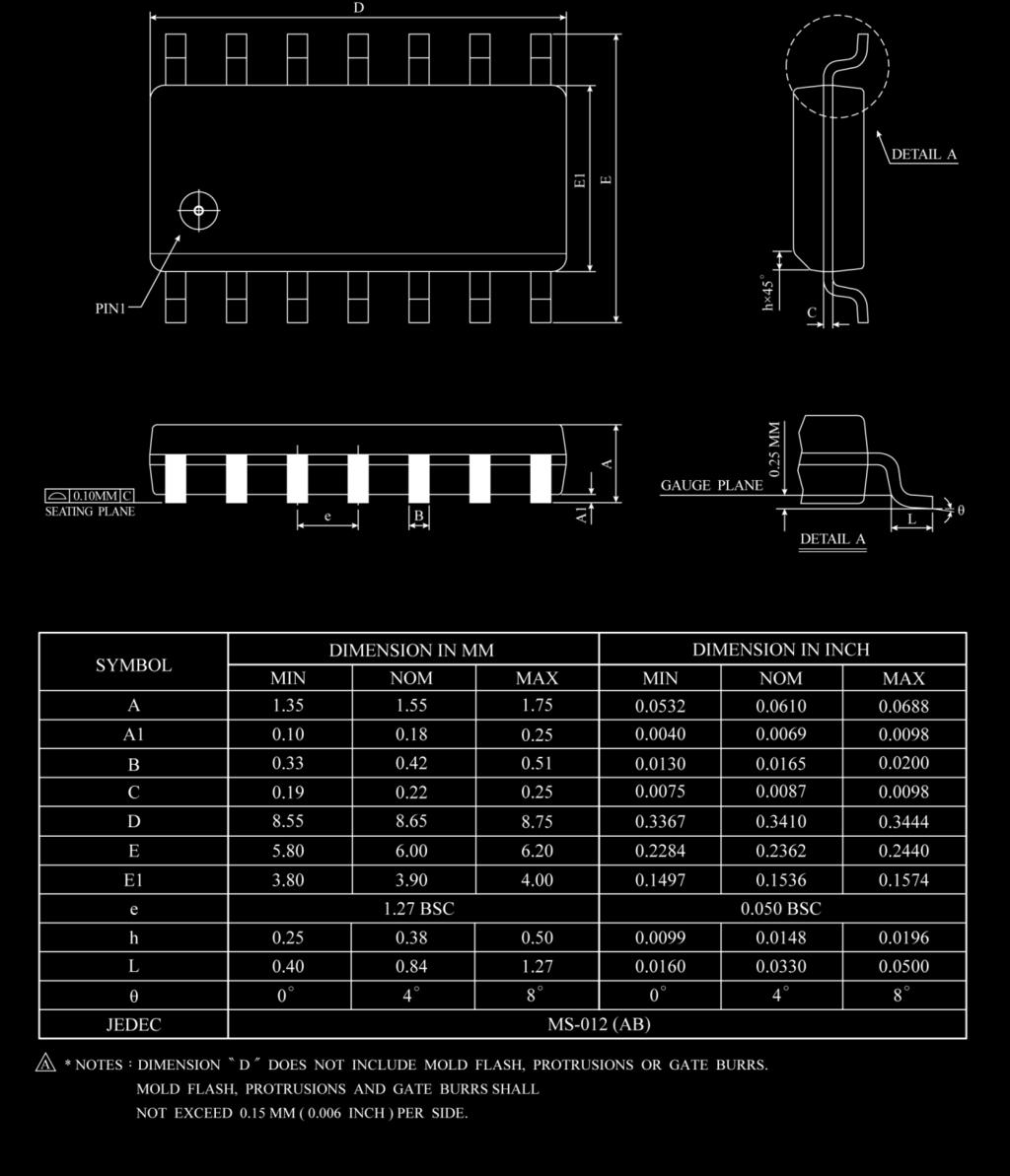
76 SOP-14 ( 150mil ) Package Dimension DS-TM57ME15B_ME15CG_E 76 Rev 0.91, 2018/08/14

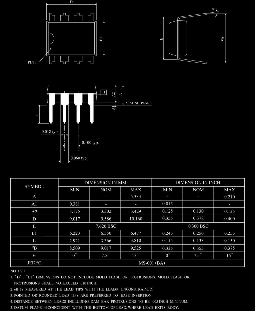
77 DIP-8 ( 300mil ) Package Dimension DS-TM57ME15B_ME15CG_E 77 Rev 0.91, 2018/08/14

78 SOP-8 ( 300mil ) Package Dimension DS-TM57ME15B_ME15CG_E 78 Rev 0.91, 2018/08/14
TM57ME16/18. DATA SHEET Rev 0.95
 TM57ME16/18 DATA SHEET Rev 0.95 tenx reserves the right to change or discontinue the manual and online documentation to this product herein to improve reliability, function or design without further notice.
TM57PE20B. DATA SHEET Rev 0.91
 TM57PE20B DATA SHEET Rev 0.91 tenx reserves the right to change or discontinue the manual and online documentation to this product herein to improve reliability, function or design without further notice.
TM57M5526C/36C. Rev 0.92 DATA SHEET
 TM57M5526C/36C DATA SHEET Rev 0.92 tenx reserves the right to change or discontinue the manual and online documentation to this product herein to improve reliability, function or design without further
TM57M5610/15. DATA SHEET Rev 0.91
 TM57M5610/15 DATA SHEET Rev 0.91 tenx reserves the right to change or discontinue the manual and online documentation to this product herein to improve reliability, function or design without further notice.
TM57PT16/PT16B/PA16. Rev 0.93 DATA SHEET
 TM57PT16/PT16B/PA16 DATA SHEET Rev 0.93 tenx reserves the right to change or discontinue the manual and online documentation to this product herein to improve reliability, function or design without further
TM57PA11. DATA SHEET Rev 1.6
 TM57PA11 DATA SHEET Rev 1.6 tenx reserves the right to change or discontinue the manual and online documentation to this product herein to improve reliability, function or design without further notice.
TP6836. USB 2.4G RF Dongle. Data Sheet
 TP6836 Data Sheet tenx reserves the right to change or discontinue the manual and online documentation to this product herein to improve reliability, function or design without further notice. tenx does
TM57PA20/ TM57PA40. 8 Bit Microcontroller. User Manual. Tenx reserves the right to change or discontinue this product without notice.
 Advance Information TM57PA20/ TM57PA40 User Manual Tenx reserves the right to change or discontinue this product without notice. tenx technology inc. tenx technology, inc. CONTENTS FEATURES... 3 BLOCK
DERTS Design Requirements (1): Microcontroller Architecture & Programming
: Microcontroller Architecture & Programming") Lecture (5) DERTS Design Requirements (1): Microcontroller Architecture & Programming Prof. Kasim M. Al-Aubidy Philadelphia University 1 Lecture Outline: Features of microcomputers and microcontrollers.
Lecture (5) DERTS Design Requirements (1): Microcontroller Architecture & Programming Prof. Kasim M. Al-Aubidy Philadelphia University 1 Lecture Outline: Features of microcomputers and microcontrollers.
TR1002. PLL for DTS IC. Data Sheet
 TR1002 PLL for DTS IC Data Sheet tenx reserves the right to change or discontinue the manual and online documentation to this product herein to improve reliability, function or design without further notice.
EE6008-Microcontroller Based System Design Department Of EEE/ DCE
 UNIT- II INTERRUPTS AND TIMERS PART A 1. What are the interrupts available in PIC? (Jan 14) Interrupt Source Enabled by Completion Status External interrupt from INT INTE = 1 INTF = 1 TMR0 interrupt T0IE
NH-67, TRICHY MAIN ROAD, PULIYUR, C.F , KARUR DT. DEPARTMENT OF ELECTRONICS AND COMMUNICATION ENGINEERING COURSE MATERIAL
 NH-67, TRICHY MAIN ROAD, PULIYUR, C.F. 639 114, KARUR DT. DEPARTMENT OF ELECTRONICS AND COMMUNICATION ENGINEERING COURSE MATERIAL Subject Name : Embedded System Class/Sem : BE (ECE) / VII Subject Code
VREG_3V3 Block User Guide V03.03
 DOCUMENT NUMBER S12VREG3V3V3/D VREG_3V3 Block User Guide V03.03 Original Release Date: 12 Jul 2001 Revised: 12 Jan 2004 Semiconductor Products Sector Motorola, Inc Motorola reserves the right to make changes
SH69P48A EVB. Application Notes for SH69P48A EVB SH69V48A JP2 J4(ICE_J4) S1 IDD TEST JP1 74HC273 JP4 JP3 74HC273 JP6 STKOVE JP7 SW1 J5(ICE_J5)
 S1 IDD TEST JP1 74HC273 JP4 JP3 74HC273 JP6 STKOVE JP7 SW1 J5(ICE_J5)") SH69P48A EVB Application Notes for SH69P48A EVB The SH69P48A EVB is used to evaluate the SH69P48A chip's function for the development of application program. It contains of a SH69V48A chip to evaluate
SH69P48A EVB Application Notes for SH69P48A EVB The SH69P48A EVB is used to evaluate the SH69P48A chip's function for the development of application program. It contains of a SH69V48A chip to evaluate
PIC 16F84A programming (II)
") Lecture (05) PIC 16F84A programming (II) Dr. Ahmed M. ElShafee ١ Introduction to 16F84 ٣ PIC16F84 belongs to a class of 8-bit microcontrollers of RISC architecture. Program memory (FLASH) EEPROM RAM PORTA
Lecture (05) PIC 16F84A programming (II) Dr. Ahmed M. ElShafee ١ Introduction to 16F84 ٣ PIC16F84 belongs to a class of 8-bit microcontrollers of RISC architecture. Program memory (FLASH) EEPROM RAM PORTA
VREG_3V3 Block User Guide V05.03
 nc. DOCUMENT NUMBER S12VREG3V3V5/D VREG_3V3 Block User Guide V05.03 Original Release Date: 12 Jul 2001 Revised: 09 Sep 2004 Semiconductor Products Sector Motorola, Inc Motorola reserves the right to make
Section 11. Timer0. Timer0 HIGHLIGHTS. This section of the manual contains the following major topics:
 M 11 Section 11. HIGHLIGHTS This section of the manual contains the following major topics: 11.1 Introduction...11-2 11.2 Control Register...11-3 11.3 Operation...11-4 11.4 TMR0 Interrupt...11-5 11.5 Using
SH69P55A EVB. Application Note for SH69P55A EVB SH69P55A EVB SH69V55A
 Application Note for SH69P55A EVB SH69P55A EVB The SH69P55A EVB is used to evaluate the SH69P55A chip's function for the development of application program. It contains of a SH69V55A chip to evaluate the
VREG_3V3 Block User Guide V02.03
 DOCUMENT NUMBER S12VREG3V3V2/D VREG_3V3 Block User Guide V02.03 Original Release Date: 12 Jul 2001 Revised: 22 Jun 2004 Semiconductor Products Sector Motorola, Inc Motorola reserves the right to make changes
HT1621. RAM Mapping 32 4 LCD Controller for I/O µc. Features. General Description. Selection Table
 RAM Mapping 32 4 LCD Controller for I/O µc Features Operating voltage : 2.4V~5.2V Built-in 256kHz RC oscillator External 32.768kHz crystal or 256kHz frequency source input Selection of 1/2 or 1/3 bias,
which means that writing to a port implies that the port pins are first read, then this value is modified and then written to the port data latch.
 Introduction to microprocessors Feisal Mohammed 3rd January 2001 Additional features 1 Input/Output Ports One of the features that differentiates a microcontroller from a microprocessor is the presence
SH69P21 EVB. Application Note for SH69P21 EVB SH69P21 EVB SH69P21
 SH69P21 EVB Application Note for SH69P21 EVB The SH69P21 EVB is used to evaluate the SH69P21 chip's function for the development of application program. It contains of a SH69V21 chip to evaluate the functions
============ CONTENTS ============
 ============ CONTENTS ============ 1. INTRODUCTION... 3 2. FEATURES... 3 3. PIN ASSIGNMENT... 4 4. ROM TABLE... 7 5. RAM TABLE... 8 6. SYSTEM CLOCK... 9 6.1 CRYSTAL INPUT... 9 6.2 ROSC INPUT... 9 7. I/O
8051 Microcontroller
 8051 Microcontroller The 8051, Motorola and PIC families are the 3 leading sellers in the microcontroller market. The 8051 microcontroller was originally developed by Intel in the late 1970 s. Today many
MC68HC05J1A/D Rev. 1.0 HC 5 MC68HC05J1A MC68HCL05J1A MC68HSC05J1A. HCMOS Microcontroller Units TECHNICAL DATA
 MC68HC0J1A/D Rev. 1.0 HC MC68HC0J1A MC68HCL0J1A MC68HSC0J1A HCMOS Microcontroller Units TECHNICAL DATA Technical Data Motorola reserves the right to make changes without further notice to any products
UNISONIC TECHNOLOGIES CO., LTD 6621 Preliminary LINEAR INTEGRATED CIRCUIT
 UNISONIC TECHNOLOGIES CO., LTD 6621 Preliminary LINEAR INTEGRATED CIRCUIT RAM MAPPLING 32 4 LCD CONTROLLER FOR I/O μc DESCRIPTION The UTC 6621 is a 128 patterns (32 4), memory mapping, and multi-function
nc. Factors which affect reset are: 1. External components attached to the RESET pin 2. Low-voltage reset (LVR) on chip 3. Power-on reset (POR) detect
 on chip 3. Power-on reset (POR) detect") nc. Order this document by /D Motorola Semiconductor Resetting MCUs By Ross Mitchell MCU Applications Motorola Ltd. East Kilbride, Scotland Introduction A simple function such as reset can cause many problems
nc. Order this document by /D Motorola Semiconductor Resetting MCUs By Ross Mitchell MCU Applications Motorola Ltd. East Kilbride, Scotland Introduction A simple function such as reset can cause many problems
Freescale Semiconductor, I
 M68HC705X4PGMR/D1 August 1991 M68HC705X4 PROGRAMMER BOARD (REVision A PWBs only) INTRODUCTION This application note describes the programming technique used to program and verify the XC68HC705X4 microcontroller
AND9407/D Low Power Techniques of LC Series for Audio Applications
 Low Power Techniques of LC823450 Series for Audio Applications Introduction This application note describes low power techniques to enable customers to control the power consumption to meet their operation
Understanding the basic building blocks of a microcontroller device in general. Knows the terminologies like embedded and external memory devices,
 Understanding the basic building blocks of a microcontroller device in general. Knows the terminologies like embedded and external memory devices, CISC and RISC processors etc. Knows the architecture and
EEE3410 Microcontroller Applications Department of Electrical Engineering Lecture 4 The 8051 Architecture
 Department of Electrical Engineering Lecture 4 The 8051 Architecture 1 In this Lecture Overview General physical & operational features Block diagram Pin assignments Logic symbol Hardware description Pin
SN8F5000 Starter-Kit User Manual
 SONiX Technology Co., Ltd. User Manual 8051-based Microcontroller 1 Overview of Starter Kit provides easy-development platform. It includes SN8F5000 family real chip and I/O connectors to input signal
PIC12C5XX. 8-Pin, 8-Bit CMOS Microcontroller. CMOS Technology: Devices included in this Data Sheet: High-Performance RISC CPU: Pin Diagram
 This document was created with FrameMaker 404 8-Pin, 8-Bit CMOS Microcontroller PIC12C5XX Devices included in this Data Sheet: PIC12C508 and PIC12C509 are 8-bit microcontrollers packaged in 8-lead packages.
PIC16C52. EPROM-Based 8-Bit CMOS Microcontroller PIC16C52. Pin Diagrams. Feature Highlights. High-Performance RISC CPU. Peripheral Features
 This document was created with FrameMaker 404 PIC16C52 EPROM-Based 8-Bit CMOS Microcontroller Feature Highlights Pin Diagrams Program Memory Data Memory I/O PDIP, SOIC 384 25 12 High-Performance RISC CPU
Embedded Systems Design (630470) Lecture 4. Memory Organization. Prof. Kasim M. Al-Aubidy Computer Eng. Dept.
 Lecture 4. Memory Organization. Prof. Kasim M. Al-Aubidy Computer Eng. Dept.") Embedded Systems Design (630470) Lecture 4 Memory Organization Prof. Kasim M. Al-Aubidy Computer Eng. Dept. Memory Organization: PIC16F84 has two separate memory blocks, for data and for program. EEPROM
Embedded Systems Design (630470) Lecture 4 Memory Organization Prof. Kasim M. Al-Aubidy Computer Eng. Dept. Memory Organization: PIC16F84 has two separate memory blocks, for data and for program. EEPROM
Figure 1: TSSOP-24 ( Top View ) Figure 2: TQFN 4x4-24 ( Top View )
 Figure 2: TQFN 4x4-24 ( Top View )") 16-bit I2C-bus and SMBus I/O port with interrupt Features Operation power supply voltage from 2.3V to 5.5V 16-bit I/O pins which can be programmed as Input or Output 5V tolerant I/Os Polarity inversion
16-bit I2C-bus and SMBus I/O port with interrupt Features Operation power supply voltage from 2.3V to 5.5V 16-bit I/O pins which can be programmed as Input or Output 5V tolerant I/Os Polarity inversion
TouchCore351-ML16IP. Capacitive Touch Sensor Controller
 Total Solution of MCU TouchCore351-ML16IP Capacitive Touch Sensor Controller CORERIVER Semiconductor reserves the right to make corrections, modifications, enhancements, improvements, and other changes
EEE111A/B Microprocessors
 EEE111A/B Microprocessors Revision Notes Lecture 1: What s it all About? Covers the basic principles of digital signals. The intelligence of virtually all communications, control and electronic devices
Embedded Systems. PIC16F84A Internal Architecture. Eng. Anis Nazer First Semester
 Embedded Systems PIC16F84A Internal Architecture Eng. Anis Nazer First Semester 2017-2018 Review Computer system basic components? CPU? Memory? I/O? buses? Instruction? Program? Instruction set? CISC,
Features. Description. Applications. Pin Configuration PI4ULS3V Bit Bi-directional Level Shifter for open-drain and Push-Pull Application
 4-Bit Bi-directional Level Shifter for open-drain and Push-Pull Application Features can be Less than, Greater than or Equal to V CCB 1.1V to 3.6V on A Port and 1.1V to 3.6V on B Port High-Speed with 24
SNC Four Channels Speech Controller
 ========================== CONTENTS =========================== 1. INTRODUCTION... 3 2. FEATURES... 3 3. BLOCK DIAGRAM... 4 4. PIN ASSIGNMENT... 5 5. FUNCTION DESCRIPTIONS... 6 5.1. OSCILLATOR... 6 5.2.
M68HC705E6PGMR PROGRAMMER USER'S MANUAL
 M68HC705E6PGMR/D2 nc. Oct 1993 M68HC705E6PGMR PROGRAMMER USER'S MANUAL Motorola reserves the right to make changes without further notice to any products herein to improve reliability, function or design.
HT49R10A-1/HT49C10-1 LCD Type 8-Bit MCU
 LCD Type 8-Bit MCU Technical Document Tools Information FAQs Application Note HA007E Controlling the Read/Write Function of the HT24 Series EEPROM Using the HT49 Series MCUs HA0024E Using the RTC in the
M68HC705E24PGMR PROGRAMMER USER'S MANUAL
 M68HC705E24PGMR/D Rev. 2 March 1995 M68HC705E24PGMR PROGRAMMER USER'S MANUAL Third Edition MOTOROLA Ltd., 1993, 1995; All Rights Reserved Motorola reserves the right to make changes without further notice
PIN DESCRIPTION Name I/O Description VDD P VSS P 5V Power from USB cable Ground RC6M O X1 I Test/OTP mode clock in Internal clock output (6MHz) VPP I
 VPP I") GENERAL DESCRIPTION The IN6005 is an 8-bit microprocessor embedded device tailored to the USB genernal purpose application. It includes an 8-bit RISC CPU core, 192-byte SRAM, Low Speed USB Interface and
GENERAL DESCRIPTION The IN6005 is an 8-bit microprocessor embedded device tailored to the USB genernal purpose application. It includes an 8-bit RISC CPU core, 192-byte SRAM, Low Speed USB Interface and
These 3 registers contain enable, priority,
 8.3.2) Registers Related to Interrupts These registers enable/disable the interrupts, set the priority of the interrupts, and record the status of each interrupt source. RCON INTCON, INTCON2, and INTCON3
Section 8. Reset HIGHLIGHTS. Reset. This section of the manual contains the following major topics:
 Section 8. HIGHLIGHTS This section of the manual contains the following major topics: 8.1 Introduction... 8-2 8.2 Control Registers...8-3 8.3 System...8-6 8.4 Using the RCON Status Bits... 8-11 8.5 Device
EETS2K Block User Guide V01.03
 DOCUMENT NUMBER S12EETS2KV1/D EETS2K Block User Guide V01.03 Original Release Date: 08 JUN 2001 Revised: 09 JUL 2002 Motorola, Inc Motorola reserves the right to make changes without further notice to
Hi Hsiao-Lung Chan Dept Electrical Engineering Chang Gung University, Taiwan
 Interrupts and Resets Hi Hsiao-Lung Chan Dept Electrical Engineering Chang Gung University, Taiwan chanhl@mail.cgu.edu.twcgu Interrupts An event that will cause the CPU to stop the normal program execution
EU bit MCU with 10-bit A/D Converter. Features. Description. Ordering Information
 8-bit MCU with 10-bit A/D Converter Features 2.2V to 5.5V Input Voltage Range 14 I/O ports in RAM size: 128 x 8 bits The STACK RAM is included. Program ROM size: 4K x 8 bits OTP 10 bits A/D Converter input
3. Applications. 1. General Description. 4. Pin Assignment. 2. Features M D T10P509ST2611 PB0 1 6 PB3 M D T10P509ST2613 PB0 1 6 /MCLR
 M MDT10P509 D P509(A) T 1 0P50 1. General Description 3. Applications This EPROM-Based 8-bit micro-controller uses a fully static CMOS technology process to achieve higher speed and smaller size with the
HT48R30A-1/HT48C30-1 I/O Type 8-Bit MCU
 I/O Type 8-Bit MCU Features Operating voltage: f SYS =4MHz: 2.2V~5.5V f SYS =8MHz: 3.3V~5.5V Low voltage reset function 25 bidirectional I/O lines (max.) interrupt input shared with an I/O line 8-bit programmable
SONIX 8-BIT MCU OTP Easy Writer
 SONIX 8-BIT MCU OTP Easy Writer User s Manual General Release Specification SONIX reserves the right to make change without further notice to any products herein to improve reliability, function or design.
Section 13. Timer0 HIGHLIGHTS. Timer0. This section of the manual contains the following major topics:
 Section 13. Timer0 HIGHLIGHTS This section of the manual contains the following major topics: 13.1 Introduction... 13-2 13.2 Control Register... 13-3 13.3 Operation... 13-4 13.4 Timer0 Interrupt... 13-5
PIC Microcontroller Introduction
 PIC Microcontroller Introduction The real name of this microcontroller is PICmicro (Peripheral Interface Controller), but it is better known as PIC. Its first ancestor was designed in 1975 by General Instruments.
PIC10F200/202/204/206 Data Sheet
 Data Sheet 6-Pin, 8-Bit Flash Microcontrollers DS4239A 6-Pin, 8-Bit Flash Microcontrollers Devices Included In ThisData Sheet: PIC0F200 PIC0F202 PIC0F204 PIC0F206 High-Performance RISC CPU: Only 33 single-word
CENG-336 Introduction to Embedded Systems Development. Timers
 CENG-336 Introduction to Embedded Systems Development Timers Definitions A counter counts (possibly asynchronous) input pulses from an external signal A timer counts pulses of a fixed, known frequency
Section 28. WDT and SLEEP Mode
 Section 28. WDT and SLEEP Mode HIGHLIGHTS This section of the manual contains the following major topics: 28 28.1 Introduction... 28-2 28.2 Control Register... 28-3 28.3 Watchdog Timer (WDT) Operation...
PIC16C84. 8-bit CMOS EEPROM Microcontroller PIC16C84. Pin Diagram. High Performance RISC CPU Features: CMOS Technology: Peripheral Features:
 8-bit CMOS EEPROM Microcontroller High Performance RISC CPU Features: Only 35 single word instructions to learn All instructions single cycle (400 ns @ 10 MHz) except for program branches which are two-cycle
PIC10F200/202/204/206
 6-Pin, 8-Bit Flash Microcontrollers Devices Included In This Data Sheet: PIC0F200 PIC0F202 PIC0F204 PIC0F206 High-Performance RISC CPU: Only 33 Single-Word Instructions to Learn All Single-Cycle Instructions
M68EM05X4 EMULATOR MODULE USER'S MANUAL
 M68EM05X4/D Rev. 2 January 1996 M68EM05X4 EMULATOR MODULE USER'S MANUAL Third Edition MOTOROLA Ltd., 1993, 1995, 1996; All Rights Reserved Motorola reserves the right to make changes without further notice
HT46R53A/HT46R54A A/D Type 8-Bit OTP MCU
 A/D Type 8-Bit OTP MCU Features Low-power fully static CMOS design Operating voltage: f SYS =4MHz: 2.2V~5.5V f SYS =8MHz: 3.3V~5.5V Program Memory: 2K5 OTP (HT46R53A) 4K5 OTP (HT46R54A) Data memory: 928
8-bit Microcontroller with 8K Bytes In-System Programmable Flash AT89S52
 Features Compatible with MCS -51 Products 8K Bytes of In-System Programmable (ISP) Flash Memory Endurance: 10,000 Write/Erase Cycles 4.0V to 5.5V Operating Range Fully Static Operation: 0 Hz to 33 MHz
Pin Assignment 2 ) # 2 ) % 2 ) $ 2 )! 2 ) 6 2 ) 2 )! " 4 # $ % /, & ' ' & % $ # "! 2 ) " : /, * ) 6 8,, * $ * 2 ) # 2 ) %
 # 2 ) % 2 ) $ 2 )! 2 ) 6 2 ) 2 )! 4 # $ % /, & ' ' & % $ # ! 2 ) : /, * ) 6 8,, * $ * 2 ) # 2 ) %") RF One Channel Mouse 8-bit OTP MCU Technical Document Tools Information FAQs Application Note HA0075E MCU Reset and Oscillator Circuits Application Note Features Operating voltage: f SYS = 27MHz: 2.0V~3.3V
RF One Channel Mouse 8-bit OTP MCU Technical Document Tools Information FAQs Application Note HA0075E MCU Reset and Oscillator Circuits Application Note Features Operating voltage: f SYS = 27MHz: 2.0V~3.3V
SNL16000 MTP EV chip (with 2Mx16 Flash Memory)
") ================== CONTENTS ================= 1. INRODUCTION... 3 2. FEATURES... 3 2.1. CPU... 3 2.2. WPU... 4 2.3. LCD... 4 3. FLASH MEMORY... 6 4. RAM... 6 5. PIN ASSIGNMENT... 7 6. LQFP-256 OUTLINE...
================== CONTENTS ================= 1. INRODUCTION... 3 2. FEATURES... 3 2.1. CPU... 3 2.2. WPU... 4 2.3. LCD... 4 3. FLASH MEMORY... 6 4. RAM... 6 5. PIN ASSIGNMENT... 7 6. LQFP-256 OUTLINE...
Section 8. Reset. Reset HIGHLIGHTS. This section of the manual contains the following topics:
 Section 8. HIGHLIGHTS This section of the manual contains the following topics: 8.1 Introduction... 8-2 8.2 Clock Source Selection at... 8-5 8.3 POR: Power-on... 8-5 8.4 External (EXTR)... 8-7 8.5 Software
TP6825. USB Full Speed Game Pad Controller. Data Sheet. Tenx reserves the right to change or discontinue this product without notice.
 Advance Information TP6825 USB Full Speed Game Pad Controller Data Sheet Tenx reserves the right to change or discontinue this product without notice. tenx technology, inc. Contain 1. GENERAL DESCRIPTION...
PMC153/PMS153 Series 8-bit IO-Type Controller
 Datasheet Version 0.06 July 7, 2016 Copyright 2016 by PADAUK Technology Co., Ltd., all rights reserved 10F-2, No. 1, Sec. 2, Dong-Da Road, Hsin-Chu 300, Taiwan, R.O.C. TEL: 886-3-532-7598 www.padauk.com.tw
PMC153/PMS153 Series 8-bit OTP Type IO Controller
 Datasheet Version 1.07 Dec. 11, 2018 Copyright 2018 by PADAUK Technology Co., Ltd., all rights reserved 6F-6, No.1, Sec. 3, Gongdao 5th Rd., Hsinchu City 30069, Taiwan, R.O.C. TEL: 886-3-572-8688 www.padauk.com.tw
SNC36060 Four Channels Speech Controller
 ========================== CONTENTS =========================== 1. INTRODUCTION... 3 2. FEATURES... 3 3. BLOCK DIAGRAM... 4 4. PIN ASSIGNMENT... 5 5. FUNCTION DESCRIPTIONS... 6 5.1. OSCILLATOR... 6 5.2.
M68HC08 Microcontroller The MC68HC908GP32. General Description. MCU Block Diagram CPU08 1
 M68HC08 Microcontroller The MC68HC908GP32 Babak Kia Adjunct Professor Boston University College of Engineering Email: bkia -at- bu.edu ENG SC757 - Advanced Microprocessor Design General Description The
Embedded System Design
 ĐẠI HỌC QUỐC GIA TP.HỒ CHÍ MINH TRƯỜNG ĐẠI HỌC BÁCH KHOA KHOA ĐIỆN-ĐIỆN TỬ BỘ MÔN KỸ THUẬT ĐIỆN TỬ Embedded System Design : Microcontroller 1. Introduction to PIC microcontroller 2. PIC16F84 3. PIC16F877
RW1026G Revision History Version Date Description
 RW1026G Revision History Version Date Description 0.1 2010/9/3 Add I/O Pin ITO Resistance Limitation 0.2 2010/9/15 Modify storage temperature -40 o C to 80 o C change to -50 o C to 125 o C and operation
EETS4K Block User Guide V02.06
 DOCUMENT NUMBER S12EETS4KV2/D EETS4K Block User Guide V02.06 Original Release Date: 22 FEB 2001 Revised: 23 JAN 2003 Motorola, Inc Motorola reserves the right to make changes without further notice to
Lecture (02) PIC16F84 (I)
 PIC16F84 (I)") Lecture (02) PIC16F84 (I) By: Dr. Ahmed ElShafee ١ Review of Memory Technologies The PIC 16 Series PIC 16F84A The PIC 16F84A Memory The Oscillator Instruction Cycle Power up and Reset Parallel ports Technical
Lecture (02) PIC16F84 (I) By: Dr. Ahmed ElShafee ١ Review of Memory Technologies The PIC 16 Series PIC 16F84A The PIC 16F84A Memory The Oscillator Instruction Cycle Power up and Reset Parallel ports Technical
PMC156/PMS156 Series 8-bit IO-Type Controller
 Data Sheet Version 0.05 July 07, 2016 Copyright 2016 by PADAUK Technology Co., Ltd., all rights reserved 10F-2, No. 1, Sec. 2, Dong-Da Road, Hsin-Chu 300, Taiwan, R.O.C. TEL: 886-3-532-7598 www.padauk.com.tw
PIC16F8X. 8-Bit CMOS Flash/EEPROM Microcontrollers PIC16F8X PIC16CR8X. Pin Diagram. Devices Included in this Data Sheet:
 This document was created with FrameMaker 404 PIC16F8X 8-Bit CMOS Flash/EEPROM Microcontrollers Devices Included in this Data Sheet: PIC16F83 PIC16CR83 PIC16F84 PIC16CR84 Extended voltage range devices
PMC150/PMS150 Series 8-bit OTP Type IO Controller
 8-bit OTP Type IO Controller Data Sheet Version 1.08 Dec. 11, 2018 Copyright 2018 by PADAUK Technology Co., Ltd., all rights reserved 6F-6, No.1, Sec. 3, Gongdao 5th Rd., Hsinchu City 30069, Taiwan, R.O.C.
M PIC16F84A. 18-pinEnhanced FLASH/EEPROM 8-Bit Microcontroller. High Performance RISC CPU Features: Pin Diagrams. Peripheral Features:
 M PIC6F84A 8-pinEnhanced FLASH/EEPROM 8-Bit Microcontroller High Performance RISC CPU Features: Pin Diagrams Only 35 single word instructions to learn All instructions single-cycle except for program branches
Micro II and Embedded Systems
 16.480/552 Micro II and Embedded Systems Introduction to PIC Microcontroller Revised based on slides from WPI ECE2801 Moving Towards Embedded Hardware Typical components of a PC: x86 family microprocessor
PTK8756B 8 Bit Micro-controller Data Sheet
 PTK8756B 8 Bit Micro-controller DEC 15, 2008 Ver1.1 普泰半導體股份有限公司 PORTEK Technology Corporation 公司地址 : 臺北縣新店市寶橋路 235 巷 120 號 4 樓 聯絡電話 : 886-2-89121055 傳真號碼 : 886-2-89121473 公司網址 : www.portek.com.tw Page1
PIC16F87X 13.0 INSTRUCTION SET SUMMARY INSTRUCTIONS DESCRIPTIONS
 PIC6F87X 3.0 INSTRUCTION SET SUMMARY Each PIC6F87X instruction is a 4bit word, divided into an OPCODE which specifies the instruction type and one or more operands which further specify the operation of
HT48F70E I/O Flash Type MCU with EEPROM
 I/O Flash Type MCU with EEPROM Features Operating voltage: f SYS =4MHz: 2.2V~5.5V f SYS =8MHz: 3.3V~5.5V f SYS =12MHz: 4.5V~5.5V Multi-programmable Flash Type Program Memory: 819216 EEPROM Data Memory:
HT48F06E/HT48F10E/HT48F30E I/O Flash Type MCU with EEPROM
 I/O Flash Type MCU with EEPROM Features Operating voltage: f SYS =4MHz: 2.2V~5.5V f SYS =8MHz: 3.3V~5.5V f SYS =12MHz: 4.5V~5.5V Multi-programmable Flash Type Program Memory EEPROM data memory: 128 8 From
HT1628 RAM Mapping LCD Driver
 RAM Mapping 116 2 LCD Driver Features Logic voltage 2.4V~5.5V LCD operating voltage (VLCD) 2.4V~5.5V LCD display 2 commons, 116 segments Support a maximum of 58 4 bit Display RAM Duty Static, 1/2; Bias
MDT90P General Description. 3. Applications. 2. Features. 4. Pin Assignment
 . General Description Sleep Mode for power saving This EPROM-Based 4-bit micro-controller uses a fully static CMOS technology process to achieve higher speed and smaller size with the low power consumption
8-bit Microcontroller with 1K Bytes Flash. ATtiny10 ATtiny11 ATtiny12. Preliminary. Features. Pin Configuration
 Features Utilizes the AVR RISC Architecture High-performance and Low-power 8-bit RISC Architecture 90 Powerful Instructions - Most Single Clock Cycle Execution 32 x 8 General Purpose Working Registers
Reset Output. Active high Active low Active high Active low
 Low Power Voltage Detector Features High accuracy: 2% (25 C) Low power consumption: 0.6μA @ 3V Vcc Detecting voltage range: 1.8 to 5V in 100mV increments Operating voltage range: 1.2V ~ 5.5V Operating
PIC16C Pin, 8-Bit CMOS Microcontroller. Device included in this Data Sheet: Special Microcontroller Features: High-Performance RISC CPU:
 14-Pin, 8-Bit CMOS Microcontroller Device included in this Data Sheet: PIC16C505 High-Performance RISC CPU: Only 33 instructions to learn Operating speed: - DC - 20 MHz clock input - DC - 200 ns instruction
Microprocessors & Interfacing
 Lecture Overview Microprocessors & Interfacing Interrupts (I) Lecturer : Dr. Annie Guo Introduction to Interrupts Interrupt system specifications Multiple sources of interrupts Interrupt priorities Interrupts
Designed to GO... Universal Battery Monitor Using the bq2018 Power Minder IC. Typical Applications. Features. Figure 1. bq2018 Circuit Connection
 Designed to GO... Practical and Cost-Effective Battery Management Design Examples by Benchmarq Series 2018, Number One Universal Battery Monitor Using the bq2018 Power Minder IC Features Counts charge
8-bit Microcontroller with 1K Byte of In-System Programmable Flash AT90S1200
 Features Utilizes the AVR RISC Architecture AVR High-performance and Low-power RISC Architecture 89 Powerful Instructions Most Single Clock Cycle Execution 32 x 8 General-purpose Working Registers Up to
DHANALAKSHMI COLLEGE OF ENGINEERING, CHENNAI DEPARTMENT OF ELECTRICAL AND ELECTRONICS ENGINEERING. EE6008 Microcontroller based system design
 Year: IV DHANALAKSHMI COLLEGE OF ENGINEERING, CHENNAI DEPARTMENT OF ELECTRICAL AND ELECTRONICS ENGINEERING EE6008 Microcontroller based system design Semester : VII UNIT I Introduction to PIC Microcontroller
FLASH: FASTER WAIT MODE WAKEUP RECOVERY TIME FOR FLASH AR457 ATD: CONVERSION OF THE (V RH V RL )/2 INTERNAL REF VOLTAGE RETURNS $7F, $80 OR $81
/2 INTERNAL REF VOLTAGE RETURNS $7F, $80 OR $81") MOTOROLA SEMICONDUCTOR TECHNICAL INFORMATION 68HC912BC32MSE1 Rev 1 March 1, 2001 Mask Set Errata 1 MC68HC912BC32 Microcontroller Unit INTRODUCTION This errata provides mask-set specific information applicable
MOTOROLA SEMICONDUCTOR TECHNICAL INFORMATION 68HC912BC32MSE1 Rev 1 March 1, 2001 Mask Set Errata 1 MC68HC912BC32 Microcontroller Unit INTRODUCTION This errata provides mask-set specific information applicable
PIC16F8X 18-pin Flash/EEPROM 8-Bit Microcontrollers
 18-pin Flash/EEPROM 8-Bit Microcontrollers Devices Included in this Data Sheet: PIC16F83 PIC16F84 PIC16CR83 PIC16CR84 Extended voltage range devices available (PIC16LF8X, PIC16LCR8X) High Performance RISC
Section 30. In-Circuit Serial Programming (ICSP )
") Section 30. In-Circuit Serial Programming (ICSP ) HIGHLIGHTS This section of the manual contains the following major topics: 30. Introduction... 30-2 30.2 Entering In-Circuit Serial Programming Mode...
Section 30. In-Circuit Serial Programming (ICSP ) HIGHLIGHTS This section of the manual contains the following major topics: 30. Introduction... 30-2 30.2 Entering In-Circuit Serial Programming Mode...
Section 14. Timer1 HIGHLIGHTS. Timer1. This section of the manual contains the following major topics:
 Section 14. Timer1 HIGHLIGHTS This section of the manual contains the following major topics: 14.1 Introduction... 14-2 14.2 Control Register... 14-4 14.3 Timer1 Operation in Timer Mode... 14-5 14.4 Timer1
8-bit Microcontroller with 2K Bytes of Flash. ATtiny28L ATtiny28V
 Features Utilizes the AVR RISC Architecture AVR High-performance and Low-power RISC Architecture 90 Powerful Instructions Most Single Clock Cycle Execution 32 x 8 General-purpose Working Registers Up to
Lecture (04) PIC16F84A (3)
 PIC16F84A (3)") Lecture (04) PIC16F84A (3) By: Dr. Ahmed ElShafee ١ Central Processing Unit Central processing unit (CPU) is the brain of a microcontroller responsible for finding and fetching the right instruction which
Lecture (04) PIC16F84A (3) By: Dr. Ahmed ElShafee ١ Central Processing Unit Central processing unit (CPU) is the brain of a microcontroller responsible for finding and fetching the right instruction which
Interrupts (I) Lecturer: Sri Notes by Annie Guo. Week8 1
 Lecturer: Sri Notes by Annie Guo. Week8 1") Interrupts (I) Lecturer: Sri Notes by Annie Guo Week8 1 Lecture overview Introduction to Interrupts Interrupt system specifications Multiple Sources of Interrupts Interrupt Priorities Interrupts in AVR
Interrupts (I) Lecturer: Sri Notes by Annie Guo Week8 1 Lecture overview Introduction to Interrupts Interrupt system specifications Multiple Sources of Interrupts Interrupt Priorities Interrupts in AVR