Concepts of Digital Design Introduction to Verilog
|
|
|
- Gillian Harris
- 5 years ago
- Views:
Transcription
1 Concepts of Digital Design Introduction to Verilog Nikos Bellas Computer and Communications Engineering Department University of Thessaly 1
2 The Verilog Language A hardware description language (HDL) used for modeling, simulation and synthesis of digital electronic systems One of the two most commonly-used languages in digital hardware design (VHDL is the other) Virtually every chip (FPGA, ASIC, etc.) is designed in part using one of these two languages Combines structural and behavioral modeling styles IEEE standard Verilog-2001 extends the initial Verilog-95 specification 2
3 Simulation Simulation is used to verify the functional characteristics of models at any level of abstraction One of the main uses of Verilog/VHDL is simulation To test if the RTL code meets the functional requirements of the specification, we must see if all the RTL blocks are functionally correct. To achieve this we need to write a testbench, which generates clk, reset and the required test vectors Simulation is needed after every refinement step Behavioral, zero-delay gate level, timing, post P&R simulation 3
4 Discrete-event Simulation Basic idea: only do work when something changes Centered around an event queue Contains events labeled with the simulated time at which they are to be executed Basic simulation paradigm Execute every event for the current simulated time Doing this changes system state and may schedule events in the future When there are no events left at the current time instance, advance simulated time soonest event in the queue 4
5 How Are Simulators Used? Testbench generates stimulus and checks response Coupled to model of the system Pair is run concurrently Stimulus Testbench System Under Test Result checker Response 5
6 Timing Simulation Timing simulation occurs after synthesis and after Place and Route (P&R) It includes gate and wire delays to make simulation more realistic Before P&R, the simulator uses gate delays models and (if available) wire delay models After P&R, more detailed wire delay information can be fed back to the simulator 6
7 Synthesis High level (behavioral) synthesis (HLS) is the conversion from algorithmic/behavioral logic to synthesizable HDL The input to the HLS tool is C, C++, SystemC, behavioral HDL, etc. HLS consists of the following steps Parsing and analysis Algorithmic optimization Control/Data flow analysis Operation scheduling Resource allocation and binding Code generation 7
8 Synthesis Logic synthesis is the conversion from synthesizable HDL or from boolean functions to a multilevel gate netlist First, technology-independent optimizations based on boolean arithmetic properties Then, technology dependent optimizations convert the circuit into a network of gates in a given technology Library mapping uses the available technology libraries to map boolean expression into gates 8
9 Placement and Routing (ASIC) The gate level netlist is then placed in the 2D available space and the gate blocks are interconnected The objective is to reduce latency and improve clock frequency Clock tree synthesis also happens here The P&R tool output is a GDSII file, used by foundry for fabricating the ASIC GDSII is data base format used for data exchange of integrated circuit or IC layout artwork 9
10 Placement and Routing (FPGA) FPGAs contain programmable logic blocks that can be reconfigured by the user after fabrication Placement maps the synthesized gate netlist into the available reconfigurable logic Routing maps the interconnects between gates into the available routing resources of the FPGA After P&R, a tool is used to produce the final configuration bitstream The bitstream is loaded to configure the FPGA 10
-bit result 1101 +0101 10010 Ripplecarry adder 11")
11 Learn by Example: Combinational Logic Adder: a circuit that does addition Here s an example of binary addition: Adding two N-bit numbers produces an (N+1)-bit result Ripplecarry adder 11
12 1-bit Adder Build Truth Table and use Sum of Products (SOP) Α Β Cin S Cout Sum: S A B C Carry Out: CO A'BC AB'C ABC' ABC (A' A)BC (B' B)AC AB(C' C) BC AC AB 12
13 1-bit Adder module: Basic unit of description One line comment // This is a behavioral module of 1-bit adder module fulladd (Cin, x, y, s, Cout); input Cin, x, y; output s, Cout; assign s = x ^ y ^ Cin; assign Cout = (x & y) (x & Cin) (y & Cin); I/O ports with which the module communicates externally with other modules endmodule Continuous assignment: the RHS is evaluated again every time the value of an operand changes. The LHS is assigned that value. This is an example of Behavioral Description 13
14 4-bit Adder Structural Description /* This is a structural module of 1-bit adder */ module adder4 (carryin, X, Y, S, carryout); input carryin; input [3:0] X, Y; output [3:0] S; output carryout; wire [3:1] C; Multiple lines comment Instantiation of the module fulladd Arguments correspond to formal parameters of modules fulladd stage0 (carryin, X[0], Y[0], S[0], C[1]); fulladd stage1 (C[1], X[1], Y[1], S[1], C[2]); fulladd stage2 (C[2], X[2], Y[2], S[2], C[3]); fulladd stage3 (C[3], X[3], Y[3], S[3], carryout); endmodule 14
15 Alternative N-bit Adder module addern #(parameter n=32) (carryin, X, Y, S, carryout); input carryin; input [n-1:0] X, Y; output [n-1:0] S; output carryout; reg is a data type that indicates a reg [n-1:0] S; driver that can store a value. reg carryout; If a signal is not reg, it is a wire reg [n:0] C; integer k; n=32 sets default value for parameter n An always statement is only triggered at (@) the condition in the parenthesis (sensitivity list). We execute the always statement only when X or Y or carryin change Y, carryin) begin C[0] = carryin; for (k = 0; k < n; k = k+1) begin S[k] = X[k] ^ Y[k] ^ C[k]; C[k+1] = (X[k] & Y[k]) (X[k] & C[k]) (Y[k] & C[k]); end carryout = C[n]; end endmodule Behavioral Description 15
16 module addern #(paramtere n=32) (carryin, X, Y, S, carryout, overflow); input carryin; input [n-1:0] X, Y; output [n-1:0] S; output carryout, overflow; reg [n-1:0] S; S, X, Y are arrays reg carryout, overflow; or Y or carryin) begin S = X + Y + carryin; carryout = (X[n-1] & Y[n-1]) (X[n-1] & ~S[n-1]) (Y[n-1] & ~S[n-1]); overflow = carryout ^ X[n-1] ^ Y[n-1] ^ S[n-1]; end endmodule Another one Behavioral Description 16
17 Sequential Logic 17
18 Specifications What if you were given the following design specification: button When the button is pushed: 1)Turn on the light if it is off 2)Turn off the light if it is on The light should change state within a second of the button press light What makes this circuit different from those we ve discussed before? 1. State i.e. the circuit has memory 2.The output was changed by a input event (pushing a button) rather than an input value c 18
 OUTPUT bit (from input, current state) State changes on LOAD control input If Output depends on Input and current")
19 Digital State One model of what we d like to build Memory Device LOAD Current State Combinational Logic New State Input Output Plan: Build a Sequential Circuit with stored digital STATE Memory stores CURRENT state Combinational Logic computes NEXT state (from input, current state) OUTPUT bit (from input, current state) State changes on LOAD control input If Output depends on Input and current state, circuit is called a Mealy machine. If Output depends only on the current state, circuit is called a Moore machine. 19
20 Our building block: the D FF The edge-triggered D register: on the rising edge of CLK, the value of D is saved in the register and then shortly afterwards appears on Q. D CLK Q 20
21 D-Register Timing t PD t CD Q CLK D t PD : maximum propagation delay, CLK Q t CD : minimum contamination delay, CLK Q t SETUP : setup time How long D must be stable before the rising edge of CLK t HOLD : hold time How long D must be stable after the rising edge of CLK t SETUP t HOLD 21
22 The Sequential always Block module dff (input D, CLK, output reg Q); clk) begin Q<=D; end endmodule; module CL(input a,b, sel, output reg out); begin if (sel) out = b; else out = a; end endmodule; module SL(input a,b, sel, output reg out); clk) begin if (sel) out = b; else out = a; end endmodule; 22
23 Language Elements and Expressions 23
24 Numbers in Verilog Integer numbers Simple decimal notation 32, -15 Base format notation : [size in bits] base value Base is one of d or D (decimal), o or O (octal), b or B (binary), h or H (hex). Use s for signed. 5 O37 // 5 bit octal number 37 4 D2 // 4 bit decimal number 2 4 B1x_01 // 4 bit binary number 1x01. 7 Hx // 7 bit hex xxxxxxx 8 shff // Signed hex equal to -1 4 d-4 // Not legal. The sign is before the size. -4 d4 // 4-bit binary number -4. The sign is before the size (2+3)d 10 // Not legal. Size cannot be an expression The underscore character (_) is legal anywhere in a number except as the first character, where it is ignored When used in a number, the question mark (?) character is the Verilog alternative for the z character. 24
25 Numbers in Verilog Real numbers Decimal notation 32.0, // Not legal. Must have a digit on either side of decimal Scientific notation 23.51e2 // _5.1e1 // E-4 25
26 Strings in Verilog A string is a sequence of chars within double quotes Verilog is cool! 26
27 Four-valued Data Verilog s nets and registers hold four-valued data 0, 1 Obvious Z (high impedance) Output of an undriven tri-state driver Models case where nothing is setting a wire s value X (unknown or undecided) Models when the simulator can t decide the value Initial state of registers When a wire is being driven to 0 and 1 simultaneously Output of a gate with Z inputs 27
28 Two Main Data Types Wires represent connections between things Do not hold their value Take their value from a driver such as a gate or other module A signal is wire by default Regs represent data storage Behave exactly like memory in a computer Hold their value until explicitly assigned in an initial or always block Can be used to model latches, flip-flops, etc., but do not correspond exactly Shared variables with all their attendant problems 28
29 Nets and Registers Wires and registers can be bits, vectors, and arrays wire a; // Simple wire wire [15:0] dbus; // 16-bit bus wire #(5,4,8) b; // Wire with rise delay 5, fall delay 4, and turn-off delay (hiz) 8 reg [-1:4] vec; // Six-bit register integer imem[0:1023]; // Array of 1024 integers reg [31:0] dcache[0:63]; // A 32-bit mem with 64 entries 29
30 Operators Arithmetic operators X = (A+B)-C // binary plus and minus X = -Y // unary minus X = Y*Z // multiplication X = A/B // division X = A%B // modulus is the remainder with // the sign of the dividend. // 7%4 = 3, -7%4 = -3, 7%-4 = 3 X = A**B // exponent (Only in Verilog 2001) 30
31 Relational operators Operators The result is 0 (false), 1 (true), or x (either operand has an x or z bit) 23 > 45 // false (value 0) 52 < 8 hxff // result is x b1000 >= b01110 // false. Smaller sized operand is zero-filled 31
32 Equality operators. Operators 2 b10 == 4 b0010 // true b11x0 == b11x0 // unknown because there is a bit in in either operand which is x (or z) b11x0 === b11x0 // true. In case equality, x and z are compared strictly as values 32
33 Logical operators. Operators A && B // logical AND A B // logical OR!A // logical NOT 33
34 Bit-wise operators ~A (unary negation) & (binary and) (binary or) ^ (binary xor) ~^ (binary XNOR) Operators AND (&) OR (I) 0 1 X Z X X X 0 X X X Z 0 X X X 0 1 X Z X X X X 1 X X Z X 1 X X 34
35 Reduction operators Operators A = b0110, B = b0100, C = b0x1 &B is 0 // logical AND of all bits B is 1 // logical OR of all bits ~&A is 1 // logical NAND of all bits ^B is 1 // logical XOR of all bits ~^B is 0 // logical XNOR of all bits &C is 0 // at least a bit is 0 C is 1 // at least a bit is 1 ^C is x // if any bit is x or z, result is x 35
36 Shift operators Operators A >> B // logical right shift A << B // logical left shift A >>> B // right shift for signed numbers (Only Verilog 2001) A <<< B // left shift for signed numbers (Only Verilog 2001) Conditional operator cond_expr? expr1 : expr2 36
37 Operators Concatenation and Replication operators wire [7:0] Dbus wire [11:0] Abus assign Dbus = {Dbus[3:0], Dbus[7:4]} // concatenation: swap nibbles Abus ={3{4 b1011}} // 12 b1011_1011_
38 Structural and Behavioral Models 38
39 Two Main Components of Verilog Concurrent, event-triggered processes (behavioral) Initial and Always blocks Imperative code that can perform standard data manipulation tasks (assignment, if-then, case) Processes run until they delay for a period of time or wait for a triggering event Structure (structural) Verilog program built from modules with I/O interfaces Modules may contain instances of other modules Modules contain local signals, etc. Module configuration is static and all run concurrently High level modules typically structural Low level modules (leaves) typically behavioral 39
40 Structural Modeling When Verilog was first developed (1984) most logic simulators operated on netlists Netlist: list of gates and how they re connected A natural representation of a digital logic circuit Not the most convenient way to express test benches 40
41 Behavioral Modeling A much easier way to write testbenches Also good for more abstract models of circuits Easier to write Simulates faster More flexible Provides sequencing Verilog succeeded in part because it allowed both the model and the testbench to be described together 41
42 Multiplexer Built From Primitives module mux(f, a, b, sel); output f; input a, b, sel; Predefined module types and g1(f1, a, nsel), g2(f2, b, sel); or g3(f, f1, f2); not g4(nsel, sel); endmodule sel a b g4 Identifiers not explicitly defined default to wires Module may contain structure: instances of primitives and other modules nsel g1 g2 f1 f2 g3 f 42
43 Multiplexer Built With Always module mux(f, a, b, sel); output f; input a, b, sel; reg f; b, sel) if (sel) f = b; else f = a; endmodule sel a b Modules may contain one or more always blocks Sensitivity list contains signals whose change triggers the execution of the block f 43
44 Mux with Continuous Assignment module mux(f, a, b, sel); output f; input a, b, sel; LHS is always set to the value on the RHS Any change on the right causes reevaluation assign f = sel? b : a; endmodule sel a b f 44
45 Mux with User-Defined Primitive primitive mux(f, a, b, sel); output f; input a, b, sel; table 1?0 : 1; 0?0 : 0;?11 : 1;?01 : 0; 11? : 1; 00? : 0; endtable endprimitive sel a b Behavior defined using a truth table that includes don t cares This is a less pessimistic than others: when a & b match, sel is ignored (others produce X) f 45
46 Structural Modeling 46
47 Modules and Instances Basic structure of a Verilog module: module mymod(port1, port2, portn); output port1; output [3:0] port2; input [2:0] portn; endmodule Verilog convention lists outputs first. This is not necessary 47
48 Modules and Instances Verilog 2001 allows port direction and data type in the port list of modules as shown in the example below module mymod(output port1, output [3:0] port2, input [2:0] portn); endmodule 48
49 Instantiating a Module Instances of module mymod(y, a, b); look like mymod mm1(y1, a1, b1); // Connect-by-position mymod (y2, a1, b1), (y3, a2, b2); // Instance names omitted mymod mm2(.a(a2),.b(b2),.y(c2)); // Connect-by-name 49
50 Gate-level Primitives Verilog provides the following keywords for gate level modeling: and nand logical AND/NAND or nor logical OR/NOR xor xnor logical XOR/XNOR buf not buffer/inverter bufif0 notif0 Tristate buf with low enable bifif1 notif1 Tristate buf with high enable 50
51 Delays on Primitive Instances Instances of primitives may include delays buf b1(a, b); // Zero delay buf #3 b2(c, d); // Delay of 3 buf #(4,5) b3(e, f); // Rise=4, fall=5 buf #(3:4:5) b4(g, h); // Min-typ-max values of all delays 51
52 Switch-level Primitives Verilog also provides mechanisms for modeling CMOS transistors that behave like switches A more detailed modeling scheme that can catch some additional electrical problems when transistors are used in this way Rarely used because circuits generally aren t built this way More seriously, model is not detailed enough to catch many of the problems These circuits are usually simulated using SPICE-like simulators based on nonlinear differential equation solvers 52
53 User-Defined Primitives Way to define gates and sequential elements using a truth table Often simulate faster than using expressions, collections of primitive gates, etc. Gives more control over behavior with X inputs Most often used for specifying custom gate libraries 53
54 A Carry Primitive primitive carry(out, a, b, c); output out; input a, b, c; table 00? : 0; 0?0 : 0;?00 : 0; 11? : 1; 1?1 : 1;?11 : 1; endtable endprimitive Always have exactly one output Truth table may include don t-care (?) entries 54
55 A Sequential Primitive primitive dff( q, clk, data); output q; reg q; input clk, data; table // clk data q new-q (01) 0 :? : 0; // Latch a 0 (01) 1 :? : 1; // Latch a 1 (0x) 1 : 1 : 1; // Hold when d and q both 1 (0x) 0 : 0 : 0; // Hold when d and q both 0 (?0)? :? : -; // Hold when clk falls? (??) :? : -; // Hold when clk stable endtable endprimitive 55
56 Behavioral Modeling 56
57 Types of Assignments in Verilog Continuous and Procedural Assignments Continuous assignments model combinational behavior only They assign a value to a wire (never to a reg) assign LHS_target = RHS_expression The continuous statement executes every time an event happens in the RHS expression The expression is evaluated If the result is different, the new value is assigned to the LHS target 57
58 Continuous Assignment Convenient for logical or data path specifications wire [8:0] sum; wire [7:0] a, b; wire carryin; Define bus widths Continuous assignment: permanently sets the value of sum to be a+b+carryin Recomputed when a, b, or carryin changes assign sum = a + b + carryin; 58
59 Types of Assignments in Verilog Procedural assignments model combinational and sequential behavior They appear only within an initial statement or an always statement Two different types of procedural assignments Blocking Non-blocking 59
60 Initial and Always Blocks Basic components for behavioral modeling initial begin imperative statements end always begin imperative statements end Runs when simulation starts Terminates when control reaches the end Good for providing stimulus in testbenches Runs when simulation starts Restarts when control reaches the end Good for modeling/specifying hardware 60
61 Timing Controls Two forms of timing control: Delay control Event control 61
62 Delay Controls Delay control is of the form # delay <procedural statement> It specifies the time units from the time the statement is initially encountered to the time it is executed e.g. #2 input = 4 b0101; // wait for 2 units, and then make the assignment input = #1 x // assign to input the value that x will have after 1 time unit. Different than #1 input = x 62
63 Event Controls Edge-triggered event control is of the event <procedural statement> (posedge clk) curr_state = (X or Y) A <= 0; // when X or Y change Level-triggered event control is of the form wait (condition) <procedural statement> The statement executes only if the condition is true, else it waits until the condition becomes true. e.g. wait(dataready); Data = Bus 63
64 Initial and Always Run until they encounter a delay initial begin #10 a = 1; b = 0; #10 a = 0; b = 1; end or a wait for an event clk) q = d; always begin wait(i); a = 0; wait(~i); a = 1; end 64
65 Blocking Procedural Assignment Inside an initial or always block: sum = a + b + cin; Just like in C: RHS evaluated and assigned to LHS before next statement executes RHS may contain wires and regs Two possible sources for data LHS must be a reg Primitives or cont. assignment may set wire values 65
66 Imperative Statements if (select == 1) y = a; else y = b; case (op) 2 b00: y = a + b; 2 b01: y = a b; 2 b10: y = a ^ b; default: y = hxxxx; endcase 66
67 For Loops A increasing sequence of values on an output reg [3:0] i, output; for ( i = 0 ; i <= 15 ; i = i + 1 ) begin output = i; #10; end 67
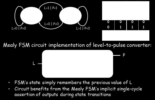
68 While Loops A increasing sequence of values on an output reg [3:0] i, output; i = 0; while (i <= 15) begin output = i; #10 i = i + 1; end 68
69 Blocking vs. Non Blocking Assignments Verilog has two types of procedural assignments Fundamental problem: In a synchronous system, all flip-flops sample simultaneously In Verilog, clk) blocks run in some undefined sequence 69
70 A Flawed Shift Register This doesn t work as you expect: reg d1, d2, d3, d4; clk) d2 = d1; clk) d3 = d2; clk) d4 = d3; These run in some order, but you don t know which 70
71 Non-blocking Assignments This version does work: Nonblocking rule: RHS evaluated when assignment runs reg d1, d2, d3, d4; clk) d2 <= d1; clk) d3 <= d2; clk) d4 <= d3; LHS updated only after all events for the current instant have run. It runs after a Delta time 71
72 Nonblocking Can Behave Oddly A sequence of nonblocking assignments don t communicate a = 1; b = a; c = b; Blocking assignment: a = b = c = 1 a <= 1; b <= a; c <= b; Nonblocking assignment after δ time: a = 1 b = old value of a c = old value of b 72
73 Nonblocking Looks Like Latches RHS of nonblocking taken from latches RHS of blocking taken from wires a = 1; b = a; c = b; 1 a b c a <= 1; b <= a; c <= b; 1 a b c 73
74 Finite State Machines and Verilog 74
75 Finite State Machines Finite State Machines (FSMs) are a useful abstraction for sequential circuits with centralized states of operation At each clock edge, combinational logic computes outputs and next state as a function of inputs and present state inputs + present state Combinational Logic outputs + next state n n CLK Q D Registers 75
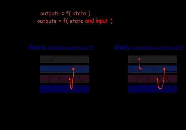
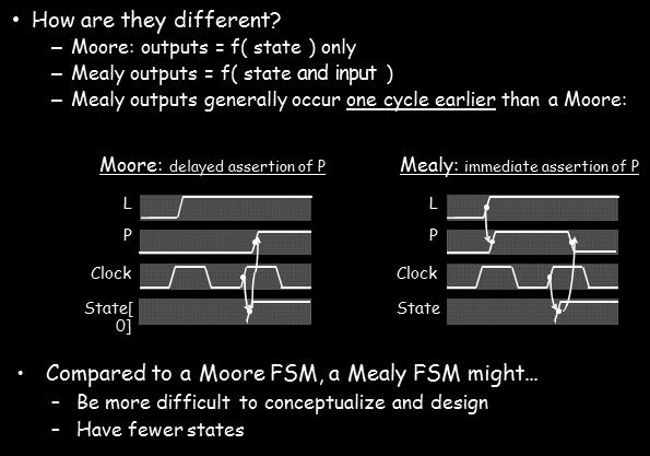
76 Two types of Finite State Machines Moore and Mealy FSMs : different output generation Moore FSM: inputs x 0...x n Comb. Logic next state S' CLK D Q Registers n Comb. Logic Outputs y k = f k (S) present state S Mealy FSM: inputs x 0...x n Comb. Logic next state S' CLK D Q Registers n Comb. Logic Outputs y k = f k (S, x 0...x n ) present state S 76

77 Design Example: Level-to-Pulse A level-to-pulse converter produces a single- cycle pulse each time its input goes high. It s a synchronous rising-edge detector. Sample uses: Buttons and switches pressed by humans for arbitrary periods of time Single-cycle enable signals for counters Whenever input L goes from low to high... CLK L Level to Pulse P Converter...output P produces a single pulse, one clock period wide. 77
 L Level to P Pulse FSM Pulse (P) CLK")
78 Step 1: State Transition Diagram Level (L) L Level to P Pulse FSM Pulse (P) CLK 78

79 Step 2: Logic Derivation + S 0 = L 79

80 Moore Level-to-Pulse Converter 80

81 Design of a Mealy Level-to-Pulse 81

82 Design of a Mealy Level-to-Pulse 82
83 Moore/Mealy Trade-Offs


84 Second FSM Example 84


85 Step 1A: Block Diagram 85

86 Step 1B: State transition diagram
87 Step 2. Verilog Implementation of the FSM module lock(input clk, reset_in, b0, b1, output out); wire reset; parameter S_RESET = 0; parameter S_0= 1; // state assignments parameter S_01 = 2; parameter S_010 = 3; parameter S_0101 = 4; parameter S_01011 = 5; begin // First always computes next state case (state) S_RESET: next_state = b0? S_0 : b1? S_RESET : state; S_0: next_state = b0? S_0 : b1? S_01 : state; S_01: next_state = b0? S_010 : b1? S_RESET : state; S_010: next_state = b0? S_0 : b1? S_0101 : state; S_0101: next_state = b0? S_010 : b1? S_01011 : state; S_01011: next_state = b0? S_0 : b1? S_RESET : state; default: next_state = S_RESET; endcase end // always 87
88 Step 2. Verilog Implementation of the FSM clk) if (reset == 1 b1) state <= S_RESET; else state <=next_state; // Second always computes next state assign out = (state = S_01011); endmodule 88
89 Modeling FSMs Behaviorally There are many ways to do it: 1. Define the next-state logic combinationally and define the state-holding latches explicitly 2. Define the behavior in a single clk) block 89
90 FSM with Combinational Logic module FSM(output reg o, input a, input b, input reset); reg [1:0] state, nextstate; b, state) case (state) 2 b00: begin nextstate = a? 2 b00 : 2 b01; o = a & b; end 2 b01: begin nextstate = 2 b00; o = 0; end endcase Output o is declared a reg because it is assigned procedurally, not because it holds state Combinational block must be sensitive to any change on any of its inputs (Implies state-holding elements otherwise) This is a Mealy FSM: output is sampled every time state or inputs change 90
91 FSM with Combinational Logic module FSM(o, a, b, reset); Latch implied by sensitivity to the clock or reset only clk, reset) if (reset) state <= 2 b00; else state <= nextstate; 91
92 Writing Testbenches module test; reg a, b, sel; Inputs to device under test Device under test (DUT) mux m(y, a, b, sel); initial begin $monitor($time,, a = %b, b=%b, sel=%b, y=%b, a, b, sel, y); a = 0; b= 0; sel = 0; #10 a = 1; #10 sel = 1; #10 b = 1; end endmodule $monitor is a built-in event driven printf Stimulus generated by sequence of assignments and delays 92
93 Writing Testbenches module first_counter_tb(); // Declare inputs as regs and outputs as wires reg clock, reset, enable; wire [3:0] counter_out; //Initialize all variables initial begin $display ("time\t clk reset enable counter"); $monitor ("%g\t %b %b %b %b", $time, clock, reset, enable, counter_out); clock = 1; // initial value of clock reset = 0; // initial value of reset enable = 0; // initial value of enable #5 reset = 1; // Assert the reset #10 reset = 0; // De-assert the reset #10 enable = 1; // Assert enable #100 enable = 0; // De-assert enable #5 $finish; // Terminate simulation end // Clock generator always begin #5 clock = ~clock; // Toggle clock every 5 ticks end // Connect DUT to test bench first_counter U_counter ( clock, reset, enable, counter_out ); end module 93
94 Simulating Verilog 94
95 Simulation Behavior Scheduled using an event queue Non-preemptive, no priorities A process must explicitly request a context switch Events at a particular time unordered Scheduler runs each event at the current time, possibly scheduling more as a result 95
96 Two Types of Events Evaluation events compute functions of inputs Update events change outputs Split necessary for delays, nonblocking assignments, etc. Update event writes new value of a and schedules any evaluation events that are sensitive to a change on a signal a <= b + c Evaluation event reads values of b and c, adds them, and schedules an update event 96
97 Simulation Behavior Concurrent processes (initial, always) run until they stop at one of the following #42 Schedule process to resume 42 time units from now wait(cf & of) Resume when expression cf & of becomes or b or y) Resume when a, b, or y clk) Resume when clk changes from 0 to 1 97
98 Simulation Behavior Infinite loops are possible and the simulator does not check for them This runs forever: no context switch allowed, so ready can never change while (~ready) count = count + 1; Instead, use wait(ready); 98
99 Simulation Behavior Race conditions abound in Verilog These can execute in either order: final value of a undefined: clk) a = 0; clk) a = 1; 99
100 Verilog and Logic Synthesis 100
101 Logic Synthesis Verilog is used in two ways Model for discrete-event simulation Specification for a logic synthesis system Logic synthesis converts a subset of Verilog language into an efficient netlist One of the major breakthroughs in designing logic chips in the last 20 years Most chips are designed using at least some logic synthesis 101
102 Logic Synthesis Tools Mostly commercial tools Very difficult, complicated programs to write well Limited market Commercial products in $10k - $100k price range Major vendors Synopsys Design Compiler, FPGA Express Cadence BuildGates Synplicity (FPGAs) Exemplar (FPGAs) Academic tools SIS (UC Berkeley) 102
103 Logic Synthesis Takes place in two stages: Translation of Verilog (or VHDL) source to a netlist Register inference Optimization of the resulting netlist to improve speed and area 103
104 Logic Optimization Netlist optimization the critical enabling technology Takes a slow or large netlist and transforms it into one that implements the same function more cheaply Typical operations Constant propagation Common subexpression elimination Function factoring Time-consuming operation Can take hours for large chips 104
105 Translating Verilog into Gates Parts of the language easy to translate Structural descriptions with primitives Already a netlist Continuous assignment Expressions turn into little datapaths Behavioral statements the bigger challenge 105
106 What Can Be Translated Structural definitions Everything Behavioral blocks Depends on sensitivity list Only when they have reasonable interpretation as combinational logic, edge, or level-sensitive latches Blocks sensitive to both edges of the clock, changes on unrelated signals, etc. cannot be synthesized User-defined primitives Primitives defined with truth tables Some sequential UDPs can t be translated (not latches or flip-flops) 106
107 What Isn t Translated Initial blocks Used to set up initial state or describe finite testbench stimuli Don t have obvious hardware component Delays May be in the Verilog source, but are ignored by synthesizer A variety of other obscure language features In general, things heavily dependent on discrete-event simulation semantics Certain disable statements 107
108 Register Inference The main trick reg does not always equal latch Rule: Combinational if outputs always depend exclusively on sensitivity list Sequential if outputs may also depend on previous values 108
109 Register Inference Combinational: reg y; or b or sel) if (sel) y = a; else y = b; Sensitive to changes on all of the variables it reads Y is always assigned Sequential: reg q; or clk) if (clk) q = d; q only assigned when clk is 1 109
110 Register Inference A common mistake is not completely specifying a case statement This implies a latch: or b) case ({a, b}) 2 b00 : f = 0; 2 b01 : f = 1; 2 b10 : f = 1; endcase f is not assigned when {a,b} = 2b
111 Register Inference The solution is to always have a default case or b) case ({a, b}) 2 b00: f = 0; 2 b01: f = 1; 2 b10: f = 1; default: f = 0; endcase f is always assigned 111
112 Inferring Latches with Reset Latches and Flip-flops often have reset inputs Can be synchronous or asynchronous Asynchronous positive reset: clk or posedge reset) if (reset) q <= 0; else q <= d; 112
113 Inferring Latches with Reset Synchronous positive reset: clk) if (reset) q <= 0; else q <= d; 113
114 Simulation-synthesis Mismatches Many possible sources of conflict Synthesis ignores delays (e.g., #10), but simulation behavior can be affected by them Simulator models X explicitly, synthesis doesn t Behaviors resulting from shared-variable-like behavior of regs is not synthesized clk) a = 1; New value of a may be seen by clk) statements in simulation, never in synthesis 114
The Verilog Language COMS W Prof. Stephen A. Edwards Fall 2002 Columbia University Department of Computer Science
 The Verilog Language COMS W4995-02 Prof. Stephen A. Edwards Fall 2002 Columbia University Department of Computer Science The Verilog Language Originally a modeling language for a very efficient event-driven
Synthesizable Verilog
 Synthesizable Verilog Courtesy of Dr. Edwards@Columbia, and Dr. Franzon@NCSU http://csce.uark.edu +1 (479) 575-6043 yrpeng@uark.edu Design Methodology Structure and Function (Behavior) of a Design HDL
Introduction To HDL. Verilog HDL. Debdeep Mukhopadhyay Dept of CSE, IIT Madras 1
 Introduction To HDL Verilog HDL Debdeep Mukhopadhyay debdeep@cse.iitm.ernet.in Dept of CSE, IIT Madras 1 How it started! Gateway Design Automation Cadence purchased Gateway in 1989. Verilog was placed
Speaker: Kayting Adviser: Prof. An-Yeu Wu Date: 2009/11/23
 98-1 Under-Graduate Project Synthesis of Combinational Logic Speaker: Kayting Adviser: Prof. An-Yeu Wu Date: 2009/11/23 What is synthesis? Outline Behavior Description for Synthesis Write Efficient HDL
ECE 2300 Digital Logic & Computer Organization. More Sequential Logic Verilog
 ECE 2300 Digital Logic & Computer Organization Spring 2018 More Sequential Logic Verilog Lecture 7: 1 Announcements HW3 will be posted tonight Prelim 1 Thursday March 1, in class Coverage: Lectures 1~7
Verilog. What is Verilog? VHDL vs. Verilog. Hardware description language: Two major languages. Many EDA tools support HDL-based design
 Verilog What is Verilog? Hardware description language: Are used to describe digital system in text form Used for modeling, simulation, design Two major languages Verilog (IEEE 1364), latest version is
FPGA Design Challenge :Techkriti 14 Digital Design using Verilog Part 1
 FPGA Design Challenge :Techkriti 14 Digital Design using Verilog Part 1 Anurag Dwivedi Digital Design : Bottom Up Approach Basic Block - Gates Digital Design : Bottom Up Approach Gates -> Flip Flops Digital
Digital Design with FPGAs. By Neeraj Kulkarni
 Digital Design with FPGAs By Neeraj Kulkarni Some Basic Electronics Basic Elements: Gates: And, Or, Nor, Nand, Xor.. Memory elements: Flip Flops, Registers.. Techniques to design a circuit using basic
Digital Design with SystemVerilog
 Digital Design with SystemVerilog Prof. Stephen A. Edwards Columbia University Spring 25 Synchronous Digital Design Combinational Logic Sequential Logic Summary of Modeling Styles Testbenches Why HDLs?
Online Verilog Resources
 EECS 427 Discussion 6: Verilog HDL Reading: Many references EECS 427 F08 Discussion 6 1 Online Verilog Resources ASICs the book, Ch. 11: http://www.ge.infn.it/~pratolo/verilog/verilogtutorial.pdf it/ pratolo/verilog/verilogtutorial
Lecture 32: SystemVerilog
 Lecture 32: SystemVerilog Outline SystemVerilog module adder(input logic [31:0] a, input logic [31:0] b, output logic [31:0] y); assign y = a + b; Note that the inputs and outputs are 32-bit busses. 17:
101-1 Under-Graduate Project Digital IC Design Flow
 101-1 Under-Graduate Project Digital IC Design Flow Speaker: Ming-Chun Hsiao Adviser: Prof. An-Yeu Wu Date: 2012/9/25 ACCESS IC LAB Outline Introduction to Integrated Circuit IC Design Flow Verilog HDL
Spiral 1 / Unit 4 Verilog HDL. Digital Circuit Design Steps. Digital Circuit Design OVERVIEW. Mark Redekopp. Description. Verification.
 1-4.1 1-4.2 Spiral 1 / Unit 4 Verilog HDL Mark Redekopp OVERVIEW 1-4.3 1-4.4 Digital Circuit Design Steps Digital Circuit Design Description Design and computer-entry of circuit Verification Input Stimulus
N-input EX-NOR gate. N-output inverter. N-input NOR gate
 Hardware Description Language HDL Introduction HDL is a hardware description language used to design and document electronic systems. HDL allows designers to design at various levels of abstraction. It
Lecture #2: Verilog HDL
 Lecture #2: Verilog HDL Paul Hartke Phartke@stanford.edu Stanford EE183 April 8, 2002 EE183 Design Process Understand problem and generate block diagram of solution Code block diagram in verilog HDL Synthesize
Verilog for Synthesis Ing. Pullini Antonio
 Verilog for Synthesis Ing. Pullini Antonio antonio.pullini@epfl.ch Outline Introduction to Verilog HDL Describing combinational logic Inference of basic combinational blocks Describing sequential circuits
Chapter 2 Using Hardware Description Language Verilog. Overview
 Chapter 2 Using Hardware Description Language Verilog CSE4210 Winter 2012 Mokhtar Aboelaze based on slides by Dr. Shoab A. Khan Overview Algorithm development isa usually done in MATLAB, C, or C++ Code
Introduction To HDL. Verilog HDL. Debdeep Mukhopadhyay How it started!
 Introduction To HDL Verilog HDL Debdeep Mukhopadhyay debdeep@cse.iitm.ernet.in Dept of CSE, IIT Madras 1 How it started! Gateway Design Automation Cadence purchased Gateway in 1989. Verilog was placed
Design Using Verilog
 EGC220 Design Using Verilog Baback Izadi Division of Engineering Programs bai@engr.newpaltz.edu Basic Verilog Lexical Convention Lexical convention are close to C++. Comment // to the of the line. /* to
CSE140L: Components and Design Techniques for Digital Systems Lab. Verilog HDL. Instructor: Mohsen Imani UC San Diego. Source: Eric Crabill, Xilinx
 CSE140L: Components and Design Techniques for Digital Systems Lab Verilog HDL Instructor: Mohsen Imani UC San Diego Source: Eric Crabill, Xilinx 1 Hardware description languages Used to describe & model
Synthesis of Combinational and Sequential Circuits with Verilog
 Synthesis of Combinational and Sequential Circuits with Verilog What is Verilog? Hardware description language: Are used to describe digital system in text form Used for modeling, simulation, design Two
Lecture 15: System Modeling and Verilog
 Lecture 15: System Modeling and Verilog Slides courtesy of Deming Chen Intro. VLSI System Design Outline Outline Modeling Digital Systems Introduction to Verilog HDL Use of Verilog HDL in Synthesis Reading
EECS 427 Lecture 14: Verilog HDL Reading: Many handouts/references. EECS 427 W07 Lecture 14 1
 EECS 427 Lecture 14: Verilog HDL Reading: Many handouts/references EECS 427 W07 Lecture 14 1 Online Verilog Resources ASICs the book, Ch. 11: http://www.ge.infn.it/~pratolo/verilog/verilogtutorial.pdf
This Lecture. Some components (useful for the homework) Verilog HDL (will continue next lecture)
 Verilog HDL (will continue next lecture)") Last Lecture The basic component of a digital circuit is the MOS transistor Transistor have instrinsic resistance and capacitance, so voltage values in the circuit take some time to change ( delay ) There
Last Lecture The basic component of a digital circuit is the MOS transistor Transistor have instrinsic resistance and capacitance, so voltage values in the circuit take some time to change ( delay ) There
Computer Aided Design Basic Syntax Gate Level Modeling Behavioral Modeling. Verilog
 Verilog Radek Pelánek and Šimon Řeřucha Contents 1 Computer Aided Design 2 Basic Syntax 3 Gate Level Modeling 4 Behavioral Modeling Computer Aided Design Hardware Description Languages (HDL) Verilog C
CSE140L: Components and Design
 CSE140L: Components and Design Techniques for Digital Systems Lab Tajana Simunic Rosing Source: Vahid, Katz, Culler 1 Grade distribution: 70% Labs 35% Lab 4 30% Lab 3 20% Lab 2 15% Lab 1 30% Final exam
Verilog HDL Introduction
 EEE3050 Theory on Computer Architectures (Spring 2017) Prof. Jinkyu Jeong Verilog HDL Introduction 2017.05.14 TA 이규선 (GYUSUN LEE) / 안민우 (MINWOO AHN) Modules The Module Concept Basic design unit Modules
What is Verilog HDL? Lecture 1: Verilog HDL Introduction. Basic Design Methodology. What is VHDL? Requirements
 What is Verilog HDL? Lecture 1: Verilog HDL Introduction Verilog Hardware Description Language(HDL)? A high-level computer language can model, represent and simulate digital design Hardware concurrency
CSE140L: Components and Design Techniques for Digital Systems Lab
 CSE140L: Components and Design Techniques for Digital Systems Lab Tajana Simunic Rosing Source: Vahid, Katz, Culler 1 Announcements & Outline Lab 4 due; demo signup times listed on the cse140l site Check
Verilog Design Principles
 16 h7fex // 16-bit value, low order 4 bits unknown 8 bxx001100 // 8-bit value, most significant 2 bits unknown. 8 hzz // 8-bit value, all bits high impedance. Verilog Design Principles ECGR2181 Extra Notes
FPGA: FIELD PROGRAMMABLE GATE ARRAY Verilog: a hardware description language. Reference: [1]
![FPGA: FIELD PROGRAMMABLE GATE ARRAY Verilog: a hardware description language. Reference: [1]](/thumbs/80/81661285.jpg "FPGA: FIELD PROGRAMMABLE GATE ARRAY Verilog: a hardware description language. Reference: [1]") FPGA: FIELD PROGRAMMABLE GATE ARRAY Verilog: a hardware description language Reference: [] FIELD PROGRAMMABLE GATE ARRAY FPGA is a hardware logic device that is programmable Logic functions may be programmed
FPGA: FIELD PROGRAMMABLE GATE ARRAY Verilog: a hardware description language Reference: [] FIELD PROGRAMMABLE GATE ARRAY FPGA is a hardware logic device that is programmable Logic functions may be programmed
IT T35 Digital system desigm y - ii /s - iii
 UNIT - V Introduction to Verilog Hardware Description Language Introduction HDL for combinational circuits Sequential circuits Registers and counters HDL description for binary multiplier. 5.1 INTRODUCTION
A Brief Introduction to Verilog Hardware Definition Language (HDL)
") www.realdigital.org A Brief Introduction to Verilog Hardware Definition Language (HDL) Forward Verilog is a Hardware Description language (HDL) that is used to define the structure and/or behavior of digital
www.realdigital.org A Brief Introduction to Verilog Hardware Definition Language (HDL) Forward Verilog is a Hardware Description language (HDL) that is used to define the structure and/or behavior of digital
Combinational Logic II
 Combinational Logic II Ranga Rodrigo July 26, 2009 1 Binary Adder-Subtractor Digital computers perform variety of information processing tasks. Among the functions encountered are the various arithmetic
ECE 353 Lab 4. Verilog Review. Professor Daniel Holcomb With material by Professor Moritz and Kundu UMass Amherst Fall 2016
 ECE 353 Lab 4 Verilog Review Professor Daniel Holcomb With material by Professor Moritz and Kundu UMass Amherst Fall 2016 Recall What You Will Do Design and implement a serial MIDI receiver Hardware in
Why Should I Learn This Language? VLSI HDL. Verilog-2
 Verilog Why Should I Learn This Language? VLSI HDL Verilog-2 Different Levels of Abstraction Algorithmic the function of the system RTL the data flow the control signals the storage element and clock Gate
Introduction to Digital Design with Verilog HDL
 Introduction to Digital Design with Verilog HDL Modeling Styles 1 Levels of Abstraction n Behavioral The highest level of abstraction provided by Verilog HDL. A module is implemented in terms of the desired
Contents. Appendix D Verilog Summary Page 1 of 16
 Appix D Verilog Summary Page 1 of 16 Contents Appix D Verilog Summary... 2 D.1 Basic Language Elements... 2 D.1.1 Keywords... 2 D.1.2 Comments... 2 D.1.3 Identifiers... 2 D.1.4 Numbers and Strings... 3
EEL 4783: HDL in Digital System Design
 EEL 4783: HDL in Digital System Design Lecture 15: Logic Synthesis with Verilog Prof. Mingjie Lin 1 Verilog Synthesis Synthesis vs. Compilation Descriptions mapped to hardware Verilog design patterns for
Synthesis vs. Compilation Descriptions mapped to hardware Verilog design patterns for best synthesis. Spring 2007 Lec #8 -- HW Synthesis 1
 Verilog Synthesis Synthesis vs. Compilation Descriptions mapped to hardware Verilog design patterns for best synthesis Spring 2007 Lec #8 -- HW Synthesis 1 Logic Synthesis Verilog and VHDL started out
A Verilog Primer. An Overview of Verilog for Digital Design and Simulation
 A Verilog Primer An Overview of Verilog for Digital Design and Simulation John Wright Vighnesh Iyer Department of Electrical Engineering and Computer Sciences College of Engineering, University of California,
Introduction to Verilog/System Verilog
 NTUEE DCLAB Feb. 27, 2018 Introduction to Verilog/System Verilog Presenter: Yao-Pin Wang 王耀斌 Advisor: Prof. Chia-Hsiang Yang 楊家驤 Dept. of Electrical Engineering, NTU National Taiwan University What is
VLSI Design 13. Introduction to Verilog
 Last module: Sequential circuit design Design styles This module Synthesis Brief introduction to Verilog Synthesis in the Design Flow Designer Tasks Tools Architect Logic Designer Circuit Designer Define
Verilog. Like VHDL, Verilog HDL is like a programming language but:
 Verilog Verilog Like VHDL, Verilog HDL is like a programming language but: Statements can execute simultaneously unlike programming e.g. nand(y1,a1,b1); nand(y2,a2,b2); or (out,y1,y2); a1 b1 all statements
Chapter 4 :: Topics. Introduction. SystemVerilog. Hardware description language (HDL): allows designer to specify logic function only.
: allows designer to specify logic function only.") Chapter 4 :: Hardware Description Languages Digital Design and Computer Architecture David Money Harris and Sarah L. Harris Chapter 4 :: Topics Introduction Combinational Logic Structural Modeling Sequential
Chapter 4 :: Hardware Description Languages Digital Design and Computer Architecture David Money Harris and Sarah L. Harris Chapter 4 :: Topics Introduction Combinational Logic Structural Modeling Sequential
Under-Graduate Project Logic Design with Behavioral Models
 97-1 1 Under-Graduate Project Logic Design with Behavioral Models Speaker: 吳佳謙 Adviser: Prof. An-Yeu Wu Date: 2008/10/20 ACCESS IC LAB Operation Assignment Outline Blocking and non-blocking Appendix pp.
Introduction. Why Use HDL? Simulation output. Explanation
 Introduction Verilog HDL is a Hardware Description Language (HDL) HDL is a language used to describe a digital system, for example, a computer or a component of a computer. Most popular HDLs are VHDL and
a, b sum module add32 sum vector bus sum[31:0] sum[0] sum[31]. sum[7:0] sum sum overflow module add32_carry assign
![a, b sum module add32 sum vector bus sum[31:0] sum[0] sum[31]. sum[7:0] sum sum overflow module add32_carry assign](/thumbs/91/106466219.jpg "a, b sum module add32 sum vector bus sum[31:0] sum[0] sum[31]. sum[7:0] sum sum overflow module add32_carry assign") I hope you have completed Part 1 of the Experiment. This lecture leads you to Part 2 of the experiment and hopefully helps you with your progress to Part 2. It covers a number of topics: 1. How do we specify
I hope you have completed Part 1 of the Experiment. This lecture leads you to Part 2 of the experiment and hopefully helps you with your progress to Part 2. It covers a number of topics: 1. How do we specify
14:332:231 DIGITAL LOGIC DESIGN. Hardware Description Languages
 14:332:231 DIGITAL LOGIC DESIGN Ivan Marsic, Rutgers University Electrical & Computer Engineering Fall 2013 Lecture #22: Introduction to Verilog Hardware Description Languages Basic idea: Language constructs
ECE 353 Lab 4. Verilog Review. Professor Daniel Holcomb UMass Amherst Fall 2017
 ECE 353 Lab 4 Verilog Review Professor Daniel Holcomb UMass Amherst Fall 2017 What You Will Do In Lab 4 Design and implement a serial MIDI receiver Hardware in an Altera Complex Programmable Logic Device
Verilog introduction. Embedded and Ambient Systems Lab
 Verilog introduction Embedded and Ambient Systems Lab Purpose of HDL languages Modeling hardware behavior Large part of these languages can only be used for simulation, not for hardware generation (synthesis)
Introduction to Verilog design. Design flow (from the book)
") Introduction to Verilog design Lecture 2 ECE 156A 1 Design flow (from the book) ECE 156A 2 1 Hierarchical Design Chip Modules Cells Primitives A chip contain many modules A module may contain other modules
Introduction to Verilog design Lecture 2 ECE 156A 1 Design flow (from the book) ECE 156A 2 1 Hierarchical Design Chip Modules Cells Primitives A chip contain many modules A module may contain other modules
Lecture 12 VHDL Synthesis
 CPE 487: Digital System Design Spring 2018 Lecture 12 VHDL Synthesis Bryan Ackland Department of Electrical and Computer Engineering Stevens Institute of Technology Hoboken, NJ 07030 1 What is Synthesis?
Verilog Tutorial (Structure, Test)
") Digital Circuit Design and Language Verilog Tutorial (Structure, Test) Chang, Ik Joon Kyunghee University Hierarchical Design Top-down Design Methodology Bottom-up Design Methodology Module START Example)
Digital Circuit Design and Language Verilog Tutorial (Structure, Test) Chang, Ik Joon Kyunghee University Hierarchical Design Top-down Design Methodology Bottom-up Design Methodology Module START Example)
Verilog Coding Guideline
 Verilog Coding Guideline Digital Circuit Lab TA: Po-Chen Wu Outline Introduction to Verilog HDL Verilog Syntax Combinational and Sequential Logics Module Hierarchy Write Your Design Finite State Machine
Register Transfer Level in Verilog: Part I
 Source: M. Morris Mano and Michael D. Ciletti, Digital Design, 4rd Edition, 2007, Prentice Hall. Register Transfer Level in Verilog: Part I Lan-Da Van ( 范倫達 ), Ph. D. Department of Computer Science National
Introduction to Verilog design. Design flow (from the book) Hierarchical Design. Lecture 2
 Hierarchical Design. Lecture 2") Introduction to Verilog design Lecture 2 ECE 156A 1 Design flow (from the book) ECE 156A 2 Hierarchical Design Chip Modules Cells Primitives A chip contain many modules A module may contain other modules
Introduction to Verilog design Lecture 2 ECE 156A 1 Design flow (from the book) ECE 156A 2 Hierarchical Design Chip Modules Cells Primitives A chip contain many modules A module may contain other modules
EECS150 - Digital Design Lecture 10 Logic Synthesis
 EECS150 - Digital Design Lecture 10 Logic Synthesis September 26, 2002 John Wawrzynek Fall 2002 EECS150 Lec10-synthesis Page 1 Logic Synthesis Verilog and VHDL stated out as simulation languages, but quickly
EN2911X: Reconfigurable Computing Topic 02: Hardware Definition Languages
 EN2911X: Reconfigurable Computing Topic 02: Hardware Definition Languages Professor Sherief Reda http://scale.engin.brown.edu School of Engineering Brown University Spring 2014 1 Introduction to Verilog
Lecture 3: Modeling in VHDL. EE 3610 Digital Systems
 EE 3610: Digital Systems 1 Lecture 3: Modeling in VHDL VHDL: Overview 2 VHDL VHSIC Hardware Description Language VHSIC=Very High Speed Integrated Circuit Programming language for modelling of hardware
Outline. EECS Components and Design Techniques for Digital Systems. Lec 11 Putting it all together Where are we now?
 Outline EECS 5 - Components and Design Techniques for Digital Systems Lec Putting it all together -5-4 David Culler Electrical Engineering and Computer Sciences University of California Berkeley Top-to-bottom
Logic Synthesis. EECS150 - Digital Design Lecture 6 - Synthesis
 Logic Synthesis Verilog and VHDL started out as simulation languages, but quickly people wrote programs to automatically convert Verilog code into low-level circuit descriptions (netlists). EECS150 - Digital
Introduction to Verilog HDL. Verilog 1
 Introduction to HDL Hardware Description Language (HDL) High-Level Programming Language Special constructs to model microelectronic circuits Describe the operation of a circuit at various levels of abstraction
Microcomputers. Outline. Number Systems and Digital Logic Review
 Microcomputers Number Systems and Digital Logic Review Lecture 1-1 Outline Number systems and formats Common number systems Base Conversion Integer representation Signed integer representation Binary coded
HDLs and SystemVerilog. Digital Computer Design
 HDLs and SystemVerilog Digital Computer Design Logic Arrays Gates can be organized into regular arrays. If the connections are made programmable, these logic arrays can be configured to perform any function
Verilog Tutorial. Introduction. T. A.: Hsueh-Yi Lin. 2008/3/12 VLSI Digital Signal Processing 2
 Verilog Tutorial T. A.: Hsueh-Yi Lin Introduction 2008/3/12 VLSI Digital Signal Processing 2 Verilog: A common language for industry HDL is a common way for hardware design Verilog VHDL Verilog is widely
CSE241 VLSI Digital Circuits Winter Recitation 1: RTL Coding in Verilog
 CSE241 VLSI Digital Circuits Winter 2003 Recitation 1: RTL Coding in Verilog CSE241 R1 Verilog.1 Kahng & Cichy, UCSD 2003 Topic Outline Introduction Verilog Background Connections Modules Procedures Structural
Speaker: Shao-Wei Feng Adviser: Prof. An-Yeu Wu Date: 2010/09/28
 99-1 Under-Graduate Project Verilog Simulation & Debugging Tools Speaker: Shao-Wei Feng Adviser: Prof. An-Yeu Wu Date: 2010/09/28 ACCESS IC LAB Outline Basic Concept of Verilog HDL Gate Level Modeling
Hardware description languages
 Specifying digital circuits Schematics (what we ve done so far) Structural description Describe circuit as interconnected elements Build complex circuits using hierarchy Large circuits are unreadable Hardware
Verilog 1 - Fundamentals
 Verilog 1 - Fundamentals FA FA FA FA module adder( input [3:0] A, B, output cout, output [3:0] S ); wire c0, c1, c2; FA fa0( A[0], B[0], 1 b0, c0, S[0] ); FA fa1( A[1], B[1], c0, c1, S[1] ); FA fa2( A[2],
Schematic design. Gate level design. 0 EDA (Electronic Design Assistance) 0 Classical design. 0 Computer based language
 0 Classical design. 0 Computer based language") 1 / 15 2014/11/20 0 EDA (Electronic Design Assistance) 0 Computer based language 0 HDL (Hardware Description Language) 0 Verilog HDL 0 Created by Gateway Design Automation Corp. in 1983 First modern hardware
1 / 15 2014/11/20 0 EDA (Electronic Design Assistance) 0 Computer based language 0 HDL (Hardware Description Language) 0 Verilog HDL 0 Created by Gateway Design Automation Corp. in 1983 First modern hardware
EECS150 - Digital Design Lecture 10 Logic Synthesis
 EECS150 - Digital Design Lecture 10 Logic Synthesis February 13, 2003 John Wawrzynek Spring 2003 EECS150 Lec8-synthesis Page 1 Logic Synthesis Verilog and VHDL started out as simulation languages, but
Hardware Design Environments. Dr. Mahdi Abbasi Computer Engineering Department Bu-Ali Sina University
 Hardware Design Environments Dr. Mahdi Abbasi Computer Engineering Department Bu-Ali Sina University Outline Welcome to COE 405 Digital System Design Design Domains and Levels of Abstractions Synthesis
Chap 6 Introduction to HDL (d)
") Design with Verilog Chap 6 Introduction to HDL (d) Credit to: MD Rizal Othman Faculty of Electrical & Electronics Engineering Universiti Malaysia Pahang Ext: 6036 VERILOG HDL Basic Unit A module Module
Design with Verilog Chap 6 Introduction to HDL (d) Credit to: MD Rizal Othman Faculty of Electrical & Electronics Engineering Universiti Malaysia Pahang Ext: 6036 VERILOG HDL Basic Unit A module Module
CS6710 Tool Suite. Verilog is the Key Tool
 CS6710 Tool Suite Verilog-XL Behavioral Verilog Your Library Cadence SOC Encounter Synopsys Synthesis Structural Verilog Circuit Layout CSI Verilog-XL AutoRouter Cadence Virtuoso Layout LVS Layout-XL Cadence
VHDL: RTL Synthesis Basics. 1 of 59
 VHDL: RTL Synthesis Basics 1 of 59 Goals To learn the basics of RTL synthesis. To be able to synthesize a digital system, given its VHDL model. To be able to relate VHDL code to its synthesized output.
Verilog Module 1 Introduction and Combinational Logic
 Verilog Module 1 Introduction and Combinational Logic Jim Duckworth ECE Department, WPI 1 Module 1 Verilog background 1983: Gateway Design Automation released Verilog HDL Verilog and simulator 1985: Verilog
The Verilog Hardware Description Language
 The Verilog Hardware Description Language Professor Don Thomas Carnegie Mellon University (CMU) thomas@ece.cmu.edu http://www.ece.cmu.edu/~thomas n This is not one cohesive presentation on Verilog. The
Verilog for High Performance
 Verilog for High Performance Course Description This course provides all necessary theoretical and practical know-how to write synthesizable HDL code through Verilog standard language. The course goes
Verilog Overview. The Verilog Hardware Description Language. Simulation of Digital Systems. Simulation of Digital Systems. Don Thomas, 1998, Page 1
 The Verilog Hardware Description Language These slides were created by Prof. Dan Thomas at Carnegie Mellon University, and are adapted here with permission. The Verilog Hardware Description Language, Fourth
Verilog Fundamentals. Shubham Singh. Junior Undergrad. Electrical Engineering
 Verilog Fundamentals Shubham Singh Junior Undergrad. Electrical Engineering VERILOG FUNDAMENTALS HDLs HISTORY HOW FPGA & VERILOG ARE RELATED CODING IN VERILOG HDLs HISTORY HDL HARDWARE DESCRIPTION LANGUAGE
Hardware Description Language VHDL (1) Introduction
 Introduction") Hardware Description Language VHDL (1) Introduction Digital Radiation Measurement and Spectroscopy NE/RHP 537 Introduction Hardware description language (HDL) Intended to describe circuits textually, for
Hardware Description Language VHDL (1) Introduction Digital Radiation Measurement and Spectroscopy NE/RHP 537 Introduction Hardware description language (HDL) Intended to describe circuits textually, for
14. Introducton to Verilog
 14. Introducton to Verilog Jacob Abraham Department of Electrical and Computer Engineering The University of Texas at Austin VLSI Design Fall 2017 October 23, 2017 ECE Department, University of Texas at
Programmable Logic Devices Verilog VII CMPE 415
 Synthesis of Combinational Logic In theory, synthesis tools automatically create an optimal gate-level realization of a design from a high level HDL description. In reality, the results depend on the skill
Quick Introduction to SystemVerilog: Sequental Logic
 ! Quick Introduction to SystemVerilog: Sequental Logic Lecture L3 8-545 Advanced Digital Design ECE Department Many elements Don Thomas, 24, used with permission with credit to G. Larson Today Quick synopsis
Verilog Overview. The Verilog Hardware Description Language. Simulation of Digital Systems. Simulation of Digital Systems. Don Thomas, 1998, Page 1
 The Verilog Hardware Description Language These slides were created by Prof. Don Thomas at Carnegie Mellon University, and are adapted here with permission. The Verilog Hardware Description Language, Fifth
Sequential Logic Design
 Sequential Logic Design Design of Digital Circuits 2017 Srdjan Capkun Onur Mutlu (Guest starring: Frank K. Gürkaynak and Aanjhan Ranganathan) http://www.syssec.ethz.ch/education/digitaltechnik_17 Adapted
EECS150 - Digital Design Lecture 5 - Verilog Logic Synthesis
 EECS150 - Digital Design Lecture 5 - Verilog Logic Synthesis Jan 31, 2012 John Wawrzynek Spring 2012 EECS150 - Lec05-verilog_synth Page 1 Outline Quick review of essentials of state elements Finite State
Introduction To Verilog Design. Chun-Hung Chou
 Introduction To Verilog Design Chun-Hung Chou 1 Outline Typical Design Flow Design Method Lexical Convention Data Type Data Assignment Event Control Conditional Description Register Description Synthesizable
In this lecture, we will go beyond the basic Verilog syntax and examine how flipflops and other clocked circuits are specified.
 1 In this lecture, we will go beyond the basic Verilog syntax and examine how flipflops and other clocked circuits are specified. I will also introduce the idea of a testbench as part of a design specification.
Hardware Description Language (HDL)
") Hardware Description Language (HDL) What is the need for Hardware Description Language? Model, Represent, And Simulate Digital Hardware Hardware Concurrency Parallel Activity Flow Semantics for Signal
Hardware Description Language (HDL) What is the need for Hardware Description Language? Model, Represent, And Simulate Digital Hardware Hardware Concurrency Parallel Activity Flow Semantics for Signal
Verilog Overview. The Verilog Hardware Description Language. Simulation of Digital Systems. Simulation of Digital Systems. Don Thomas, 1998, Page 1
 The Verilog Hardware Description Language These slides were created by Prof. Don Thomas at Carnegie Mellon University, and are adapted here with permission. The Verilog Hardware Description Language, Fifth
Topics. Midterm Finish Chapter 7
 Lecture 9 Topics Midterm Finish Chapter 7 ROM (review) Memory device in which permanent binary information is stored. Example: 32 x 8 ROM Five input lines (2 5 = 32) 32 outputs, each representing a memory
Lecture 2: Data Types, Modeling Combinational Logic in Verilog HDL. Variables and Logic Value Set. Data Types. Why use an HDL?
 Why use an HDL? Lecture 2: Data Types, Modeling Combinational Logic in Verilog HDL Increase digital design engineer s productivity (from Dataquest) Behavioral HDL RTL HDL Gates Transistors 2K 10K gates/week
Chapter 3: Dataflow Modeling
 Chapter 3: Dataflow Modeling Prof. Soo-Ik Chae Digital System Designs and Practices Using Verilog HDL and FPGAs @ 2008, John Wiley 3-1 Objectives After completing this chapter, you will be able to: Describe
VHDL. VHDL History. Why VHDL? Introduction to Structured VLSI Design. Very High Speed Integrated Circuit (VHSIC) Hardware Description Language
 Hardware Description Language") VHDL Introduction to Structured VLSI Design VHDL I Very High Speed Integrated Circuit (VHSIC) Hardware Description Language Joachim Rodrigues A Technology Independent, Standard Hardware description Language
VHDL Introduction to Structured VLSI Design VHDL I Very High Speed Integrated Circuit (VHSIC) Hardware Description Language Joachim Rodrigues A Technology Independent, Standard Hardware description Language
Chapter 4. Digital Design and Computer Architecture, 2 nd Edition. David Money Harris and Sarah L. Harris. Chapter 4 <1>
 Chapter 4 Digital Design and Computer Architecture, 2 nd Edition David Money Harris and Sarah L. Harris Chapter 4 Chapter 4 :: Topics Introduction Combinational Logic Structural Modeling Sequential
DIGITAL SYSTEM DESIGN
 DIGITAL SYSTEM DESIGN Prepared By: Engr. Yousaf Hameed Lab Engineer BASIC ELECTRICAL & DIGITAL SYSTEMS LAB DEPARTMENT OF ELECTRICAL ENGINEERING Digital System Design 1 Name: Registration No: Roll No: Semester:
ECE 353 Lab 3 (Verilog Design Approach)
") ECE 353 Lab 3 (Verilog Design Approach) Prof Daniel Holcomb Recall What You Will Do Design and implement a serial MIDI receiver Hardware in an Altera Complex Programmable Logic Device (CPLD) MAX 7000S
ECE 353 Lab 3 (Verilog Design Approach) Prof Daniel Holcomb Recall What You Will Do Design and implement a serial MIDI receiver Hardware in an Altera Complex Programmable Logic Device (CPLD) MAX 7000S
Verilog 1 - Fundamentals
 Verilog 1 - Fundamentals FA FA FA FA module adder( input [3:0] A, B, output cout, output [3:0] S ); wire c0, c1, c2; FA fa0( A[0], B[0], 1 b0, c0, S[0] ); FA fa1( A[1], B[1], c0, c1, S[1] ); FA fa2( A[2],